Fabrication of plastic microchips by hot embossing
Larry J.
Kricka
a,
Paolo
Fortina
b,
Nicholas J.
Panaro
a,
Peter
Wilding
a,
Goretty
Alonso-Amigo
c and
Holger
Becker
c
aDepartments of Pathology and Laboratory Medicine, University of Pennsylvania School of Medicine, Philadelphia, PA 19104, USA
bDepartment of Pediatrics, University of Pennsylvania School of Medicine and The Children′s Hospital of Philadelphia, Philadelphia, PA 19104, USA
cMildendo, Goschwitzer Str 40, Jena, Germany
First published on 21st January 2002
Abstract
Plastic microchips with microchannels (100 µm wide, 40 µm deep) of varying designs have been fabricated in polymethylmethacrylate by a hot embossing process using an electroform tool produced starting with silicon chip masters. Hot-embossed chips were capped with a polymethylmethacrylate top using a proprietary solvent bonding process. Holes were drilled through the top of the chip to allow access to the channels. The chips were tested with fluid and shown to fill easily. The seal between the top of the chip and the hot embossed base was effective, and there was no leakage from the channels when fluid was pumped through the microchannels. The chips were also tested with a semen sample and the plastic chip performed identically to the previous silicon–glass and glass versions of the chip. This microfabrication technique offers a viable and potentially high-volume low cost production method for fabricating transparent microchips for analytical applications.
Introduction
A wide range of microchip devices have been developed, and the majority have been fabricated from either silicon or glass or a combination of silicon or glass.1–3 Silicon chips are not transparent thus limiting their utility in applications that require inspection using conventional transmission microscopy. Glass chips do not have this limitation, but are more difficult to manufacture, particularly the bonding of the two pieces of glass that comprise the chip.4–7 Plastics and other polymeric materials have several advantages as construction materials for microchips. They are amenable to a more varied range of high volume low-cost production techniques, and provide a diverse range of physical properties (e.g., surface properties). Previously, plastic microchips have been fabricated from poly(methylmethacrylate)(PMMA),8–10 polydimethylsiloxane (PDMS),11–13 polycarbonate,14 polyimide,15 and used for a variety of analytical techniques including capillary electrophoresis,16–19 isotachophoresis,8 isoelectric focussing,14 DNA sequencing,20 chromatography,21 and immunoassay.22 Fabrication methods for plastic chips include wire-imprinting,23 hot-embossing,24 molding,25 laser micromachining/abalation,26,27 X-ray lithography,28 and lamination techniques.15 In this study we investigated the production of PMMA versions of sperm chips previously fabricated in silicon29 using the original silicon chips as the masters for making the hot embossing tool. The analytical features in the resulting PMMA chips were a true replica of the features in the original silicon chips and the assembled chip filled easily with fluid and did not leak when the microchannels were filled with fluid or semen.Experimental
Silicon master
A series of silicon sperm chips described previously29 were used to prepare the electroform tool. The basic design of the chips is a pair of 40 µm deep, square troughs (1 × 1 mm and 2 × 2 mm) connected by a microchannel (100 µm wide, 40 µm deep) of varying length and complexity (Fig. 1). The different channel designs varied in length from 8.5 mm to 48.5 mm and had between 4 and 22 right angle turns. The volume of the different microchannels ranged from 37.2 to 280 nL, the two troughs in the silicon at the end of each channel had volumes of 80 and 160 nL, respectively. Three of these structures are etched onto the surface of each chip. Masks for the fabrication process were made by Align-Rite (Santa Clara, CA), the 4 inch silicon wafers (560–590 µm thick) were etched by Micrel Semiconductor (San Jose, CA) and diced into 17 × 14 mm chips by the Alberta Microelectronics Centre (Edmonton, Alberta). | ||
| Fig. 1 Electroform tool (100 ± 1 mm diameter, 2 mm thick) produced from four diced silicon microfabricated chips by an electroplating process. | ||
Electroform tool
Four diced silicon microfabricated chips with positive features defining different channel geometries were used as the masters in the preparation of an electroform tool for plastic replication. The four chips were assembled on a flat substrate using a low viscosity epoxy adhesive. The objective was to maintain the four chips coplanar. Coplanarity is very important for the hot embossing process in order to ensure even replication of all the structures and the enclosure of all channels during the bonding.This assembly of four chips was electroplated using a standard nickel sulfate galvanomic process after sputtering a layer of silver of about 1000 Å. The electroplating process was carried out for several days to form a 4 mm thick stamper. In order to prepare a final tool for hot embossing, the back of the stamper was flattened by a lapping process and machined to form a round Nickel wafer of 100 ± 1 mm in diameter and 2 mm thickness. The resulting tool had a front flatness of about 500 microns and a back flatness of about 50 microns. After a single electroplating process, the tool had accurate negative replicas of the channel structures, defined in the tool as ridges, and was ready to fit into the hot embossing tool holder.
Hot embossing and sealing
Replication of the channel by hot embossing was performed using premolded polymethylmethacrylate (PMMA) wafers on a HEX-02 system from Jenoptik Mikrotechnik GmbH (Jena, Germany). These substrate wafers were prepared using an injection molding process and a commercial Perspex resin from Imperial Chemical Industries (Runcorn, UK). The principles and process of microreplication by hot embossing are described in detailed elsewhere.30 In practice, the replication in PMMA is performed about 20 °C above the glass transition temperature (Tg) of the plastic resin with embossing pressures of about 3 N mm−2.After replication, each plastic wafer had 1 mm holes drilled at the inlet and outlet positions of each channel. This was performed using a CO2 laser.30,31 The laser-drilled holes are defined to provide entry and exit ports to the channel structure and to contain 1–2 µL volumes of liquid sample. Each plastic wafer was sealed with a flat cover (17 × 14 mm) of the same material using a proprietary bonding methodology developed by Jenoptik Mikrotechnik GmbH. After bonding, all the channel structures in the four chips were sealed and ready for dicing by CO2 laser cutting. Thus, drilled holes sealed on one side by the bonded cover plate become wells at each end of a channel.
Profilometer
The quality of the embossed microchannels was checked using a Wyko NT 3300 profilometer (Veeco Metrology Group, Tucson, Arizona).Inspection and testing with fluids
In order to assess the effectiveness of the sealing of the top onto the hot embossed micropart, New Methylene Blue (Sigma, St Louis, MO; 1∶10 in phosphate buffered saline (PBS)) was introduced into the channels using a 10 µL Micropipetman (Rainin L-10, Woburn, MA). Microscopic examination of the chips was performed using a Leica Aristomet microscope (Leica Microsytems, Inc., Bannockburn, IL). Real-time digital images (MPEG1, 320 × 240 pixels) were captured using a Panasonic GP-KR222 CCD camera (Matsuchita Electric Works, Ltd., Osaka, Japan) mounted on the microscope in conjunction with Broadway Pro 5.1 software (Data Translation, Inc., Marlboro, MA) run on an HP Vectra computer (Hewlett Packard, Palo Alto, CA; NT 4.0 operating system). A raw semen sample (0.5-1 µL) was introduced into one end of a channel filled with human tubal fluid medium (Irvine Scientific, CA) containing 0.5% bovine serum albumin (ICN Biomedicals, OH) and the progress of sperm along the channel monitored using the microscope and video capture system.Results and discussion
The embossing process using the electroform tool (Fig. 1) produced accurate replicas of the original microchannel designs (Fig. 2). A comparison of the 3D images of the channel entrance to a reservoir on the electroform tool and on the replicated PMMA micropart produced by hot embossing revealed no major discrepancies. The bonded micropart was tested with an aqueous dye solution to investigate ease of filling of the channels, and to test the effectiveness of the bonding of the PMMA top to the hot embossed micropart. Multiple channels on several chips were tested. All filled easily and no leaks were detected (particularly egress of fluid from the top of the channel into space between possibly unbonded parts of the chip) when the different designs of microchannel were completely filled with fluid and observed for >20 min. One of the chips was also tested using a semen sample. Sperm were observed swimming along the channel. None of the sperm were observed to penetrate under the top of the chip indicating an effective seal between the two parts of the chip at the edge the channel shown to be problematic in previous attempts to fabricate plastic chips.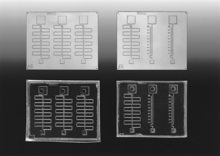 | ||
| Fig. 2 Uncapped 17 × 14 mm silicon sperm microchips (two different designs) (upper) and capped PMMA copies of these sperm microchips (lower). | ||
Plastic materials are used extensively for fabricating analytical devices, especially disposable devices used in clinical applications. Routine implementation of microchip devices will be accelerated if they can be fabricated at low cost in plastic materials, as opposed to silicon or glass or combinations of these materials. In the past we have explored a range of techniques to fabricate microchips in plastic. A key problem that we encountered was achieving a leak-free seal between the chip and its cover. Mechanical clamping, gluing, sonic welding, and radio frequency welding were ineffective with our chip designs. Bonding between the upper and lower parts was unreliable or occlusion of the microchannels occurred as a result of the bonding process. The solvent bonding procedure used to attach tops to the current chips was effective and did not damage the microchannels. The next challenge is to expand this technique to fabricating polystyrene microchips in order to exploit the extensive range of analytical applications based on biological molecules adsorbed to a polystyrene surface. This will permit the fabrication of microchip devices that contain discrete areas of immobilized reagents and further expand the scope of microchip analysis.
Acknowledgements
This work was supported in part by an NCI grant 5-RO1-CA-78848-03 (to PW and LJK) and NIH-NHLBI 5-P60-HL38632-15 (to PF and PW). We thank Patricia Brown Reynolds (Veeco Metrology Group, Tucson, Arizona) for the profilometer data, and Gerald Knee for test specimens.References
-
J. Cheng and L. J. Kricka, Biochip Technology, Harwood Academic Publishers, Philadelphia, 2001 Search PubMed.
![[*]](https://www.rsc.org/images/entities/char_e103.gif) This book reviews many aspects of biochip technology including plastic chip production by hot embossing.
This book reviews many aspects of biochip technology including plastic chip production by hot embossing. - L. J. Kricka, Clin. Chem., 1998, 44, 2008 CAS.
-
L. J. Kricka and P. Wilding, in Clinical Automation, Robotics, and Optimization, ed. G. J. Kost, Wiley, New
York, 1996, pp. 45–77 Search PubMed.
A review of analytical microchip devices.
- L. J. Kricka, I. Faro, S. Heyner, W. T. Garside, G. Fitzpatrick, G. McKinnon, J. Ho and P. Wilding, J. Pharm. Biomed. Anal., 1997, 15, 1443 CrossRef CAS.
- K. Sato, M. Tokeshi, T. Odake, H. Kimura, T. Ooi, M. Nakao and T. Kitamori, Anal. Chem., 2000, 72, 1144 CrossRef CAS.
- S. C. Jacobson, R. Hergenroder, A. W. Moore and J. M. Ramsey, Technical Digest. Solid-State Sensor and Actuator Workshop., Transducer Research Foundation, Cleveland Heights, OH, USA, 1994, pp. 65–68 Search PubMed.
- H. Nakanishi, T. Nishimoto, M. Kanai, H. Abe, H. Kuyama, T. Yoshida and A. Arai, Shimadzu Rev., 1999, 56, 3 Search PubMed.
- B. Grass, A. Neyer, M. Johnck, D. Siepe, F. Eisenbeiss, G. Weber and R. Hergenroder, Sens. Actuators B: Chem., 2001, B72, 249 CrossRef.
- S. A. Soper, S. M. Ford, Y. Xu, S. Qi, S. McWhorter, S. Lassiter, D. Patterson and R. C. Bruch, J. Chromatogr. A, 1999, 853, 107 CrossRef CAS.
- Y. H. Chen, W. C. Wang, K. C. Young, T. T. Chang and S. H. Chen, Clin. Chem., 1999, 45, 1938 CAS.
- W. H. Jong, K. Hosokawa, L. Fujii, M. Seki and I. Endo, Proceedings of the First Joint BMES/EMBS Conference. 1999 IEEE Engineering in Medicine and Biology 21st Annual Conference and the 1999 Annual Fall Meeting of the Biomedical Engineering Society, IEEE, Piscataway, NJ, USA, 1999, vol. 2, p. 728 Search PubMed.
- R. S. Martin, A. J. Gawron and S. M. Lunte, Anal. Chem., 2000, 72, 3196 CrossRef CAS.
- A. Tan, K. Rodgers, J. P. Murrihy, C. O′Mathuna and J. D. Glennon, Lab Chip, 2001, 1, 7 RSC.
- Y. Lin, J. Wen, X. Fan, D. W. Matson and R. D. Smith, SPIE-Int. Soc. Opt. Eng. Proc. SPIE, 1999, 3877, 28 Search PubMed.
- S. Metz, R. Holzer and P. Renaud, Lab Chip, 2001, 1, 29 RSC.
- S. C. Wang and M. D. Morris, Anal. Chem., 2000, 72, 1448 CrossRef CAS.
- J. S. Rossier. A. Schwarz, F. Reymond, R. Ferrigno, F. Bianchi and H. H. Girault, Electrophoresis, 1999, 20, 727 CrossRef CAS.
- Y. H. Chen, W. C. Wang, K. C. Young, T. T. Chang and S. H. Chen, Clin. Chem., 1999, 45, 1938 CAS.
- H. Tian, A. Jaquins-Gerstl, N. Munro, M. Trucco, L. C. Brody and J. P. Landers, Genomics, 2000, 63, 25 CrossRef CAS.
- C. Backhouse, M. Caamano, F. Oaks, E. Nordman, A. Carrillo, B. Johnson and S. Bay, Electrophoresis, 2000, 21, 150 CrossRef CAS.
- C. Yu. F. Svec and J. M. Frechet, Electrophoresis, 2000, 21, 120 CrossRef.
- J.-W. Choi, Y. Ding, C. H. Ahn, H. B. Halsall and W. R. Heineman, Proceedings of the 19th Annual International Conference of the IEEE Engineering in Medicine and Biology Society. Magnificent Milestones and Emerging Opportunities in Medical Engineering (Cat. No.97CH36136), IEEE, Piscataway, NJ, USA, 1997, vol. 5, pp. 2264–2266 Search PubMed.
- Y. H. Chen and S. H. Chen, Electrophoresis, 2000, 21, 165 CrossRef CAS.
- G.-B. Lee, S.-H. Chen, G.-R. Huang, W.-C. Sung and Y.-H. Lin, Sens. Actuators B: Chem., 2001, B75, 142 CrossRef.
- J. W. Hong, T. Fujii, M. Seki, T. Yamamoto and I. Endo, Electrophoresis, 2001, 22, 328 CrossRef CAS.
- Y. Lin, J. Wen, X. Fan, D. W. Matson and R. D. Smith, SPIE-Int. Soc. Opt. Eng. Proc. SPIE, 1999, 3877, 28 Search PubMed.
- J. S. Rossier, A. Schwarz, F. Reymond, R. Ferrigno, F. Bianchi and H. H. Girault, Electrophoresis, 1999, 20, 727 CrossRef CAS.
- S. M. Ford, J. Davies, B. Kar, S. D. Qi, S. McWhorter, S. A. Soper and C. K. Malek, J. Biomech. Eng., 1999, 121, 13 CAS.
- L. J. Kricka, X. Ji, O. Nozaki, S. Heyner, W. T. Garside and P. Wilding, Clin. Chem., 1994, 40, 1823.
-
H. Becker, U. Heim and O. Rotting, Conference Proceedings from Microengineering, Stuttgart, 1999, pp. 74–80 Search PubMed.
Technical details of the hot embossing process; also see http://www.mildendo-fluidics.de/pdf/jo-microeng99.pdf for a pdf file.
- H. Becker, W. Dietz and P. Dannberg, Proc. Micro-Tas ’98, ed. D. J. Harrison and A. Van den Berg, Kluwer, Dordrecht, pp. 253–256. See http://www.mildendo-fluidics.de/pdf/muetas2.pdf for a pdf file Search PubMed.
| This journal is © The Royal Society of Chemistry 2002 |