Ultra rapid prototyping of microfluidic systems using liquid phase photopolymerization
Christopher
Khoury
,
Glennys A.
Mensing
and
David J.
Beebe
*
Department of Biomedical Engineering, RM274, 1410 Engineering Drive, University of Wisconsin, Madison, WI 53706-1608, USA. E-mail: dbeebe@engr.wisc.edu; Fax: +1 608 265 9239
First published on 10th January 2002
Abstract
We present a method for the ultra rapid prototyping of microfluidic systems using liquid phase photopolymerization, requiring less than 5 min from design to prototype. Microfluidic device fabrication is demonstrated in a universal plastic or glass cartridge. The method consists of the following steps: introduction of liquid prepolymer into the cartridge, UV exposure through a mask to define the channel geometry, removal of unpolymerized prepolymer, and a final rinse. Rapidly fabricated masters for polydimethylsiloxane micromolding are also demonstrated. The master making process is compared to SU-8 50 photoresist processes. Press-on connectors are developed and demonstrated. All materials used are commercially available and low cost. An extension of these methods (mix and match) is presented that allows for maximal design flexibility and integration with a variety of existing fluidic geometries, components, and processes.
Introduction
Recent advances have been made in the rapid prototyping of microfluidic devices using polydimethylsiloxane (PDMS)1–4 molded from silicon and photoresist masters. Rapid fabrication techniques have allowed researchers to focus on device application instead of fabrication. The ability to focus on the application would facilitate researchers in the life sciences, and the small volumes and unique physics of the microscale is beneficial.5 Rapidly producing devices that perform routine functions such as mixing, separating, culturing, sorting, etc., at the microscale would be very helpful.6 However, the time involved in device fabrication and manufacturing is still limited by the master making process used to mold PDMS. Making many devices from the same master takes roughly an hour per device, but changing the master to facilitate a device design change can take several hours or even days. Photoresists used in PDMS masters, such as EPON SU-8, require hours of processing time to spin, bake, expose, post-bake, and develop. Photoresist processing also requires cleanroom facilities and expensive equipment (e.g. spinners and UV sources).We report a method for ultra rapid prototyping (URP) of microfluidic systems using liquid phase photopolymerization techniques based on the concept of microfluidic tectonics.7 URP allows the researcher to form a microfluidic channel network in less than five minutes. The channel network is created inside a universal cartridge that consists of a shallow cavity with fluidic access ports. The universal cartridge concept provides maximum flexibility for device iteration and fluidic access ports that are consistent throughout device fabrication. The steps involved in URP (assembly, filling, and exposing processes) are amenable to automation for large-scale production. Since the master making process is bypassed, no cleanroom facilities are needed, and no bonding between layers is required. The absence of a bonding step is important since bonding is often a rate and yield-limiting step in manufacturing processes. In addition to creating devices directly out of the liquid phase, similar processes can be used to rapidly create masters for PDMS micromolding. Since fabrication of the master is the limiting factor in the PDMS micromolding process, reducing the time to make a master would also decrease the amount of time for device iteration. Unlike the typical master making processes (EPON, photoresist, silicon etching) used in PDMS micromolding, URP does not require expensive equipment. An inexpensive handheld UV lamp, photomask, hotplate, and scale are all that is required. The versatility of URP allows the user to change parameters and fabricate channels quickly and easily in a matter of minutes. Devices fabricated with URP can easily be incorporated on existing substrates such as silicon or printed circuit boards creating an ‘add on’ microfluidics approach.
Methods
The URP method is based on liquid-phase photopolymerization techniques. A liquid prepolymer is exposed to UV light through a mask. Material masked from the light remains unpolymerized (and in a liquid state) and can be washed away while the material exposed to the light becomes polymerized. The chemical makeup of the prepolymer mixture is the same for all the techniques described below and consists of isobornyl acrylate (92 wt.% monomer, Sigma-Aldrich, Milwaukee, WI), tetraethyleneglycol dimethacrylate (5 wt.% crosslinker, Polysciences, Warrington, PA), and 2,2′-dimethoxy-2-phenyl-acetophenone (3 wt.%, photoinitiator, Sigma-Aldrich, Milwaukee, WI). Isobornyl acrylate was distilled before use. Since the prepolymer solution has the ability to form walls and structures, the solution is referred to as ‘construction material.’ In the sections below, the URP methods and procedures are described; a universal cartridge fabricated out of a gasketed polymer film will be illustrated, device fabrication in the cartridge will be outlined, and a method for connecting to the cartridge will be shown. An alternative universal cartridge made of glass coverslips will also be described as well as PDMS masters made from the construction material.Universal cartridge
The universal cartridge was fabricated by applying a polycarbonate film with an adhesive gasket to a standard (25 mm × 75 mm) microscope slide (Fig. 1a and 1b). The gasketed polycarbonate film is a commercially available product called a Hybriwell™ (Grace Bio-Labs, Bend, OR) that is used as a hybridization chamber for cell culture. The inner dimensions of the gasket material are approximately 22 mm wide by 40 mm long and 250 μm thick forming the cavity of the cartridge (Fig. 1c). The top has predrilled holes (1.5 mm diameter) that allow the cartridge to be filled. The adhesive gasket is pressed onto the slide, and the cartridge placed on a hot plate at 50 °C for ∼15 s to secure the adhesive. The blank cartridge is then ready for filling. A pipette tip was used to introduce the prepolymer mixture into the cartridge cavity (Fig. 2a). Low viscosity allows capillary action to rapidly fill the cartridges. Once the device was filled, a photomask (linotype film output) was placed on top (Fig. 2b), and the prepolymer mixture was exposed to 365 nm light from a handheld UV lamp (Spectroline EN-180, Spectronics, New York) for 30 s. After exposure, the uncured prepolymer mixture was extracted from the channels using a syringe. Methanol was placed at the channel openings and allowed to flow through and wash out any unpolymerized monomer. The device is then dried by heating or flowing air through the channels to evaporate any excess methanol. When the channels are dry, the device is ready for use (Fig. 2c). | ||
| Fig. 1 A polycarbonate film (a) with an adhesive gasket and predrilled holes (black circles) was placed on a microscope slide (b), forming a cartridge. A sideview (c) of the cartridge shows sidewalls defined by the gasket material that is ∼ 250 μm thick. | ||
 | ||
| Fig. 2 The cartridge is filled with prepolymer mixture using a pipette tip (a). A photomask (b) is placed on top. The cartridge is exposed to UV light, and the polymerized material forms the channel network. Once the channels are flushed with methanol, the device is finished. Dye (c) has been introduced into the channels to facilitate visualization. Scale bar is ∼5 mm. | ||
Press-on connectors
The predrilled holes in the device top provide a consistent fluidic access scheme in all devices. Because the size and shape of the filling ports are always the same, a simple and universal method of connecting to the devices is possible. A press-on connector is made by adhering a nitrocellulose filter to double-sided adhesive material (Secure Seal™, Grace Bio-Labs, Bend, OR). The double-sided adhesive is the same material used in the gasket of the cartridge. The filter/adhesive layer was placed in the bottom of a petri dish, and PDMS was poured on top of the filter to a thickness of approximately 5 mm. The PDMS was cured at 50 °C for 4 h. Once cured, the connector material was cut into circles, squares, or strips (as desired for specific applications) and cored with a 14 gauge needle (Fig. 3a). The double-sided adhesive adheres the connectors to the polycarbonate top (Fig. 3b). Alignment is performed via optical visualization through the glass bottom. Flexible ethyl vinyl acetate tubing with outer diameter of 1.5 mm (Cole-Parmer, Vernon Hills, IL) was inserted into the cored holes (Fig. 3c). | ||
| Fig. 3 A press-on connector (a) made out of PDMS (top), nitrocellulose filter (middle), and a double-sided adhesive (bottom). The connectors can be attached singly or in strips (b) with visual alignment through the glass bottom. A device with attached connectors (c) showing dyed solution flowing through the tubing for visualization. A stack of connectors is shown in the background. | ||
Glass cartridges
The universal cartridge concept is not limited to the polymer/glass device presented above. A cartridge can also be formed out of coverslip glass. The coverslips are arranged as shown in Fig. 4 on top of a standard 50 mm by 75 mm microscope slide (substrate). Construction material was injected into the cavity formed by the coverslip layers. Capillary action allows the construction material to wick into the gaps between the coverslip arrangement and the microscope slide, providing an instantaneous hermetic seal of the entire cartridge upon UV exposure. The channel mask was placed on the top coverslip, and all the layers exposed to UV light. The coverslip glass layers form the cartridge and the channels simultaneously.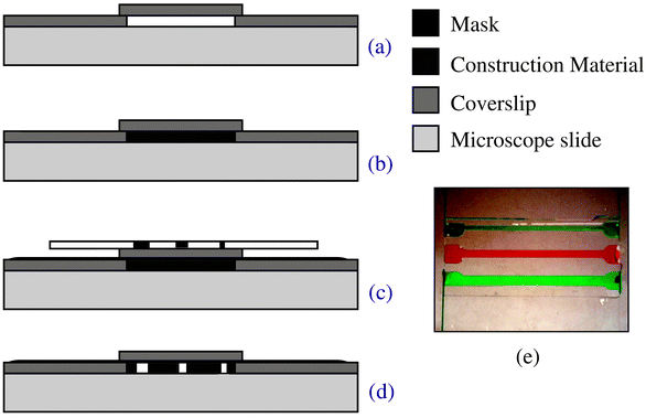 | ||
| Fig. 4 A glass cartridge (a) is constructed and filled with construction material (b). A mask is placed on top (c), and all layers are exposed to UV light. The resultant channels are flushed with methanol (d). A completed device with simple channel geometries (e) is shown. | ||
Construction material masters
In addition to making microfluidic devices directly using liquid phase methods, masters for PDMS micromolding can also be made in a few minutes using construction material. A small amount of the prepolymer (Fig. 5a) is placed on a silicon substrate, and a mask is positioned directly on the prepolymer solution (Fig. 5b). After exposure to UV light, the mask is pulled off the polymerized material, and the excess monomer is flushed away with methanol (Fig. 5c). At this point, the master can be baked for an hour to harden the construction material to make the master more durable for repeat use. PDMS is then poured and cured on top of the master.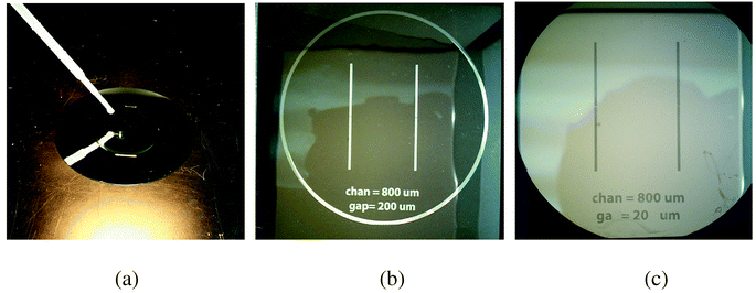 | ||
| Fig. 5 A small amount of construction material is applied to a silicon substrate (a). A photomask is placed on top of the fluid and exposed to UV light (b). The mask is peeled off, and the substrate is flushed with methanol and allowed to air dry (c). | ||
Results and discussion
Construction material is ideally suited for rapid microfluidic device fabrication. Low viscosity, optical patterning, and transparency are some of the properties that work well in the universal cartridge environment for filling, exposing, and visual observation. The universal cartridge concept offers maximum flexibility for fabrication, device iteration, and fluidic interconnection. Construction material can also be used to produce masters for PDMS micromolding offering advantages over commonly used photoresists.There are many factors that influence the quality of optical patterning of the construction material. Exposure time, intensity, and UV source are important parameters in the polymerization process. Typical exposure times in the universal cartridge were 30 s using a handheld UV lamp with an average UV intensity of 4 mW cm−2 at a distance of 1.5 cm. Shorter time was needed with a higher intensity source. The resolution of the construction material was determined by using a test mask that consisted of lines of varying widths and a series of squares with multiple gap separations. Minimum line widths and spaces of 25 μm were obtained (Fig. 6a,b) with a collimated UV source. Resolution of the structures is limited by the mask resolution and the collimation of the UV source. The ultimate limits on resolution will also be constrained by diffusion, device depth, and other optical effects. Thus, the resolution will never approach the resolution of standard resists (i.e. sub micron). However, for many microfluidic applications cost, not resolution, will likely be the driving parameter in commercialization. It should be noted that higher resolution optical patterning of the liquid phase is possible using expensive methods such as two-photon illumination.8 These techniques could be adapted to this platform for special applications requiring high-resolution features.
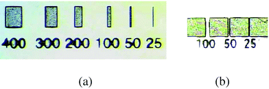 | ||
| Fig. 6 Line widths of 25 μm (a) and feature spacing of 25 μm (b) were successfully fabricated. | ||
The use of the commercially available polycarbonate/gasket pieces facilitates the URP concepts. Making a blank (or empty) universal cartridge is quick and easy. Many cartridges can be made in less than an hour since all that is required is to press the gasket material onto a slide and apply heat for 15 s. The whole process takes approximately 30 s. Occasionally, bubbles were observed when filling the cartridges with construction material. Slowly filling the cartridge and allowing capillary action to occur without any excess injection pressure minimized bubble formation. Remaining bubbles can also be removed by gently lifting one of the filling ports of the polymeric top with a tweezers tip. Bubbles that do not interfere with the device geometry can be ignored.
Since the cartridges are made on standard microscope slides, visualization and alignment using standard optical microscopy can be used to fabricate smaller components9,10 inside the channels. The cartridges are also compatible with current work being done on actuators and sensors made out of responsive hydrogel material.11 If hydrogel components inside the channel have a large degree of swelling, the top can be forcefully delaminated. Clamping the top reduces the risk of delamination if component swelling becomes a problem. Typically, component integration has been difficult when different materials and processes are needed. Different processes are not needed when all components are formed with the same liquid phase photopolymerization techniques. The universal cartridge concept allows integration of different components with varying functions into the same platform. In addition, once the cartridge is formed, filling, exposing, flushing and component integration can be easily automated for mass production. The glass cartridge has its own unique advantages. During filling, small amounts of construction material wick between the layers of coverslip and cement the layers together during the exposure step. No pre-assembly or bonding of a blank cartridge is necessary because the cartridge is being formed as the construction material is polymerized. Once the whole device has been exposed, the channels are flushed and the device is ready for filling. Different size coverslip glass can be used so that the overall size of the cartridge is flexible, and the thickness of the coverslip glass determines the channel height.
Inherent in any photopolymerization process is shrinkage of the material. This shrinkage can lead to a loss of adhesion and leakage. The advantage of using a flexible polymer top for the universal cartridge is that the flexibility of the polycarbonate film can accommodate the shrinkage. The polycarbonate film also transmits UV light, and the thin film layer (180 μm) does not degrade mask resolution significantly. The top material is not limited to polycarbonate film as other thin plastic films that are UV transparent could also be used.
Another advantage to the universal cartridge is that the outer dimensions do not change, only the channel network being fabricated. By keeping the filling holes on the top layer of consistent size and location, photomasks with device iterations can be made in advance. Since many masks can be made on one sheet of high-resolution film, device iteration can be made on the mask before the devices are fabricated. During the testing phase, the masks can be used as determined by the application of the device. A mask library (Fig. 7a) can be assembled with any number of design iterations. In addition, the masks can be ‘mixed and matched’ by forming single channels or by forming one half of the device and then the other half based on the needs of the target application (Fig. 7b). Alignment of the masks with the filling ports is made visually without the use of magnification, and slight misalignment does not affect the performance of the device for typical applications as long as a fluidic pathway is maintained. Additionally, not all of the filling ports need to be used. Unused ports can be plugged during the polymerization process. If more filling ports are needed, a 1/16th hole punch can be used to introduce more holes in the top layer.
 | ||
| Fig. 7 A mask library (a) can hold many channel designs and configurations. Mix and match masks (b) can be assembled to change the channel pattern by polymerizing two sides independently. | ||
Reliable fluidic connection to the cartridge is essential. Flexible EVA tubing attaches with no leakage to cored PDMS devices.4 However, PDMS does not adhere readily to polycarbonate or to the gasket material (i.e. double-sided adhesive). The nitrocellulose filter was essential in adhering the PDMS to the double-sided adhesive. The filter material cannot be removed from the adhesive once they are in contact. During potting and curing, the PDMS flows into the porous filter material forming a solid bond. The multilayer adhesive material used to make the connectors provided excellent adhesion to the polycarbonate top. In most cases, the devices leak before the connectors fail. The surface that the adhesive attaches to must be clean and free of any unpolymerized monomer, or leakage will occur immediately. There is no interference with mask alignment because the connectors are attached after the polymerization process. The low profile allows easy viewing under a microscope (see Fig. 8a). The tubing fits snugly into the cored PDMS, and there is low dead volume if the tubing is pushed close to the channel opening. In addition, luer hosebarbs can be inserted into the cored PDMS for luer type connections (Fig. 8b).
 | ||
| Fig. 8 Low profile connectors (a) allow for easy viewing under a microscope. Luer connects (b) can be placed in the connectors if desired. | ||
The process used for PDMS micromolding requires that a master be created that is the inverse of the final channel/device geometry. Masks for micromolding are typically constructed using photoresists, chemical/plasma etching, or electroplating. All these processes require hours of processing time. Using the URP methods described above to create masters for micromolding significantly reduces the design iteration time for traditional micromolding processes. In addition, liquid phase photopolymerization allows for the formation of multiple layers on the same master in minutes. An example of this technique is a microfluidic device for embryo manipulation and culture.12 The first layer of the master contains an oval region with thin strips that are roughly 100 μm wide. Reapplying construction material to the substrate and polymerizing again with the appropriate mask forms the second layer. The overall pattern consists of a channel with a gap of about 200 μm dividing the channel in two parts. A micrograph of the URP master and the resultant PDMS molded device is shown in Fig. 9. The liquid phase construction material replanarizes each layer because of the nature of the liquid as compared to physical deposition (i.e. vacuum deposition). A second layer using liquid phase construction methods could also be used in combination with physical deposition techniques.
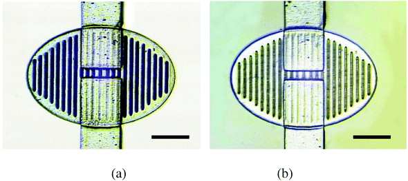 | ||
| Fig. 9 A construction material master (a) was fabricated on a Si wafer. A PDMS micromolded replica of the master (b) is shown. Scale bars are 1 mm. | ||
Comparisons between the construction material and EPON are shown in Table 1. Both construction material and EPON are negative photoresists and have similar properties with regards to sidewall angle, contact angle and adhesion to PDMS. Baking of the construction material at 50–75 °C for at least two hours was shown to make the polymer substantially harder and improves adhesion. Construction material allows one to make large-scale structures without noticeable cracking due to the low stress of the material as compared to EPON. However, height control is more difficult with construction material because it is processed directly in the liquid phase. Machined spacers were used to minimize this problem, but other adjustable alignment systems could also address this issue effectively. For very thin layers, excessive exposure of the construction material to oxygen inhibits polymerization, thus, a nitrogen atmosphere is needed to optimize URP performance. However, all of the work presented in this paper was performed in an air environment. The aspect ratio is smaller in construction material than in EPON, but solvent resistance and polymer shrinkage is similar.
| Construction material | EPON SU-8 50 | |
|---|---|---|
| a After exposure, development and post-bake. | ||
| Orientation | Negative | Negative |
| Sidewall angle | 80° ± 10° | 90° |
| Contact angle (with water) | 60° | 75° |
| Adhesion to PDMS | Low | Low |
| Adhesion to substrate | Good | Good |
| Master durability | Good | Good |
| Young’s modulus | 450–600 MPa | 4 GPa |
| Aspect ratio | 4–8 | 15 |
| Solvent resistance | Acetone, MeOH, IPA | Acetone, MeOH, IPAa |
| Polymer shrinkage | 10% | 7.5% |
Commercial epoxies (e.g. Norland 61 epoxy, Norland, New York) or other photopolymerizable materials can be used with URP methods. IBA monomer was chosen as our base construction material because it exhibits good resistance to chemical exposure (methanol, ethanol, isoproponol). The construction material also offers relatively low shrinkage during polymerization.
Conclusion
Emerging applications for microfluidic systems may not require the high-resolution capability of traditional MEMS methods. A more dominant factor than resolution will be the ease of integration of multiple functions into a low cost system. With URP, there is no high initial cost as compared to injection molding, and the process is easily integrated into a manufacturing environment. URP provides a low-cost alternative for making and integrating fluidic channels, requiring no prior experience in microfabrication techniques, no cleanroom facilities, and no expensive equipment. Liquid phase photopolymerization can be used as a platform for making devices that eliminate the need for micromolding and bonding and is compatible with component fabrication. In addition, URP can be used to create masters for PDMS micromolding quickly and economically using equipment already available in a standard laboratory environment (e.g. hot plate, scale, UV source). The low cost and high integration allows a manufacturing environment to incorporate ‘add-on fluidics’. For example, one could use the methods presented here to add microchannel networks directly onto substrates like silicon or circuit boards that already contain electronics or optics. URP complements both traditional MEMS processes and rapid prototyping when a fast turnaround is desired. The ability to rapidly iterate and build microfluidic systems in minutes instead of hours or days will continue to expand the potential of microfluidic systems.Acknowledgements
The authors would like to thank Buck Johnson for conducting Young’s modulus tests on the construction material and Glenn Walker for help in preparing this manuscript. This research was funded by DARPA-MTO.References
- Y. Xia and G. Whitesides, Angew. Chem., Int. Ed. Engl., 1998, 37, 550–575 CrossRef CAS.
- S. R. Quake and A. Scherer, Science, 2000, 290, 1536 CrossRef CAS.
- D. Duffy, J. C. McDonald, O. J. A. Schueller and G. Whitesides, Anal. Chem., 1998, 70(23), 4974–4984 CrossRef CAS.
- B.-H. Jo, L. M. V. Lerberghe, K. Motsegood and D. Beebe, J. MEMS, 2000, 9, 76–81 Search PubMed .
![[*]](https://www.rsc.org/images/entities/char_e103.gif) This paper demonstrated stackable and self-aligning PDMS layers.
This paper demonstrated stackable and self-aligning PDMS layers. - P. Mitchell, Nature Biotechnology, 2001, 19, 717 CrossRef CAS.
- G. Whitesides and A. Stroock, Phys. Today, 2001, 54(6), 42–47 CrossRef CAS.
- D. J. Beebe, J.S. Moore, Q. Yu, R. H. Liu, M. L. Kraft, B.-H. Jo and C. Devadoss, Proc. Natl. Acad. Sci. USA, 2000, 97(6), 13488 CrossRef CAS.
- S. Kawata, H.-B. Sun, T. Tanaka and K. Takada, Nature, 2001, 412, 697–698 CrossRef CAS.
- D. Beebe, J. S. Moore, J. M. Bauer, Q. Yu, R. H. Liu, C. Devadoss and B.-H. Jo, Nature, 2000, 404, 588–590 CrossRef CAS .
This paper outlined the basis for the development of ultra rapid prototyping and demonstrated sensors and actuators that are readily integrated with the authors′ work.
- D. J. Beebe, G. Mensing, J. Moorthy, C. Khoury and T. Pearce, Alternative approaches to microfluidic systems design, construction, and operation, in μTAS 2001, Monterey, CA, 2001 Search PubMed.
- Q. Yu, J. Bauer, J. Moore and D. Beebe, Appl. Phys. Lett., 2001, 78(17), 2589–2591 CrossRef CAS.
- H. C. Zeringue, K. R. King, I. K. Glasgow, S. Raty, M. B. Wheeler and D. J. Beebe, Zona pellucida removal of mammalian embryos in a microfluidic system, in Micro Total Analysis Systems, Kluwer Academic Publishers, Enschede, the Netherlands, 2000 Search PubMed.
| This journal is © The Royal Society of Chemistry 2002 |