
 Open Access Article
 This Open Access Article is licensed under a
 Creative Commons Attribution 3.0 Unported Licence
Enhanced photoresponse of ZnO quantum dot-decorated MoS2 thin films†
Ghazanfar Nazira,
M. Farooq Khana,
Imtisal Akhtarb,
Kamran Akbara,
Praveen Gautama,
Hwayong Noha,
Yongho Seo b,
Seung-Hyun Chuna and
Jonghwa Eom*a
b,
Seung-Hyun Chuna and
Jonghwa Eom*a
aDepartment of Physics & Astronomy, Graphene Research Institute, Sejong University, Seoul 05006, Korea. E-mail: eom@sejong.ac.kr
bDepartment of Nanotechnology & Advanced Materials Engineering, Graphene Research Institute, Sejong University, Seoul 05006, Korea
First published on 17th March 2017
Abstract
Transition metal dichalcogenides (TMDs) have been attracting attention because of their applications in optoelectronics and photo-detection. A widely used TMD semiconductor is molybdenum disulfide (MoS2), which has tremendous applications because of its tunable bandgap and high luminescence quantum efficiency. This paper reports on high photo responsivity (Rλ ∼ 1913 A W−1) of MoS2 photodetector by decorating a thin layer of zinc oxide (ZnO) quantum dots (ZnO-QDs) on MoS2. Results show that Rλ increases dramatically to 2267 A W−1 at Vbg = 30 V. The high response of ZnO-QDs/MoS2 heterostructures is attributed to a number of factors, such as effective charge transfer between ZnO-QDs and MoS2 surface and re-absorption of light photon resulting in production of electron–hole pairs.
Introduction
Photovoltaic cells, photodetectors, sensors, light-emitting diodes (LEDs), and LED displays will eventually require optoelectronic materials that demonstrate more efficient characteristics than those currently used. Graphene is an emergent material, which has been widely studied1–3 because of its promising properties, such as high mobility, ultra-thinness, and flexibility.4,5 Graphene has been extensively used in photodetection,6 bioelectronics,7 optoelectronics,8 and gas sensing.9Transition metal dichalcogenide (TMD) thin films have been used in the development of nano- and opto-electronic devices, such as ambipolar and high-quality field-effect transistors,10,11 digital integrated circuits,12 electric double-layer transistors,13 and highly responsive14 photodetectors.15 TMD materials have been widely investigated through theoretical or experimental studies, such as the investigation on charge transfer and photon–exciton interactions.16–21 One of the basic methods to tune the optical properties of TMDs involves controlling the charge carrier density. One of the mostly used TMD materials that has been widely investigated is molybdenum disulfide (MoS2). Different methods used to inject charge carriers in TMDs were intensively studied; these methods include tuning of charge carriers by using back gate voltage,22 O2 and H2O molecule adsorption,23,24 chemical process of molecule interaction,25 and plasmonic hot electron doping.26 Thus, finding a suitable means of efficient doping to achieve superior optical properties of TMDs is necessary.
Semiconductor quantum dots (QDs) demonstrate unique behaviors, such as size-tunable atomic-like characteristics resulting from quantum confinement in the nanometer scale. A number of semiconductors consisting of QDs have been widely used in different research fields because of their anomalous behavior. Groups II–VI semiconductor QDs, such as CdSe and ZnSe,27,28 displays an advantage over IV and III–V materials29–31 due to their higher exciton energies and the stronger phonon–exciton interaction among them. Unfortunately, the bandgap of CdSe in bulk form is 1.74 eV, which is very difficult to tune in the ultraviolet (UV) region. Moreover, CdSe is toxic and unsafe for medical applications. On contrary, ZnSe can be used in UV-blue range of energies. However, ZnSe-based devices demonstrate less efficient performance because of certain defects. Zinc oxide (ZnO), which displays a wide direct bandgap of 3.37 eV at room temperature, is a good candidate for short wavelength applications. ZnO has become famous as the brightest emitter among available wide-bandgap semiconductors because of its high exciton energy (∼60 meV).32 In addition, ZnO is low cost and exhibits high resistance to defects, high stability, environment friendly characteristics, and biosafety. Based on these characteristics, ZnO-QDs are advantageous over CdSe-QDs and ZnSe-QDs in terms of practical applications.33,34
This study comparatively explored the photoresponse of pristine MoS2 and ZnO-QDs/MoS2 heterostructures. We investigated a number of electrical and photoelectrical properties, such as carrier mobility, responsivity (Rλ), detectivity (D*), external quantum efficiency, and linear dynamic range with and without ZnO-QDs. All of these parameters were investigated at various back gate voltages (Vbg). High carrier mobility when ZnO-QDs is deposited over MoS2 is caused by reduced carrier transit time (the time required for an electron or other charge carrier to travel between two electrodes in a transistor) within a field-effect transistor (FET). Moreover, rise and decay times of carriers in a photodetector was calculated, and the results showed that after ZnO-QDs interacted with pristine MoS2, the decay time dramatically changed suggesting the efficient charge transfer that occurred between ZnO-QDs and MoS2 surface. Furthermore, this work discusses the proposed mechanism of charge transfer between ZnO-QDs and pristine MoS2.
Experimental section
Sample preparation
Naturally available MoS2 was mechanically exfoliated using the scotch tape method over a heavily p-doped Si as substrate with 300 nm-thick SiO2 as capping layer. The desired flake with a suitable thickness was chosen by using an optical microscope. A large Cr/Au pattern with a thickness of 6/30 nm was subsequently deposited around the desired flake by using photolithography. To make source and drain contacts, we performed e-beam lithography, followed by the final deposition of an 8/80 nm-thick Cr/Au in an evaporation chamber, in which a high vacuum of 2 × 10⁻⁶ Torr was maintained. Electrical measurements using Keithley 2400 Source Meter and Keithley 6485K Picoammeter were subsequently performed by placing the sample in a vacuum at room temperature. To study photoresponse, we placed our sample in a vacuum and illuminated by deep UV light (DUV) with an intensity of 11 mW cm−2 and a wavelength of 220 nm. Structural investigation and material identification were performed using Raman spectroscopy and atomic force microscopy (AFM). Fig. S1† shows the results of the Raman analysis of our flake, and the results confirm the multilayer nature of MoS2 with peaks located in exactly the same positions as described in a number of publications. Laser wavelength was obtained at 514 nm, and a low power of less than 1 mW was chosen to avoid structural degradation caused by heating effects of laser. The size of laser spot used in Raman spectroscopy is 0.7 μm. Fig. S2† shows the AFM micrograph of MoS2, and the image confirms the multilayer nature of MoS2 which is 7 nm thick (∼11 layers).Synthesis and characterization of ZnO QDs
ZnO-QDs were synthesized in methanol via hydrolysis method. Typically, 20 mmol methanol solution of ZnAc2:2H2O was prepared and maintained at 60 °C followed by dropwise addition of 200 mmol methanol solution of KOH for 10 min under vigorous stirring for 2 h. Finally, the QDs were collected by centrifugation and then washed multiple times with methanol. The ZnO-QDs solution was drop casted over MoS2 photodetector device and then baked gently at 70 °C for 10 min. To confirm the nature of the material, we measured the excitation and emission of matrix (EEM) of ZnO-QDs by using a spectrofluorometer (Hitachi, F7000, Japan). The measured excitation/emission wavelength was adjusted to 220–500 nm/280–550 nm at a scan step of 5 and 1 nm for excitation and emission, respectively. Moreover, a polarized cut off filter of 290 nm was placed in front of a lamp to remove Rayleigh scattering, and Milli-Q water was used as blank and subtracted from the EEM of each sample.Results and discussion
Fig. 1a shows the 3D schematic of a photodetector consisting of ZnO-QDs decorated MoS2 as channel flake. The MoS2 is supported on SiO2/p+-Si wafer substrate with 300 nm-thick SiO2. Fig. 1b shows the optical image of the MoS2 FET with a channel length of 1.52 μm and a width of 6.34 μm.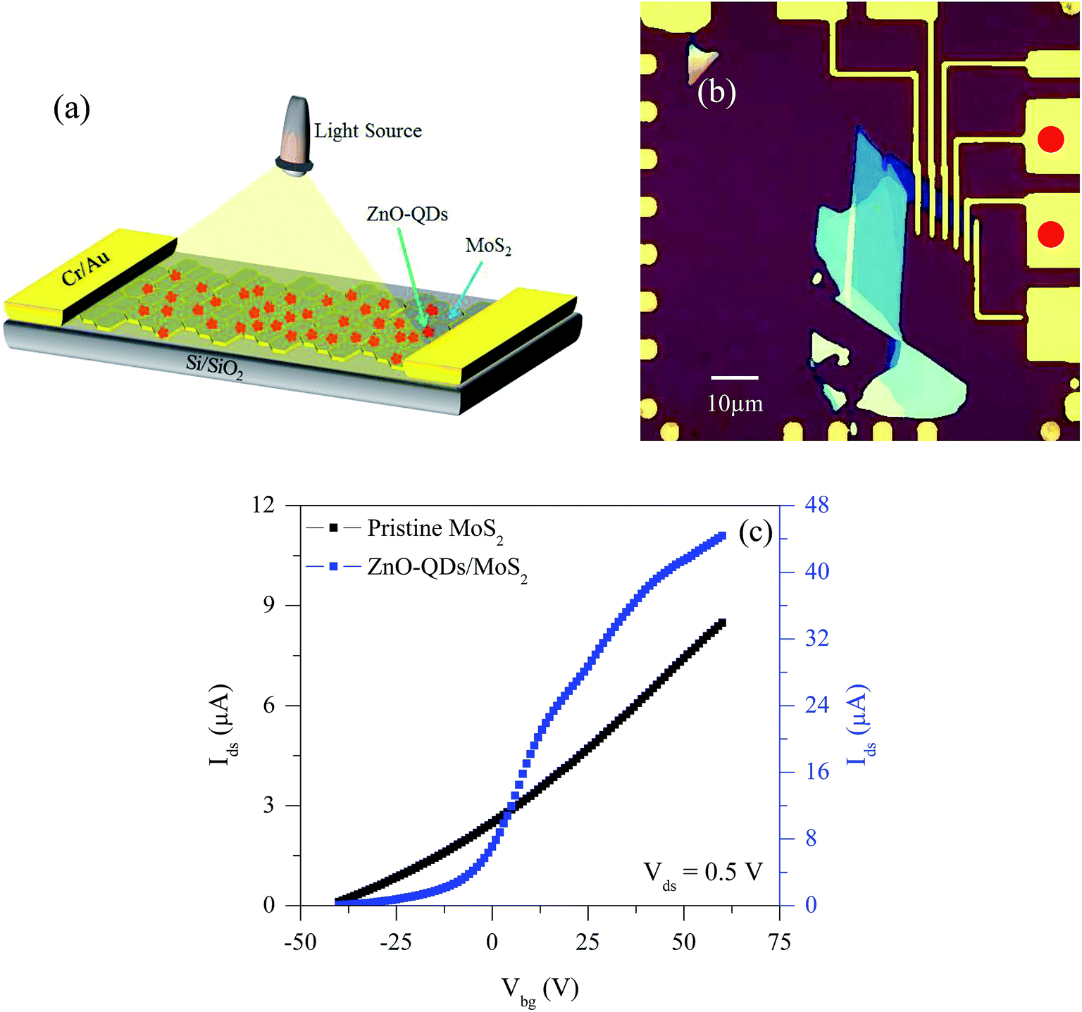 | ||
| Fig. 1 (a) 3D schematic of ZnO-QDs decorated MoS2 photodetector and (b) optical image of MoS2 (scale bar: 10 μm) consisting of a multilayer flake with Cr/Au = 8/60 nm contacts. Red circles represent the contacts for electrical measurements. (c) Ids versus Vbg graph for MoS2 photodetector measured at Vds = 0.5 V without and with ZnO-QDs. The mobility of pristine MoS2 and ZnO-QDs/MoS2 heterostructures are 5.75 and 25.09 cm2 V−1 s−1, respectively. | ||
Raman spectroscopy is the most useful tool utilized in non-destructive analysis of structural properties.35–42 We chose a desired flake by using an optical microscope and then performed Raman analysis to confirm flake thickness and to identify the material. The Raman spectra of the MoS2 flake were obtained at room temperature. Fig. S1† shows the Raman spectra for our MoS2 flake. The in-plane (E12g) and out-of-plane (A1g) vibrational modes for multilayer MoS2 (ML-MoS2) was found at ∼384 and ∼408 cm−1, respectively. The difference between E12g and A1g of the ML-MoS2 is ∼24 cm−1, consistent with previous results.43–45 The black curve represents pristine MoS2 and the red curve represents the ZnO-QDs/MoS2 heterostructures. The peak positions did not change after ZnO deposition. Fig. S2† shows the AFM images used to further confirm the thickness of the layer of the ML-MoS2 flake. The measured thickness of our flake is 7 nm (11-layer). We found that the average height of ZnO-QDs is 2–4 Å and the average width is 10–20 nm (Fig. S3†).
We determined the electrical characteristics under vacuum by applying Vbg. Transfer characteristics of pristine MoS2 and ZnO-QDs/MoS2 structures were examined and the results are shown in Fig. 1c. We maintained the drain–source voltage (Vds) at 0.5 V throughout our measurements. The drain current (Ids) increases after drop casting ZnO-QDs over MoS2 in positive gate voltage range while decrease in negative gate voltage because of increase in leakage current in that region. The field-effect mobilities can be calculated using the fundamental formula  , where L and W are the channel length (1.52 μm) and width (6.34 μm) of our MoS2 flake, respectively,
  is the slope of the linear region of transfer curves, and Cg is the gate capacitance (∼115 aF μm−2) of Si substrate with 300 nm-thick SiO2 as capping layer. Therefore, the field-effect mobilities are 5.75 and 25.09 cm2 V−1 s−1 before and after decorating ZnO-QDs on MoS2 flake, respectively.
Fig. 2a and b show the output (I–V) characteristics before and after drop casting ZnO-QDs over MoS2 surface. Output characteristics of pristine MoS2 show a linear relationship with Ids and Vds at different Vbg values, demonstrating that contacts (Cr/Au) on the surface of MoS2 are ohmic and that no Schottky barrier exists at the metal–semiconductor junction interface. Moreover, Fig. 2b shows the output characteristics after decorating ZnO-QDs over MoS2. The output characteristics again show ohmic nature of the contacts but with increased Ids, confirming that ZnO-QDs on the surface of MoS2 does not damage the contacts or cause structural deformation, which is beneficial for the applications of FET in opto-electronics.
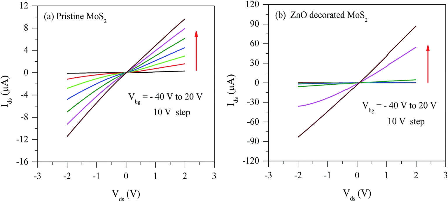 | ||
| Fig. 2 (a) Output characteristics (Ids–Vds) of pristine MoS2 at different Vbg values with equal steps of 10 V. (b) The corresponding (Ids–Vds) curves after ZnO-QDs decoration at the same Vbg showed an increase in current. The graphs in (a) and (b) show a linear trend, confirming the formation of ohmic contacts before and after decorating ZnO-QDs on MoS2. | ||
We further investigated MoS2 photodetectors by determining the time-dependent photoresponse of pristine MoS2 and ZnO-QDs/MoS2 heterostructures under varying Vbg values. To determine the photoresponse behavior of our device, we placed our device in a vacuum and illuminated by DUV in a way that light falls vertically on its surface with an effective area of 9.64 μm2. All measurements were performed at Vds = 0.5 V. As DUV light falls on MoS2 surface, the photocurrent (IPh) increases with increasing Vbg caused by the increase in carrier drift velocity and the corresponding reduction in carrier transit time (defined as Tt = L2/μVds,14 where μ is the field-effect mobility and L is the channel length). Our calculation showed that the carrier transit time for ZnO-QDs/MoS2 is lower than that for pristine MoS2. As a result, the current increases with increasing Vbg; thus, IPh becomes dominant over thermionic and tunneling currents at all Vbg values.46
IPh for pristine MoS2 and ZnO-QDs/MoS2 are shown in Fig. 3a and b, respectively, and IPh of ZnO-QDs/MoS2 is greater than that of pristine MoS2 at all Vbg values (0–30 V). This phenomenon was observed because in the case of ZnO-QDs/MoS2 heterostructures, ZnO-QDs provide surplus carriers to MoS2, and these carriers equally contribute to the increase in overall photoresponse behavior under DUV light.47 Another important parameter in evaluating devices under light illumination is Rλ. Rλ indicates the response of a device to light (specific wavelength) and is defined as “IPh produced per unit power of incident light on effective area of a photodetector”.46
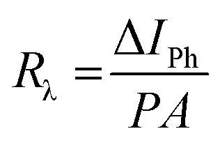 | (1) |
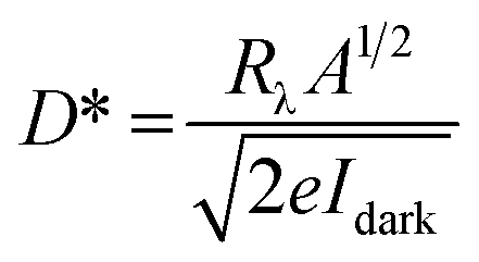 | (2) |
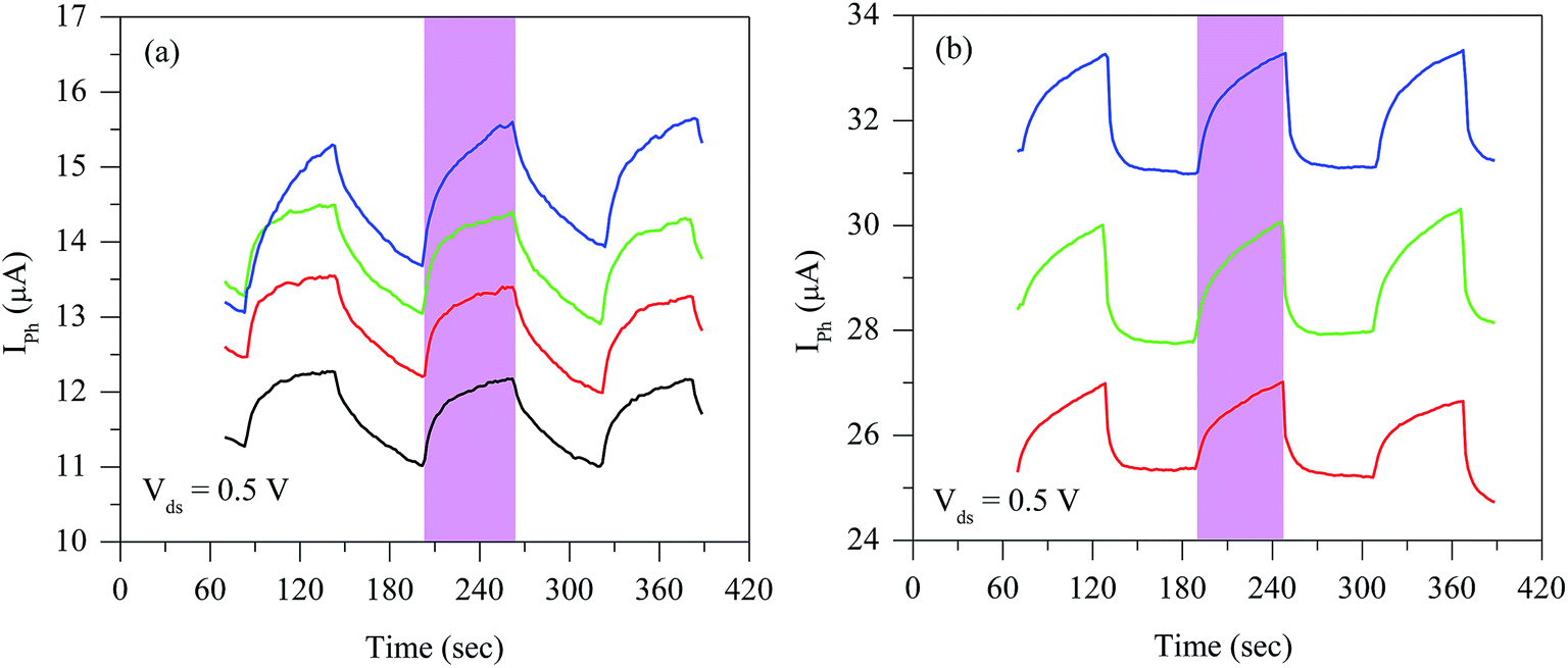 | ||
| Fig. 3 Photocurrent (IPh) versus time under different Vbg values ranging from Vbg = 0 V (black curve) to Vbg = 30 V (blue curve). Photoresponse of (a) pristine MoS2 measured at different Vbg values with equal steps of 10 V and Vds = 0.5 V under deep ultraviolet illumination with an intensity of 11 mW cm−2 and a wavelength of 220 nm with alternating on and off cycles. (b) The photoresponse of the same device after ZnO-QDs drop casting shows higher IPh at all Vbg values. The photoresponse at Vbg = 0 V has been omitted in order to see the clear interpretation of plot. | ||
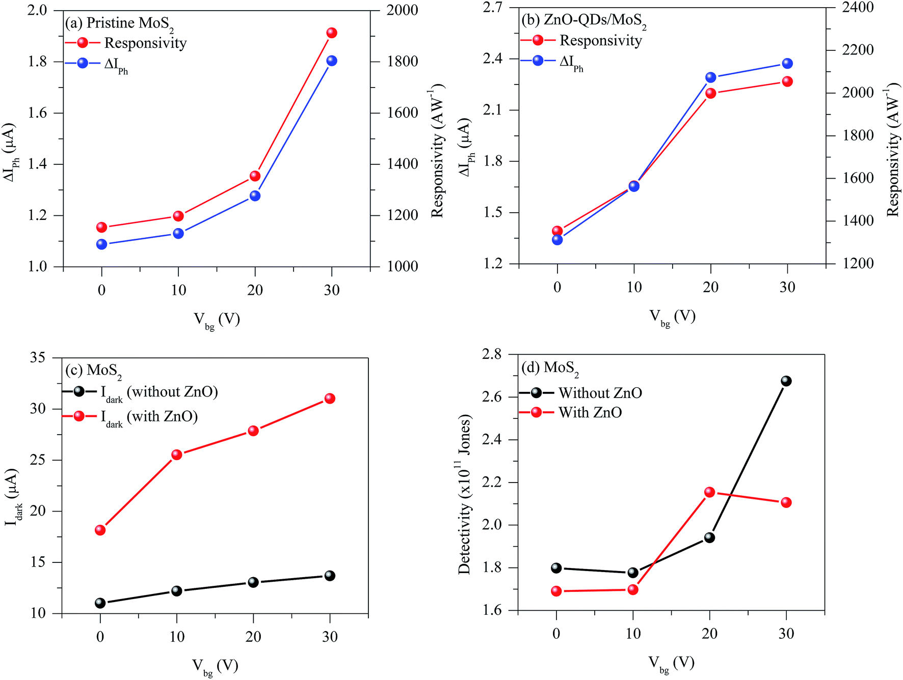 | ||
| Fig. 4 Photocurrent generation (ΔIPh) (in blue circles) and responsivity (Rλ) (in red circles) versus back gate voltage (Vbg) for (a) pristine MoS2 and (b) ZnO-QDs/MoS2 heterostructures; ΔIPh and Rλ both increased after decorating ZnO-QD on MoS2. (c) Dark current versus Vbg before and after ZnO-QD decoration. Dark current is higher in ZnO-QDs/MoS2 heterostructure than in pristine MoS2 at all Vbg values. (d) Detectivity (D*) versus Vbg before and after ZnO-QDs at a power of 1011 jones. Low value of D* at a low Vbg is caused by high dark current at these values. | ||
We prepared a schematic of energy band (Fig. 5) to illustrate photodetector behavior of our pristine MoS2. In the absence of light illumination and any Vds or Vbg, the device is at equilibrium state. When light with a wavelength of 220 nm falls on pristine MoS2 in its OFF state (Vbg = 0 V), light is absorbed by the pristine MoS2, resulting in the excitation of electrons to the conduction band even when Vbg was zero (Fig. 5b). A low number of charge carriers will move to the conduction band when Vbg < Vth and the drain current is very low (Fig. 5c). In contrast, in the ON state (Vbg > Vth), photo-generated, thermionic, and tunneling currents contribute cumulatively to IPh enhancement (Fig. 5d). Our devices showed good Rλ at room temperature relative to that of the reported devices.49,50
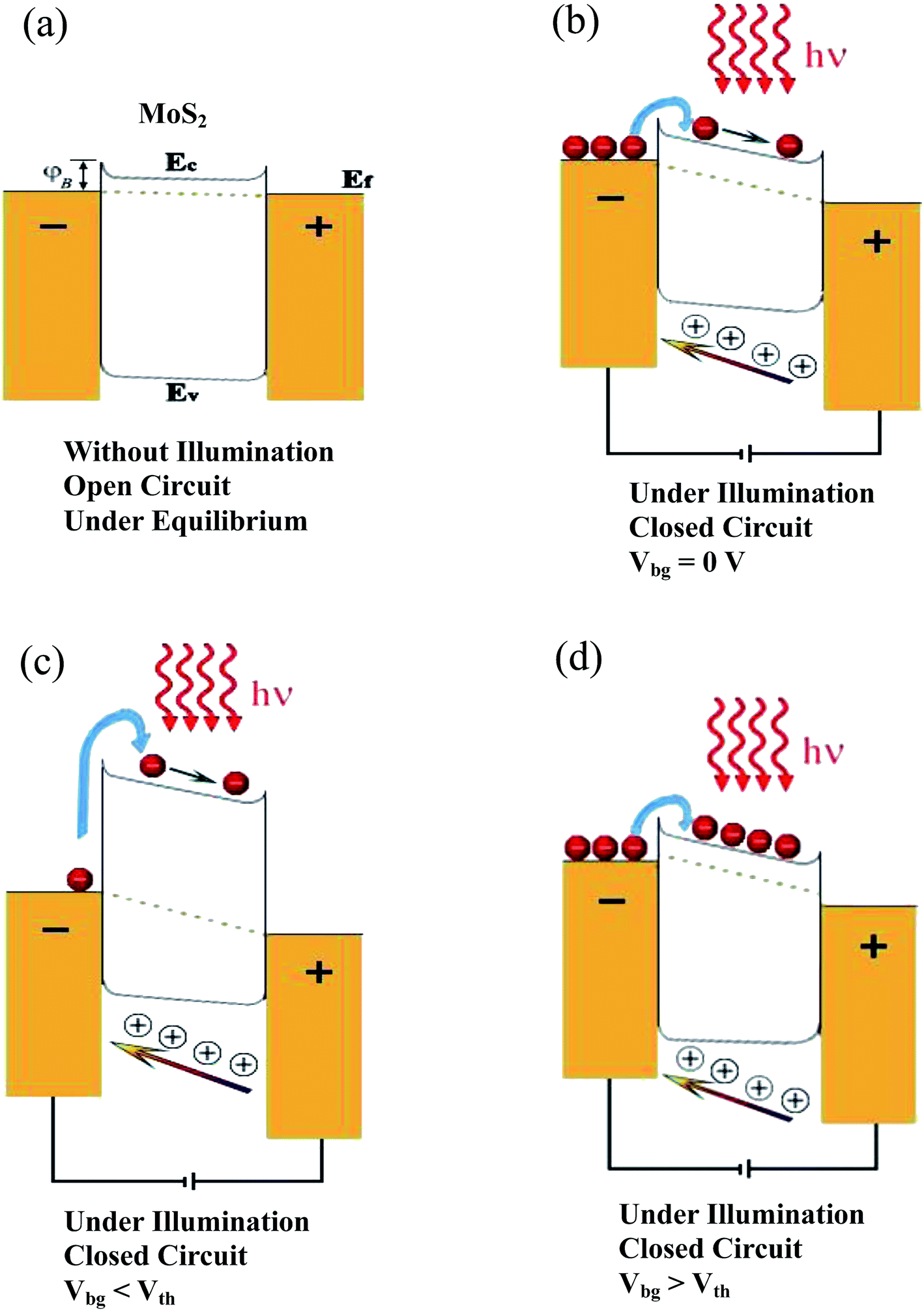 | ||
| Fig. 5 Schematic energy diagram in the absence of light and under illumination represent the energy barrier and mechanism of photocurrent (IPh) generation. Schematic energy diagram (a) in the dark and at drain–source voltage (Vds) = 0 V under equilibrium and (b) under light illumination at Vds ≠ 0 V and back gate voltage (Vbg) = 0. (c and d) IPh generation under light illumination at different Vbg values for Vbg < Vth and Vbg > Vth respectively by taking Vds ≠ 0 V. | ||
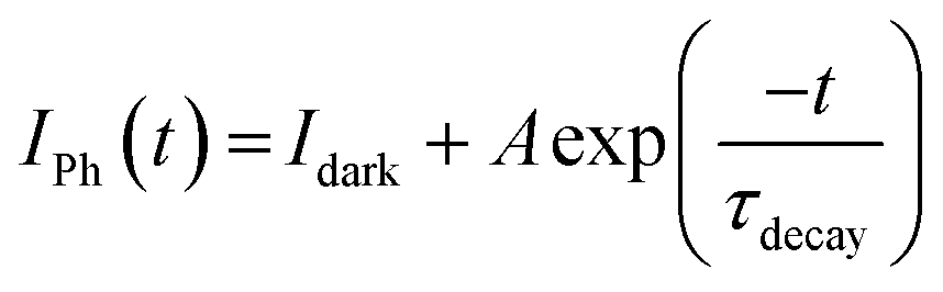
Dynamic response to light irradiation was studied, and the rise and decay times were measured by fitting the curves to exponential decay function51,52
 | (3) |
 | ||
| Fig. 6 Photocurrent (IPh) versus time at different back gate voltages (Vbg) ranging from Vbg = 0 V (red curve) to Vbg = 30 V (blue curve). (a) IPh relaxation for pristine MoS2 at different Vbg values in the absence of DUV light. (b) Dramatic increase in IPh relaxation for ZnO-QDs/MoS2 at all Vbg values. (c) Rise time for pristine MoS2 under DUV light at different Vbg values. (d) Rise time after ZnO-QDs decoration over MoS2. The data were fitted by eqn (3) and indicated by black lines in all graphs. | ||
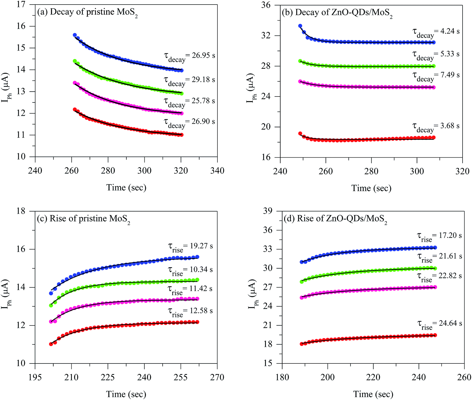
To understand the mechanism of IPh generation in our heterostructures, we prepared a schematic of energy band (Fig. 7). Fig. 7 shows the band bending and carrier transfer direction when ZnO-QDs and MoS2 interact with each other. The electron affinity56 of ML MoS2 is approximately 3.9 eV, which is comparable to that of ZnO-QDs. Our ML MoS2 film is 7 nm thick (∼11 layers) and its indirect bandgap56 is 1.2 eV, which is considerably smaller than the bandgap of ZnO-QDs (3.37 eV).58 Considering that both ZnO-QDs and MoS2 are n-type materials, we proposed energy band diagrams showing the bandgap before and after formation of heterostructures (Fig. 7a and b). Fermi level for ZnO-QDs is closer to vacuum level as compared with that for MoS2 (Fig. 7). Fig. 7a shows basic schematic for MoS2 and ZnO-QDs contains information about electron affinity and bandgap before their heterojunction. When MoS2 and ZnO-QDs interact to form heterostructures caused by van der Waals forces, we proposed that there exist number of ways of carrier injection between MoS2 and ZnO-QDs. When light falls on heterostructure, there occurs injection of electrons from ZnO-QDs conduction band into MoS2 conduction band as explained by process “V” in Fig. 7b and leads to increase in current. Also, some of the electrons in ZnO-QDs conduction band get energy from thermal agitation at room temperature and move to MoS2 conduction band as explained by process “III”. The electrons in the valence band also move from ZnO-QDs to MoS2 due to thermal agitation shown by process “IV”. The motion of electrons causes band bending,59 which is manifested as a small energy barrier. When these heterostructures are illuminated under DUV light, photo-generation occurs because both ZnO-QDs and MoS2 strongly absorb light photon and electrons move from valence to conduction band explained by process “I”. Also, some of the electrons in the conduction band move back to the valence band of ZnO-QDs and emit light photon which caught by electrons in the valence band of MoS2 and get excited toward conduction band of MoS2 explained by process “II”. IPh enhancement is generally caused by a large number electron–hole pairs, resulted from tunneling of electrons from ZnO-QDs to MoS2 surface. Given that the decay time of the heterostructures is shorter than that of pristine MoS2, the recombination rate and consequently the photoresponse is faster in ZnO-QDs/MoS2 than in pristine MoS2.
 | ||
| Fig. 7 (a) Energy diagram for MoS2 and ZnO quantum dots (QDs) before contact. (b) Energy diagram of the interface between MoS2 and ZnO-QDs after construction of heterojunction; different Roman numerals represent different proposed mechanisms of carrier transformation across junction, as well as between valence and conduction bands. (I) Shows photon excitation of charge carriers in MoS2 and ZnO-QDs; (II) indicates that carriers de-excite the photon emitted by ZnO-QDs and that the emitted photon is re-absorbed by MoS2; (III) electrons tunnel from ZnO-QDs to MoS2; (IV) holes transfer from ZnO-QDs to MoS2; and (V) electrons from ZnO-QDs are thermally agitated toward MoS2. | ||
Two more parameters, namely, external quantum efficiency (EQE) and linear dynamic response (LDR) were investigated to better assess the photodetector performance. These parameters were measured at different Vbg values without and with interaction of ZnO-QDs. EQE is given by the formula48
 | (4) |
 | (5) |
 ratios. In other words, the increase in dark current in ZnO-QDs/MoS2 heterostructures (Fig. 4c) degrades LDR.
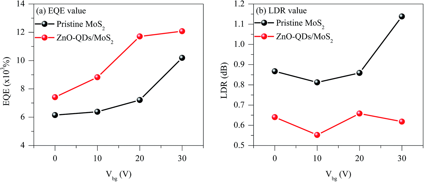 | ||
| Fig. 8 (a) External quantum efficiency (EQE) versus back gate voltage (Vbg) for pristine-MoS2 and ZnO-QDs/MoS2. EQE is high after ZnO decoration over MoS2. (b) Linear dynamic range (LDR) versus Vbg for pristine MoS2 and ZnO-QDs/MoS2. LDR decreases after ZnO-QD decoration at all Vbg values because of the increase in dark current as shown in Fig. 4c. | ||
To confirm the size of ZnO-QDs, we obtained an AFM image (Fig. S3†), which shows that the average height of ZnO-QDs is 2–4 Å and the average width is 10–20 nm. Moreover, we obtained a 3-D fluorescence plot by choosing a range of wavelength of light to be used to irradiate our samples (Fig. S4†). By using the formula Eg = hc/λ, we determined the height excitation peak at ∼378 nm, leading to a bandgap of 3.28 eV, which corresponds to the bandgap of our 10 nm ZnO-QDs.61 The EEM of ZnO-QDs was measured using a spectrofluorometer. The EEM clearly shows the maximum emission peak at approximately 440 nm at 378 nm excitation. The red thick line is caused by Raman scattering of ZnO-QDs dispersed in methanol solution.
Conclusion
We investigated for the first time a high-response photodetector based on MoS2/ZnO-QDs heterostructures. The junction between MoS2 and ZnO-QDs forms n–n type heterostructures, resulting in enhanced carrier mobility caused by injection of electrons from ZnO-QDs into MoS2. A number of factors were investigated. Rλ increased after ZnO-QDs were deposited over MoS2 surface, and this phenomenon resulted from the increase in IPh caused by the surplus carriers cumulatively transferred from ZnO-QDs to MoS2 surface. EQE increased after ZnO-QDs were drop casted over MoS2, whereas after decorating with ZnO-QDs, D* decreased caused by the massive increase in dark current. Moreover, LDR degradation corresponds to the increase in dark current in ZnO-QDs/MoS2 heterostructures. We extensively discussed the basic phenomenon of charge transfer in pristine MoS2 and ZnO-QDs/MoS2 heterostructures. In addition, this report presents a number of proposed factors that contribute to the increasing IPh resulting from generation of charge carriers across the junction of the ZnO-QDs and MoS2 surfaces. We suggest that generation of charge carriers, which contribute to IPh enhancement, is affected by the five parameters mentioned above (Fig. 7). This high photoresponse is largely caused by the effect of light–matter interactions based on tunneling of photo-excited carriers from ZnO-QDs to MoS2 and by re-absorption of emitted photons from ZnO-QDs by MoS2. Our work describes the basic mechanism of charge transfer between ZnO-QDs and MoS2.Acknowledgements
This research was supported by Nano-Material Technology Development Program (2012M3A7B4049888) through the National Research Foundation of Korea (NRF) funded by the Ministry of Science, ICT and Future Planning. This research was also supported by Priority Research Center Program (2010-0020207) and the Basic Science Research Program (2016R1D1A1A09917762) through NRF funded by the Ministry of Education.References
- N. Mohanty and V. Berry, Graphene-based single-bacterium resolution biodevice and DNA transistor: interfacing graphene derivatives with nanoscale and microscale biocomponents, Nano Lett., 2008, 8(12), 4469–4476 CrossRef CAS PubMed.
- S. Rumyantsev, G. Liu, M. S. Shur, R. A. Potyrailo and A. A. Balandin, Selective gas sensing with a single pristine graphene transistor, Nano Lett., 2012, 12(5), 2294–2298 CrossRef CAS PubMed.
- C.-H. Liu, Y.-C. Chang, T. B. Norris and Z. Zhong, Graphene photodetectors with ultra-broadband and high responsivity at room temperature, Nat. Nanotechnol., 2014, 9(4), 273–278 CrossRef CAS PubMed.
- F. Schwierz, Graphene transistors, Nat. Nanotechnol., 2010, 5(7), 487–496 CrossRef CAS PubMed.
- A. K. Geim and K. S. Novoselov, The rise of graphene, Nat. Mater., 2007, 6(3), 183–191 CrossRef CAS PubMed.
- J. Park, Y. Ahn and C. Ruiz-Vargas, Imaging of photocurrent generation and collection in single-layer graphene, Nano Lett., 2009, 9(5), 1742–1746 CrossRef CAS PubMed.
- L. H. Hess, M. Seifert and J. A. Garrido, Graphene transistors for bioelectronics, Proc. IEEE, 2013, 101(7), 1780–1792 CrossRef CAS.
- F. Bonaccorso, Z. Sun, T. Hasan and A. Ferrari, Graphene photonics and optoelectronics, Nat. Photonics, 2010, 4(9), 611–622 CrossRef CAS.
- Y. Liu, J. Chang and L. Lin, in A flexible graphene FET gas sensor using polymer as gate dielectrics, 2014 IEEE 27th International Conference on Micro Electro Mechanical Systems (MEMS), IEEE, 2014, pp. 230–233 Search PubMed.
- V. Podzorov, M. Gershenson, C. Kloc, R. Zeis and E. Bucher, High-mobility field-effect transistors based on transition metal dichalcogenides, Appl. Phys. Lett., 2004, 84(17), 3301–3303 CrossRef CAS.
- B. Radisavljevic and A. Kis, Mobility engineering and a metal–insulator transition in monolayer MoS2, Nat. Mater., 2013, 12(9), 815–820 CrossRef CAS PubMed.
- H. Wang, L. Yu, Y.-H. Lee, Y. Shi, A. Hsu, M. L. Chin, L.-J. Li, M. Dubey, J. Kong and T. Palacios, Integrated circuits based on bilayer MoS2 transistors, Nano Lett., 2012, 12(9), 4674–4680 CrossRef CAS PubMed.
- Y. Zhang, J. Ye, Y. Yomogida, T. Takenobu and Y. Iwasa, Formation of a stable p–n junction in a liquid-gated MoS2 ambipolar transistor, Nano Lett., 2013, 13(7), 3023–3028 CrossRef CAS PubMed.
- O. Lopez-Sanchez, D. Lembke, M. Kayci, A. Radenovic and A. Kis, Ultrasensitive photodetectors based on monolayer MoS2, Nat. Nanotechnol., 2013, 8(7), 497–501 CrossRef CAS PubMed.
- Z. Yin, H. Li, H. Li, L. Jiang, Y. Shi, Y. Sun, G. Lu, Q. Zhang, X. Chen and H. Zhang, Single-layer MoS2 phototransistors, ACS Nano, 2011, 6(1), 74–80 CrossRef PubMed.
- Q. H. Wang, K. Kalantar-Zadeh, A. Kis, J. N. Coleman and M. S. Strano, Electronics and optoelectronics of two-dimensional transition metal dichalcogenides, Nat. Nanotechnol., 2012, 7(11), 699–712 Search PubMed.
- S. Z. Butler, S. M. Hollen, L. Cao, Y. Cui, J. A. Gupta, H. R. Gutierrez, T. F. Heinz, S. S. Hong, J. Huang and A. F. Ismach, Progress, challenges, and opportunities in two-dimensional materials beyond graphene, ACS Nano, 2013, 7(4), 2898–2926 CrossRef CAS PubMed.
- Z. J. Qi, J. A. Rodríguez-Manzo, A. s. R. Botello-Méndez, S. J. Hong, E. A. Stach, Y. W. Park, J.-C. Charlier, M. Drndić and A. C. Johnson, Correlating atomic structure and transport in suspended graphene nanoribbons, Nano Lett., 2014, 14(8), 4238–4244 Search PubMed.
- C. Cong, J. Shang, X. Wu, B. Cao, N. Peimyoo, C. Qiu, L. Sun and T. Yu, Synthesis and Optical Properties of Large-Area Single-Crystalline 2D Semiconductor WS2 Monolayer from Chemical Vapor Deposition, Adv. Opt. Mater., 2014, 2(2), 131–136 CrossRef.
- A. Rubio, Hybridized graphene: nanoscale patchworks, Nat. Mater., 2010, 9(5), 379–380 CrossRef CAS PubMed.
- Q. Tang and Z. Zhou, Graphene-analogous low-dimensional materials, Prog. Mater. Sci., 2013, 58(8), 1244–1315 CrossRef CAS.
- J. S. Ross, S. Wu, H. Yu, N. J. Ghimire, A. M. Jones, G. Aivazian, J. Yan, D. G. Mandrus, D. Xiao and W. Yao, Electrical control of neutral and charged excitons in a monolayer semiconductor, Nat. Commun., 2013, 4, 1474 CrossRef PubMed.
- S. Tongay, J. Zhou, C. Ataca, J. Liu, J. S. Kang, T. S. Matthews, L. You, J. Li, J. C. Grossman and J. Wu, Broad-range modulation of light emission in two-dimensional semiconductors by molecular physisorption gating, Nano Lett., 2013, 13(6), 2831–2836 Search PubMed.
- H. Nan, Z. Wang, W. Wang, Z. Liang, Y. Lu, Q. Chen, D. He, P. Tan, F. Miao and X. Wang, Strong photoluminescence enhancement of MoS2 through defect engineering and oxygen bonding, ACS Nano, 2014, 8(6), 5738–5745 CrossRef CAS PubMed.
- S. Mouri, Y. Miyauchi and K. Matsuda, Tunable photoluminescence of monolayer MoS2 via chemical doping, Nano Lett., 2013, 13(12), 5944–5948 CrossRef CAS PubMed.
- Y. Kang, S. Najmaei, Z. Liu, Y. Bao, Y. Wang, X. Zhu, N. J. Halas, P. Nordlander, P. M. Ajayan and J. Lou, Plasmonic hot electron induced structural phase transition in a MoS2 monolayer, Adv. Mater., 2014, 26(37), 6467–6471 CrossRef CAS PubMed.
- I. Suemune, T. Tawara, T. Saitoh and K. Uesugi, Stability of CdSe and ZnSe dots self-organized on semiconductor surfaces, Appl. Phys. Lett., 1997, 71(26), 3886–3888 CrossRef CAS.
- N. Myung, Y. Bae and A. J. Bard, Effect of surface passivation on the electrogenerated chemiluminescence of CdSe/ZnSe nanocrystals, Nano Lett., 2003, 3(8), 1053–1055 CrossRef CAS.
- A. Malachias, R. Magalhães-Paniago, S. Kycia and D. G. Cahill, X-ray study of strain and composition of Si/Ge0. 85Si0. 15(111) islands grown in Volmer–Weber mode, J. Appl. Phys., 2004, 96(6), 3234–3238 CrossRef CAS.
- A. Tsatsul’nikov, A. Kovsh, A. Zhukov, Y. M. Shernyakov, Y. G. Musikhin, V. Ustinov, N. Bert, P. Kop’ev, Z. I. Alferov and A. Mintairov, Volmer–Weber and Stranski–Krastanov InAs-(Al, Ga) As quantum dots emitting at 1.3 μm, J. Appl. Phys., 2000, 88(11), 6272–6275 CrossRef.
- S. Fafard, D. Leonard, J. Merz and P. Petroff, Selective excitation of the photoluminescence and the energy levels of ultrasmall InGaAs/GaAs quantum dots, Appl. Phys. Lett., 1994, 65(11), 1388–1390 CrossRef CAS.
- Z. Tang, G. K. Wong, P. Yu, M. Kawasaki, A. Ohtomo, H. Koinuma and Y. Segawa, Room-temperature ultraviolet laser emission from self-assembled ZnO microcrystallite thin films, Appl. Phys. Lett., 1998, 72(25), 3270–3272 CrossRef CAS.
- Z. L. Wang, Zinc oxide nanostructures: growth, properties and applications, J. Phys.: Condens. Matter, 2004, 16(25), R829 CrossRef CAS.
- J. Lu, Z. Ye, Y. Zhang, Q. Liang, S. Fujita and Z. Wang, Self-assembled ZnO quantum dots with tunable optical properties, Appl. Phys. Lett., 2006, 89(2), 023122 CrossRef.
- D. J. Late, Temperature dependent phonon shifts in single-layer WS2, ACS Appl. Mater. Interfaces, 2014, 6(2), 1158–1163 Search PubMed.
- D. J. Late, S. N. Shirodkar, U. V. Waghmare, V. P. Dravid and C. Rao, Thermal Expansion, Anharmonicity and Temperature-Dependent Raman Spectra of Single-and Few-Layer MoSe2 and WSe2, ChemPhysChem, 2014, 15(8), 1592–1598 CrossRef CAS PubMed.
- J. K. Ellis, M. J. Lucero and G. E. Scuseria, The indirect to direct band gap transition in multilayered MoS2 as predicted by screened hybrid density functional theory, Appl. Phys. Lett., 2011, 99(26), 261908 CrossRef.
- A. Kuc, N. Zibouche and T. Heine, Influence of quantum confinement on the electronic structure of the transition metal sulfide T S 2, Phys. Rev. B: Condens. Matter Mater. Phys., 2011, 83(24), 245213 CrossRef.
- A. Castellanos-Gomez, R. Roldán, E. Cappelluti, M. Buscema, F. Guinea, H. S. van der Zant and G. A. Steele, Local strain engineering in atomically thin MoS2, Nano Lett., 2013, 13(11), 5361–5366 CrossRef CAS PubMed.
- R. Yan, J. R. Simpson, S. Bertolazzi, J. Brivio, M. Watson, X. Wu, A. Kis, T. Luo, A. R. H. Walker and H. G. Xing, Thermal conductivity of monolayer molybdenum disulfide obtained from temperature-dependent Raman spectroscopy, ACS Nano, 2014, 8(1), 986–993 CrossRef CAS PubMed.
- Y. Du, H. Liu, A. T. Neal, M. Si and D. Y. Peide, Molecular doping of multilayer field-effect transistors: reduction in sheet and contact resistances, IEEE Electron Device Lett., 2013, 34(10), 1328–1330 CrossRef CAS.
- M. Thripuranthaka, R. V. Kashid, C. S. Rout and D. J. Late, Temperature dependent Raman spectroscopy of chemically derived few layer MoS2 and WS2 nanosheets, Appl. Phys. Lett., 2014, 104(8), 081911 CrossRef.
- W. Zhang, J. K. Huang, C. H. Chen, Y. H. Chang, Y. J. Cheng and L. J. Li, High-Gain Phototransistors Based on a CVD MoS2 Monolayer, Adv. Mater., 2013, 25(25), 3456–3461 CrossRef CAS PubMed.
- C. Lee, H. Yan, L. E. Brus, T. F. Heinz, J. Hone and S. Ryu, Anomalous lattice vibrations of single-and few-layer MoS2, ACS Nano, 2010, 4(5), 2695–2700 CrossRef CAS PubMed.
- H. Li, Q. Zhang, C. C. R. Yap, B. K. Tay, T. H. T. Edwin, A. Olivier and D. Baillargeat, From bulk to monolayer MoS2: evolution of Raman scattering, Adv. Funct. Mater., 2012, 22(7), 1385–1390 CrossRef CAS.
- M. A. Shehzad, S. Hussain, M. F. Khan, J. Eom, J. Jung and Y. Seo, A progressive route for tailoring electrical transport in MoS2, Nano Res., 2016, 9(2), 380–391 CrossRef CAS.
- D. Shao, J. Gao, P. Chow, H. Sun, G. Xin, P. Sharma, J. Lian, N. A. Koratkar and S. Sawyer, Organic–inorganic heterointerfaces for ultrasensitive detection of ultraviolet light, Nano Lett., 2015, 15(6), 3787–3792 CrossRef CAS PubMed.
- R. B. Jacobs-Gedrim, M. Shanmugam, N. Jain, C. A. Durcan, M. T. Murphy, T. M. Murray, R. J. Matyi, R. L. Moore and B. Yu, Extraordinary photoresponse in two-dimensional In2Se3 nanosheets, ACS Nano, 2013, 8(1), 514–521 CrossRef PubMed.
- F. Xia, T. Mueller, Y.-m. Lin, A. Valdes-Garcia and P. Avouris, Ultrafast graphene photodetector, Nat. Nanotechnol., 2009, 4(12), 839–843 CrossRef CAS PubMed.
- D.-S. Tsai, K.-K. Liu, D.-H. Lien, M.-L. Tsai, C.-F. Kang, C.-A. Lin, L.-J. Li and J.-H. He, Few-layer MoS2 with high broadband photogain and fast optical switching for use in harsh environments, ACS Nano, 2013, 7(5), 3905–3911 Search PubMed.
- P. Hu, Z. Wen, L. Wang, P. Tan and K. Xiao, Synthesis of few-layer GaSe nanosheets for high performance photodetectors, ACS Nano, 2012, 6(7), 5988–5994 CrossRef CAS PubMed.
- P. Hu, J. Zhang, M. Yoon, X.-F. Qiao, X. Zhang, W. Feng, P. Tan, W. Zheng, J. Liu and X. Wang, Highly sensitive phototransistors based on two-dimensional GaTe nanosheets with direct bandgap, Nano Res., 2014, 7(5), 694–703 CrossRef CAS.
- K. Nagashio, T. Yamashita, T. Nishimura, K. Kita and A. Toriumi, Electrical transport properties of graphene on SiO2 with specific surface structures, J. Appl. Phys., 2011, 110(2), 024513 CrossRef.
- D. J. Late, B. Liu, H. R. Matte, V. P. Dravid and C. Rao, Hysteresis in single-layer MoS2 field effect transistors, ACS Nano, 2012, 6(6), 5635–5641 Search PubMed.
- Y.-H. Chang, W. Zhang, Y. Zhu, Y. Han, J. Pu, J.-K. Chang, W.-T. Hsu, J.-K. Huang, C.-L. Hsu and M.-H. Chiu, Monolayer MoSe2 grown by chemical vapor deposition for fast photodetection, ACS Nano, 2014, 8(8), 8582–8590 CrossRef CAS PubMed.
- C. Chen, H. Qiao, S. Lin, C. M. Luk, Y. Liu, Z. Xu, J. Song, Y. Xue, D. Li and J. Yuan, Highly responsive MoS2 photodetectors enhanced by graphene quantum dots, Sci. rep., 2015, 5, 11830 CrossRef PubMed.
- C. Soci, A. Zhang, B. Xiang, S. A. Dayeh, D. Aplin, J. Park, X. Bao, Y.-H. Lo and D. Wang, ZnO nanowire UV photodetectors with high internal gain, Nano Lett., 2007, 7(4), 1003–1009 CrossRef CAS PubMed.
- L. Chen, F. Xue, X. Li, X. Huang, L. Wang, J. Kou and Z. L. Wang, Strain-gated field effect transistor of a MoS2–ZnO 2D–1D hybrid structure, ACS Nano, 2015, 10(1), 1546–1551 CrossRef PubMed.
- R. Schlaf, O. Lang, C. Pettenkofer and W. Jaegermann, Band lineup of layered semiconductor heterointerfaces prepared by van der Waals epitaxy: charge transfer correction term for the electron affinity rule, J. Appl. Phys., 1999, 85(5), 2732–2753 CrossRef CAS.
- R. K. Chowdhury, R. Maiti, A. Ghorai, A. Midya and S. K. Ray, Novel silicon compatible p-WS 2 2D/3D heterojunction devices exhibiting broadband photoresponse and superior detectivity, Nanoscale, 2016, 8(27), 13429–13436 RSC.
- V. A. Fonoberov, K. A. Alim, A. A. Balandin, F. Xiu and J. Liu, Photoluminescence investigation of the carrier recombination processes in ZnO quantum dots and nanocrystals, Phys. Rev. B: Condens. Matter Mater. Phys., 2006, 73(16), 165317 CrossRef.
Footnote |
| † Electronic supplementary information (ESI) available. See DOI: 10.1039/c7ra01222e |
| This journal is © The Royal Society of Chemistry 2017 |