Interplay between theory and experiment in solid state inorganic chemistry †
Enric Canadell*a, Pablo Ordejóna, Emilio Artachob, Daniel Sánchez-Portalc, Alberto Garcíad and José M. Solerb
aInstitut de Ciència de Materials
de Barcelona (CSIC), Campus de la U.A.B., E-08193, Bellaterra, Spain. E-mail: canadell@icmab.es
bDepartamento de Física de Materia
Condensada, C-III, Universidad Autónoma
de Madrid, 28049, Madrid, Spain
cDepartment of Physics and Materials
Research Laboratory, University of Illinois at Urbana-Champaign, 61801, Illinois, USA
dDepartamento de Física Aplicada
II, Universidad del País Vasco, 48080, Bilbao, Spain
First published on 10th October 2000
Abstract
Recent advances in both first principles computational methodologies for complex systems and qualitative understanding of the electronic structure of solids now make a real dialogue between theoreticians and experimentalists possible. We discuss how this situation can lead to a fruitful interplay in inorganic solid state chemistry, considering selected examples, such as the structure of gold nanoclusters and nanowires, the absorption of atoms and molecules and growth of thin films on silicon surfaces, understanding the development of some structural modulations in low-dimensional transition metal oxides and bronzes, and the control of the transport properties of hybrid organic–inorganic charge transfer molecular solids.
Recent advances in density functional theory (DFT) methods 1,2 have made first principles calculations feasible for inorganic solids of practically any size. Besides the steady increase in computer power, the development of the so-called Car–Parrinello 3 and related methods, 4 order- N algorithms 5 and efficient pseudopotentials, 6 have been crucial in reaching this situation. Different DFT-based computational approaches are now available which have been shown to be both efficient and precise in performing atomistic simulations of many complex materials. 7–10 Of course, being able to calculate does not mean being able to understand in simple terms. And yet, this is an essential requirement for a fruitful collaboration between theoreticians and experimentalists. Of special note in the search for a simple yet rigorous conceptual framework by which to discuss the structure and properties of inorganic solids has been the approach pioneered by Hoffmann, 11 Burdett 12 and Whangbo, 13 which led to a series of ideas building a bridge between the concepts developed by solid state physicists and molecular chemists. We believe that it is not an overstatement to say that the almost simultaneous development of very efficient computational and conceptual tools has made (or can make) possible a real dialogue between theoreticians and experimentalists in solid state inorganic chemistry.
In this contribution we would like to discuss several problems which provide support for the previous statement. Just for the sake of convenience, we have chosen examples in which our groups have been involved; of course many other contributions from other groups could equally have been chosen. The examples have been selected with a twofold purpose. Firstly, to point out how wide the spectrum of problems in which the interplay between theory and experiment is expected to be fruitful is, and secondly, to show that not every problem requires the same degree of computational accuracy. Simple methods still have a contribution to make in our search for a rational way to practice solid state inorganic chemistry. At the same time, the development of efficient and precise DFT methods has affirmed the belief that the longstanding psychological and practical barrier imposed by the size of many systems of practical interest is a thing of the past. The large-scale DFT calculations reviewed here were done using the linear scaling, numerical atomic orbitals DFT method implemented in the code SIESTA. 8 The simple tight binding calculations used an extended Hückel-type Hamiltonian. 14
Gold nanowires and nanoclusters
The study of atomic nanostructures has experienced a considerable increase in interest over the last few years, mainly due to advances in preparation and characterisation techniques. Nanomanipulation at the atomic scale is opening the way to a whole new world of nanosize clusters and structures, with properties distinct from those of the macroscopic solids, and also of small molecules. The source of this difference in behaviour is precisely their nanometer scale, which is the critical size at which many properties start to change from molecular to solid-like. The case of metallic nanostructures is especially interesting because of the many useful potential applications (electric nanocontacts, catalysts, etc.), but also difficult from the theoretical point of view. In particular, nanoparticles of transition and noble metals present tremendous problems to theoreticians. The main reason is the relatively large number of atoms involved, but also the simultaneous presence of very compact d-orbitals (which yield very dense electronic distributions), and vacuum regions, which make the computations extremely demanding for the common implementations of first principles calculations for solid state systems (mainly based on plane waves). However, the role of the theory in the understanding of these systems is very important. The direct experimental measurement of their properties is often very difficult, or even impossible, and theory can provide answers to many of the questions that arise from their study. For instance, the determination of the structure of these nanoaggregates is of paramount importance, since it greatly determines most of the rest of the properties, but is a difficult task from the experimental point of view. Here, the theory can guide the way, as we will illustrate in the following examples.A recent spectacular achievement is the fabrication of monoatomic gold wires, which can be produced in several ways, for example, with the tip of a scanning tunnelling microscope (STM), 15 at mechanically controllable break junctions 16 or even with simple tabletop setups. 17 Several experiments on the transport properties of these nanowires (of gold and other metals) have been performed, showing quantization of the conductivity due to quantum confinement, which now seems to be quite well understood. Even more impressive is the possibility of visualizing these nanometer wires by means of transmission electron microscopy (TEM). 18 In these experiments, a bridge of four atoms connecting two gold tips was observed to be stable for more than two minutes. A striking fact about these observations was the spacing between atoms in the wire, which was 3.5–4.0 Å. Later reports 19 have increased this distance to about 5.0 Å, a value much larger than the typical Au–Au distance ( ca. 2.5 Å in Au 2, and ca. 2.9 Å in bulk gold). In order to explain these unexpectedly large interatomic distances, several theoretical investigations have been carried out. A first study by Torres and co-workers 20 has shown that a linear gold chain (both infinite and finite) would break if the interatomic distances are larger than 3 Å, much smaller than the experimentally observed ones. This makes the experimental observations difficult to rationalize. However, in further work, Sánchez-Portal and co-workers 21 propose a mechanism for the observed interatomic distances in the nanowires. They showed that gold monoatomic wires exhibit a zigzag shape instead of a linear one if there is no tension in the chain. If the chains are tensioned, the zigzag geometry remains, with larger Au–Au–Au angles. Only under extreme tension do they become linear, although this occurs just before the breaking point. Fig. 1 shows the results of the calculations, where it can be clearly seen that, except for wire lengths close to the breaking limit, the ground state of the wire has a zigzag geometry. The reason for the chain taking a zigzag shape can be traced back to the metallic character of the gold atoms. The metallic character manifests itself in a tendency to increase the charge density by overlapping with neighbouring atoms in order to increase the binding energy. This makes the zigzag geometry more stable, since second neighbours come closer together. The structure does not collapse due to an increase of kinetic energy upon further closing of the angle, although, eventually, another more compact structure with lower energy can be obtained (corresponding to the drop in energy for small angles in Fig. 1). In order to understand the experimental observation of linear chains, and the very long interatomic distances observed, further calculations were done. It was shown that the barrier to rotation of the zigzag chain was very small: about 60 meV for a seven atom wire suspended between two pyramidal tips. At temperatures higher than 40 K, the rotation of the wire would be faster than the millisecond scale and, therefore, the TEM images would represent an average of the rotating wire. This provides a possible explanation for the observed interatomic distances: if the actual wires have an odd number of atoms, with those at the borders fixed by the contacts, the odd-numbered atoms would stay almost fixed on the same axis, while the even-numbered ones could rotate rapidly around the axis. The latter would then offer only a fuzzy image that could be missed by the TEM, while the fixed odd-numbered atoms would be clearly visible (as can be observed in Fig. 2). Therefore, the observed TEM interatomic distances would correspond to the distance between odd-numbered atoms in the zigzag chain, being thus much larger than the real interatomic distance between first neighbours. Further calculations of the vibrational frequencies were performed, as a possible way to experimentally verify the zigzag geometries.
 | ||
| Fig. 1 First principles DFT results for the bond angle α (a) and bond length r (b) in a monoatomic gold wire with zigzag geometry, as a function of its length per atom. (c) Binding energy E in the zigzag (solid symbols) and linear wires (open symbols). | ||
 | ||
| Fig. 2 Electron density (calculated from first principles) of a seven-atom wire suspended between two small pyramidal tips, averaged over all rotation angles around the wire axis, with a Boltzman factor at T = 300 K. The numbers are relaxed distances in Å. | ||
Another case in which the experimental information has been only partial, and where theory has helped to uncover new information, is the study of gold nanoclusters. Among metallic nanoclusters, the case of gold is of special relevance, since new molecular nanocrystalline materials, considered as prototypes for electronic nanodevices and biosensors, have recently been synthesized using gold nanoclusters as building blocks. 22 Such advances in cluster growth and materials synthesis have motivated a number of theoretical and experimental studies on structural, dynamic, electronic, optical, and other physical and chemical properties of isolated and passivated gold clusters, as well as on the size dependence of these properties. 23,24 Structural characterization using X-ray powder diffraction (XRPD), high-resolution transmission electron microscopy (HRTEM), and scanning tunnelling microscopy (STM) has been attempted, but it is still very difficult to extract precise information on the structure of these systems from experimental data. Despite the existence of sophisticated experimental and theoretical tools, several structure-related issues remain unsolved. The main problem is the lack of a direct experimental technique to measure the structure of clusters. The current approach is only able to infer the cluster structure from a comparison between experimental images (HRTEM, STM) or structure factors (XRPD) with those calculated from geometric models of clusters. Following this approach, a truncated decahedral motif was proposed as the most stable geometry for Au nanoclusters in the size range 1–2 nm. In recent work, several possible geometries were used to calculate the theoretical HRTEM images of gold nanoclusters. 25 Such images constitute a catalog to be used in a systematic comparison with the experimental results. In principle, the mentioned procedure should be sufficient to determine the cluster structures, since those methods have been successfully used for larger metal particles or bulk systems. However, in the case of Au clusters with sizes of 1–2 nm, the experimental resolution is not good enough to decompose the broad features in the XRPD structure factors and to obtain a conclusive determination of the structures. 24 Several theoretical calculations on the configurations of gold nanoclusters have been made using fixed cluster symmetries as constraints during a local optimization of the structure. 24 Nevertheless, a global, unconstrained optimization of the cluster structure is necessary for an exhaustive search of minima on the potential energy surface (PES). 26 Considerable efforts have been made recently towards this goal by Garzón and co-workers, 27,28 who have presented results on the most stable (lowest energy) configurations of intermediate-size (1–1.5 nm) Au N ( N = 38, 55, 75) nanoclusters, obtained through dynamic and evolutive (genetic/symbiotic) optimization methods. 29 The exhaustive search for minima was done using classical potentials (Gupta n-body potentials), but the most stable structures were further refined and analyzed by means of first principles DFT calculations. For the three sizes investigated, corresponding to the so-called magic number clusters, they did not obtain a single ordered structure with a definite symmetry as the global minimum. Instead, a set of several isomers nearly degenerate in energy was found. Moreover, most of these cluster configurations, including the lowest energy one, have little or no spatial symmetry, and a pair distribution function typical of glasses. Therefore, they can be classified as amorphous-like. The minimum energy structures for the three cluster sizes are shown in Fig. 3. These results, which were obtained for free clusters, were recently confirmed to hold also for aggregates passivated by a monolayer of thiol molecules, such as those used to produce nanocrystalline samples.
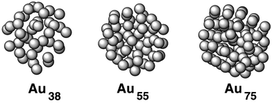 | ||
| Fig. 3 Most stable structures of three gold clusters, with 38, 55 and 75 atoms respectively, obtained from first principles DFT calculations. | ||
Control of the transport properties of molecular conductors through hydrogen bonding
Many of the interesting properties of low-dimensional metals are related to the special topology of their Fermi surface which, in the end, is imposed by the crystal structure. Thus, in order to discuss the origin of these properties and, more importantly, if we want to have some control over them, it is important to be able to understand how the shape of the Fermi surface is related to the crystal structure. This is very important, for instance, in low-dimensional molecular conductors, where there are many examples showing that very slight modifications in the crystal structure can drastically change the conducting properties.The situation is very different from that discussed in the previous section. The conductivity of a molecular metal is largely determined by the electrons near the Fermi level. Thus, in studying the transport properties of molecular metals, we need to focus on the partially filled bands of the system and the corresponding Fermi surface. Consequently, we do not need to use a theoretical approach that correctly describes all the filled levels of the system, i.e. the total energy, but just the partially filled levels. In other words, in understanding the transport properties of a molecular conductor, what we really need is to be able to estimate the interaction between the molecular level that is going to be partially filled (because of the electron transfer) and its nearest neighbours. This is something that is largely dictated by the corresponding overlap integrals, and very simple theoretical approaches, like the tight binding extended Hückel approach, have been of particular value in this area. In order to show how fruitful the collaboration between experimentalists and theoreticians in this field can be, we would like to discuss now a series of salts in which organic radical cations are associated with large all-inorganic anions leading to complex lattice architectures with metallic properties. 30 The goal of this collaboration was to explore some of the strategies that can be used when trying to tune in a rational way the transport properties of low-dimensional molecular conductors.
Let us consider the (BEDT-TTF)
4Re
6Se
5Cl
9·[guest]
{BEDT-TTF = bis(ethylenedithio)tetrathiafulvalene,
guest = DMF, THF, dioxane} series of salts
31
prepared by Batail and co-workers some years ago. The crystal structure
of
m-(BEDT-TTF)
4Re
6Se
5Cl
9·[DMF]
is shown in
Fig. 4, and consists of
layers of BEDT-TTF donors alternating with layers of the [Re
6Se
5Cl
9]
−
cluster. As shown in
Fig. 4, some empty
space remains between the cluster anions. Solvent molecules (not shown
in
Fig. 4 for clarity) occupy these
holes and give cohesion to the structure. It is important to realise that
several of the hydrogen atoms of the BEDT-TTF donor point towards the
solvent position and, thus, the donor layer and the solvent molecules are
related through hydrogen bonds. Hence, the possibility of changing the internal
structure of the donor layers (and, therefore, some of the transfer integrals
of the donor sublattice) by appropriately replacing the solvent molecules
immediately came to mind.

![Crystal structure of
m-(BEDT-TTF)
4Re
6Se
5Cl
9·[DMF]. The DMF guest molecules are
not shown.
31](/image/article/2001/JM/b003683h/b003683h-f4.gif) | ||
| Fig. 4 Crystal structure of m-(BEDT-TTF) 4Re 6Se 5Cl 9·[DMF]. The DMF guest molecules are not shown. 31 | ||
The calculated band structure near the Fermi level for the donor layers of m-(BEDT-TTF) 4Re 6Se 5Cl 9·[DMF] is shown in Fig. 5a. Since the unit cell of the donor layer contains four molecules, there are four bands mainly derived from the BEDT-TTF HOMO (highest occupied molecular orbital). With the average charge required by the stoichiometric formula, i.e. (BEDT-TTF) +1/4, there are seven electrons to fill these bands. As shown in Fig. 5a, the Fermi level associated with this filling intersects the highest of the four bands only, which is, consequently, half-filled. The partially filled band is dispersive along both the a* ( i.e.Γ → X) and c* ( i.e.Γ → Z) directions. However, the dispersion along a* is smaller so that the Fermi level does not intersect the band along this direction, leading to the open Fermi surface shown in Fig. 5b. According to this result, m-(BEDT-TTF) 4Re 6Se 5Cl 9·[DMF] should be a pseudo-1D metal.
![Calculated band structure (a)
and Fermi surface (b) for
m-(BEDT-TTF)
4Re
6Se
5Cl
9·[DMF].
The dashed line in (a) indicates the Fermi level.
Γ,
X,
Z
and
M refer to the wave vectors (0, 0), (
a*/2,
0), (0,
c*/2) and (−
a*/2,
c*/2),
respectively. In (b), the wave vectors of the shaded and unshaded
regions refer to filled and unfilled band levels, respectively.](/image/article/2001/JM/b003683h/b003683h-f5.gif) | ||
| Fig. 5 Calculated band structure (a) and Fermi surface (b) for m-(BEDT-TTF) 4Re 6Se 5Cl 9·[DMF]. The dashed line in (a) indicates the Fermi level. Γ, X, Z and M refer to the wave vectors (0, 0), ( a*/2, 0), (0, c*/2) and (− a*/2, c*/2), respectively. In (b), the wave vectors of the shaded and unshaded regions refer to filled and unfilled band levels, respectively. | ||
Interestingly, at the X point, the dispersion curve shows a minimum which lies very near the Fermi level ( ca. 0.03 eV). A slight perturbation of the lattice affecting the transfer integrals could result in the Fermi level intersecting the band along the a* direction as well and, thus, leading to a closed 2D Fermi surface. Since in this process the X point becomes the locus of a van Hove singularity in the density of states, the physical properties of this type of material could be very exciting to study. The question was: how to induce these perturbations? With the structural information in mind, it was clear that by changing the nature of the guest molecules filling the cavities in between the clusters, slight displacements of the BEDT-TTF molecules would be induced through hydrogen bonding. Thus, for this particular lattice, it was quite apparent that there was the possibility of changing the electronic structure (and thus the transport properties) by using different types of solvent molecules.
Following this reasoning, four different salts of this type were prepared: m-(BEDT-TTF) 4Re 6Se 5Cl 9·[DMF], t-(BEDT-TTF) 4Re 6Se 5Cl 9·[DMF], (BEDT-TTF) 4Re 6Se 5Cl 9·[THF] and (BEDT-TTF) 4Re 6Se 5Cl 9·[dioxane]. 31 Indeed, the internal structure of the donor slabs of these salts showed noticeable differences, although the main architecture was retained. The calculated Fermi surfaces for t-(BEDT-TTF) 4 Re 6Se 5Cl 9·[DMF] and (BEDT-TTF) 4Re 6Se 5Cl 9·[dioxane] are shown in Fig. 6a and b, respectively. While the Fermi surfaces of m-(BEDT-TTF) 4Re 6Se 5Cl 9·[DMF] ( Fig. 5b) and (BEDT-TTF) 4Re 6Se 5Cl 9·[dioxane] ( Fig. 6b) are open, that of t-(BEDT-TTF) 4Re 6Se 5Cl 9·[DMF] ( Fig. 6a) is closed. Thus it is clear that, without disturbing the main architecture of the lattice, just by appropriately changing the nature of the guest molecules, the topology of the Fermi surface can be changed and, thus, the transport properties of the system can be modified.
![Fermi surface calculated
for: (a)
t-(BEDT-TTF)
4Re
6Se
5Cl
9·[DMF]
and (b)
(BEDT-TTF)
4Re
6Se
5Cl
9·[dioxane].
The wave vectors of the shaded and unshaded regions refer to filled and unfilled
band levels, respectively.](/image/article/2001/JM/b003683h/b003683h-f6.gif) | ||
| Fig. 6 Fermi surface calculated for: (a) t-(BEDT-TTF) 4Re 6Se 5Cl 9·[DMF] and (b) (BEDT-TTF) 4Re 6Se 5Cl 9·[dioxane]. The wave vectors of the shaded and unshaded regions refer to filled and unfilled band levels, respectively. | ||
There is another aspect of the strategy outlined above which deserves comment. Depending on the nature and shape of the guest molecule, the size and hydrogen bonding requirements of the cavity can be fulfilled to a different extent. Thus, the guest molecule will have some degree of freedom within the cavity and this can lead to some disorder. For instance, it was the recognition of the inversion disorder of the solvent molecule in (BEDT-TTF) 4Re 6Se 5Cl 9·[THF] that prompted the choice of dioxane as a possible guest molecule in order to reduce such disorder. Indeed, (BEDT-TTF) 4Re 6Se 5Cl 9·[dioxane] has a highly ordered structure. Since it is well known that disorder can have a strong influence on the conductivity of molecular metals, this affords another strategy to slightly change the transport properties of this lattice. It is expected that when the degree of disorder decreases, the probability of electron localisation and, thus, activated conductivity, will also decrease.
The degree of disorder decreases from m-(BEDT-TTF) 4Re 6Se 5Cl 9·[DMF], to (BEDT-TTF) 4Re 6Se 5Cl 9·[THF] and to (BEDT-TTF) 4Re 6Se 5Cl 9·[dioxane], something which is easily understandable in terms of the nature and shape of the different guest molecules. This is nicely reflected in the conductivity of these salts. All of them exhibit high room temperature conductivity and metallic behaviour. When the temperature is decreased, activated behaviour appears in a temperature range that decreases with the amount of disorder in the structure. A broad minimum in the resistivity curve is observed at ca. 90 K for m-(BEDT-TTF) 4Re 6Se 5Cl 9·[DMF], the most severely disordered material. It is shifted down to 50 K for (BEDT-TTF) 4Re 6Se 5Cl 9·[THF] and essentially vanishes in (BEDT-TTF) 4Re 6Se 5Cl 9·[dioxane]. 31 In essence, changing the nature of the guest molecule allowed the suppression of the metal to insulator transition.
There is yet another possibility to modify the transport properties of this type of lattice. As shown by Batail and co-workers, 32 anions with practically the same shape but different charge can be prepared by changing the number of chalcogen and halogen atoms of the cluster. This immediately suggested the possibility of changing the number of electrons filling the HOMO bands of the donor lattice. This possibility has actually been realised and several salts with dianions, like Re 6S 6Cl 82− or Re 6Se 6Cl 82−, have been prepared. 33 The donor lattices of these salts are very similar to those of the monoanions. Consequently, it is expected that the band structures will also be very similar and that the change in the transport properties will only be due to the different filling of the bands.
The calculated band structure and Fermi surface of the (BEDT-TTF) 4Re 6S 6Cl 8·[dioxane] salt are shown in Fig. 7. 34 The band structures of Fig. 7a and 5a are indeed very similar (the band structure of the (BEDT-TTF) 4Re 6Se 5Cl 9·[dioxane] salt, although, of course, not identical, is in fact quite similar to that of Fig. 5a and, thus, it is not shown). Compare, for instance, lines Γ → X and Γ → Z in the two figures (note also that Γ → M in Fig. 5a corresponds to Γ → S in Fig. 7a). However, because of the smaller number of electrons filling these bands, the Fermi level now intersects two bands instead of just one. This leads to a Fermi surface for (BEDT-TTF) 4Re 6S 6Cl 8·[dioxane] ( Fig. 7b) which is very different in shape from that of (BEDT-TTF) 4Re 6Se 5Cl 9·[dioxane] ( Fig. 6b).
![(a) Band
structure and (b) Fermi surface for the donor layers of (BEDT-TTF)
4Re
6S
6Cl
8·[dioxane].
The dashed line in (a) indicates the Fermi level.
Γ,
X,
Z,
M and
S refer to the wave vectors (0, 0), (
a*/2,
0), (0,
c*/2), (
a*/2/,
c*/2)
and (−
a*/2,
c*/2), respectively.](/image/article/2001/JM/b003683h/b003683h-f7.gif) | ||
| Fig. 7 (a) Band structure and (b) Fermi surface for the donor layers of (BEDT-TTF) 4Re 6S 6Cl 8·[dioxane]. The dashed line in (a) indicates the Fermi level. Γ, X, Z, M and S refer to the wave vectors (0, 0), ( a*/2, 0), (0, c*/2), ( a*/2/, c*/2) and (− a*/2, c*/2), respectively. | ||
In agreement with initial expectations, the physical behaviour of the two salts (BEDT-TTF) 4Re 6S 6Cl 8·[dioxane] and (BEDT-TTF) 4Re 6Se 5Cl 9·[dioxane] is very different. Both salts are metals at room temperature, but, while the latter keeps its metallic character down to very low temperatures, the former undergoes an abrupt metal to insulator transition at around 100 K, probably associated with a structural change. This transition can be suppressed under pressure. 34 The Fermi surface of Fig. 7b, which does not exhibit any apparent nesting, does not give hints about the origin of this transition. However, a careful analysis of the different transfer integrals and their geometry dependence suggests that a slight structural change can lead to a modified Fermi surface which is quite well nested by a vector with a c* component of ca. 1/2. 34 This transition would thus be a structurally assisted Peierls distortion, as previously found for (BEDT-TTF) 2ReO 4. 35 In order to test this suggestion, diffuse X-ray scattering studies are needed. Again, the physical properties and Fermi surfaces of the dianion salt can be modified by changing the nature of the guest molecule. For instance, both (BEDT-TTF) 4Re 6Se 6Cl 8·[H 2O] 2 and (BEDT-TTF) 4Re 6S 6Cl 8·[H 2O] 2 are also room temperature metals and have donor lattices very similar to that of (BEDT-TTF) 4Re 6S 6Cl 8·[dioxane], but neither of them exhibits a metal to insulator transition like (BEDT-TTF) 4Re 6S 6Cl 8·[dioxane].
It is clear that this type of salt offers fascinating possibilities for fine tuning of the transport properties. Carefully planned chemical changes can lead to modifications in: (a) the strength of some transfer integrals of the lattice, (b) the electron filling of the bands and (c) the degree of disorder. All of these changes have an important role in controlling the transport properties of this type of lattice but also those of other molecular metals. In recognising many of the ways in which this control can be effectively realised, a close collaboration between experimentalists and theoreticians has been very fruitful.
Understanding the structural modulations and resistivity anomalies of low-dimensional transition metal oxides and bronzes
Low-dimensional transition metal oxides and bronzes with partially filled t 2g bands have been the subject of many studies during the last decade. 13a,36–41 In particular, molybdenum oxides and bronzes have attracted the interest of the solid state community because of the physical properties they exhibit associated with their electronic instabilities. The blue bronzes A 0.3MoO 3 (A = K, Rb, Tl), the purple bronzes A 0.9Mo 6O 17 (A = Li, Na) and AMo 6O 17 (A = K, Tl), as well as the Magnèli phases Mo 4O 11, Mo 8O 23 and Mo 9O 26 have been carefully studied. 13a,36–38 More recently, the large family of monophosphate tungsten bronzes has also received a lot of attention. 39–44 From the structural viewpoint, all these systems are 2D or 3D materials, but several of them behave as if they were 1D or pseudo-1D in terms of their physical behaviour.The electronic instabilities of low-dimensional metals are related to the topology of their Fermi surface. When a piece of a Fermi surface can be translated by a vector q and superimposed on another piece of the Fermi surface, the Fermi surface is said to be nested by the vector q. An example of a perfectly nested Fermi surface is shown in Fig. 8. Metals with nested Fermi surfaces are susceptible towards a modulation with wave vector q of their charge or spin density, which destroys the nested portions of the Fermi surface. Thus, if the nesting is complete, like that in Fig. 8a and b, after the appearance of the modulation the entire Fermi surface is destroyed. The system exhibits a metal to insulator transition. If the nesting is only partial, part of the Fermi surface will remain after the appearance of the modulation and the transition will be of the metal to metal type. Metal to insulator transitions associated with such charge density or spin density waves are frequently observed at low temperature in 1D or pseudo-1D metals. 13 The potassium blue bronze is a typical example of a low-dimensional metal with a completely nested Fermi surface which undergoes a metal to insulator transition associated with a charge density wave. 36,38
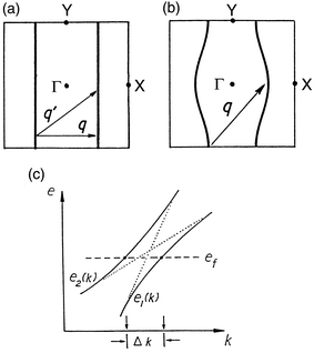 | ||
| Fig. 8 Schematic representation of 1D (a) and a pseudo-1D (b) Fermi surfaces and the associated nesting vectors. (c) Schematic drawing of two band dispersion curves with an avoided crossing near the Fermi level. | ||
Analysis of the Fermi surface nesting requires special consideration for a low-dimensional metal with several partially filled bands. 45Fig. 8c illustrates two band dispersion curves with an avoided crossing in the vicinity of the Fermi level. With an increasing extent of band hybridisation, the separation Δ k between the Fermi vectors becomes larger. In general, such avoided crossings in band dispersion surfaces lead to avoided crossings in the corresponding Fermi surfaces. Therefore, a low-dimensional metal with several partially filled bands may give rise to apparently unnested Fermi surfaces, although their intended surfaces (that is, those expected in the absence of the avoided crossings) are all nested. In such a case, the nesting is hidden by the avoided crossings. Such hidden, nested Fermi surfaces, can lead to charge density waves (CDWs), thereby destroying the nested portions of the combined Fermi surfaces. Thus, to understand the CDW phenomenon of a low-dimensional metal with several partially filled bands, it is essential to search for nesting in the intended, hidden Fermi surfaces.
The potassium purple bronze KMo 6O 17 has separated Mo–O layers of composition Mo 6O 17, which are made up of both MoO 6 octahedra and MoO 4 tetrahedra ( Fig. 9). The sodium and thallium purple bronzes are similar in structure to the potassium purple bronze. The potassium purple bronze is a 2D metal above 120 K, at which temperature it undergoes a CDW phase transition. 38,46–48 It remains 2D metallic after this phase transition. Diffuse X-ray scattering and electron diffraction studies show the occurrence of superlattice spots at a*/2, b*/2 and ( a* − b*)/2 below 120 K. 48 According to the thermoelectric power measurements, the major carriers for electrical transport are electrons and holes above and below 120 K, respectively. Hall effect measurements show that both electrons and holes are present below 120 K. According to these observations, several partially filled d-block bands are present in KMo 6O 17. In electrical, CDW and other physical properties, the sodium and thallium purple bronzes are similar to KMo 6O 17. 47
 | ||
| Fig. 9 (a) Perspective view of two adjacent Mo 6O 17 layers of KMo 6O 17. The c-axis is perpendicular to the layer and the a-axis is perpendicular to the plane of the drawing. (b) Schematic view of the inner Mo 2O 9 layer in KMo 6O 17. | ||
As shown in Fig. 9a, three different types of Mo atoms in AMo 6O 17 exist. 49 According to both electronic band structure calculations 50 and a study of the bond-valence-sum analysis of the metal–oxygen bond lengths, 49 the d electrons of KMo 6O 17 reside primarily in the MoO 6 octahedra of Mo( III). Consequently, the Mo 2O 9 layer formed by the inner two octahedral sublayers plays an important role in determining the electronic structure of KMo 6O 17. The Mo 2O 9 layer is shown schematically in Fig. 9b. A projection view of the Mo 2O 9 layer along the c-axis is given in Fig. 10a.
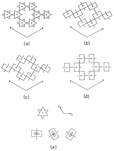 | ||
| Fig. 10 Schematic view of the Mo 2O 9 trigonal layer present in the purple bronze KMo 6O 17. The projection view perpendicular to the layer is shown in (a). The Mo 2O 9 layer is constructed in terms of the Mo 2O 10 zigzag chains running along the a, b and ( a + b) directions in (b), (c) and (d), respectively. Perspective views of the three t 2g-orbitals of an MoO 6 octahedron in the Mo 2O 9 layer are shown in (e), where the d-orbital containing planes are aligned along the a, b and ( a + b) directions of the Mo 2O 9 layer. | ||
KMo 6O 17 has three electrons per unit cell to fill its three lowest-lying d-block bands so that there are three partially filled d-block bands. The Fermi surfaces of the three bands are shown in Fig. 11a–c. 45 These surfaces are all 2D in nature, and their individual partial nesting does not explain the observed CDW vectors. The three surfaces are combined together in Fig. 11d which, upon neglecting the avoided crossings, can be decomposed into three sets of nested 1D surfaces, as illustrated in Fig. 11e. The 1D Fermi surfaces are perpendicular to the a , b and ( a + b) directions of the trigonal lattice.
 | ||
| Fig. 11 Hidden nesting in the purple bronze KMo 6O 17. The calculated Fermi surfaces for the three partially filled d-block bands are shown in (a), (b) and (c), the combined Fermi surfaces in (d), and the hidden 1D Fermi surfaces in (e). | ||
To a first approximation, therefore, the three partially filled bands of KMo 6O 17 are derived from three 1D bands dispersive along the a, b and ( a + b) directions. This conclusion is consistent with the structural and electronic properties of this bronze. As mentioned previously, the conducting electrons are confined to the inner Mo 2O 9 layers (see Fig. 9b and 10a). These layers can be constructed from Mo 2O 10 zigzag chains, running along the a, b or ( a + b) directions, by sharing their axial oxygen atoms, as shown in Fig. 10b–d. The partially filled bands of KMo 6O 17 are made up of the t 2g-orbitals of MoO 6 octahedra. As illustrated in Fig. 10e, the t 2g-orbitals are contained in the planes of the chains (that is, those defined by the equatorial oxygen atoms) running along the a, b and ( a + b) directions. Thus, the t 2g-orbitals are p-orbitals along the intrachain directions, but d-orbitals along the interchain directions. Consequently, the band associated with each of the t 2g-orbitals is dispersive along the associated intrachain direction, but dispersionless along the associated interchain direction. In addition, due to the local orthogonality of the t 2g-orbitals, the three chain bands resulting from the t 2g-orbitals are practically independent of one another, to a first approximation. 13 a,45,50 Thus, for qualitative purposes, the bottom three d-block bands of KMo 6O 17 can be approximated by the three independent 1D bands resulting from the t 2g-orbitals of each octahedra. It is these three ‘hidden 1D bands’ that are responsible for the hidden nesting shown in Fig. 11e. 45
The electronic structure of KMo 6O 17 is essentially represented by the three hidden 1D bands. Since there are three electrons to fill these bands, each band is half-filled. Consequently, the t 2g-block bands of KMo 6O 17 can be viewed as a superposition of three almost independent half-filled 1D bands. It is this observation that led to the formulation of the concept of hidden nesting. 45
A CDW formation introduces an additional periodicity of electron density distribution into the lattice and, hence, gives rise to superlattice reflections in the X-ray or electron diffraction pattern below the CDW phase transition temperature Tp. At temperatures above Tp, a nested 1D Fermi surface leads to CDW fluctuations. The latter cause planar diffuse scattering and, hence, 2 kf diffuse lines between layers of main Bragg reflections in X-ray diffraction patterns. 48,51 Thus, like any 1D metallic system with CDW instability, KMo 6O 17 was predicted 45 to show 1D CDW fluctuations above 120 K and, hence, diffuse lines in the X-ray patterns. As schematically shown in Fig. 12, the diffuse lines resulting from the CDW fluctuations of the chains along the a, b or ( a + b) directions should be perpendicular to the chain direction and are located at the midpoints between the rows of the main Bragg spots perpendicular to the chain direction. Thus, the three sets of the diffuse lines should form hexagons around each main Bragg reflection spot ( Fig. 12).
 | ||
| Fig. 12 Schematic representation of the X-ray pattern in the ( a*, b*) plane above 120 K expected from the hidden nesting of KMo 6O 17. The heavy dots refer to Bragg reflections. | ||
The pattern of diffuse lines predicted by Fig. 12 was observed by diffuse X-ray scattering experiments on AMo 6O 17 (A = K, Na) at room temperature. 45 As the temperature is lowered below 120 K, the diffuse lines in Fig. 12 condense into satellite reflections at a*/2, b*/2 and ( a* − b*)/2, which are the cross-section points of the diffuse lines. The nesting in the real Fermi surfaces ( Fig. 11d) is not as complete as in the hidden surfaces ( Fig. 11e), so that some small pieces of the Fermi surface (for example, small electron and hole pockets) may remain (especially in the avoided crossing regions) after the CDW phase transition. This would explain the semimetallic properties of AMo 6O 17 observed below 120 K by galvanometric measurements. 38,46 Angle-resolved photoemission experiments on the sodium purple bronze also confirmed the occurrence of hidden nesting in these bronzes. 52,53
The concept of hidden nesting was soon found to be essential in explaining the resistivity anomalies of a number of oxides and bronzes, like the Magnéli phases γ- and η-Mo 4O 1154 and the family of monophosphate tungsten bronzes (PO 2) 4(WO 3) p(WO 3) q ( p and q are integer numbers related to the width of the octahedral layers). 44 These solids also contain metal–oxygen layers made up of MO 6 octahedra and possess partially filled t 2g-block bands. As for the purple bronzes, the three t 2g-block orbitals of each MO 6 octahedron are contained in three mutually orthogonal planes, and act as δ-orbitals toward the M–O axes perpendicular to these planes. Consequently, as a first approximation, these metal–oxygen layers can be regarded as made up of three noninteracting sets of t 2g-orbital containing chains, as far as their t 2g-block bands are concerned. The interest of the Magnéli phases and the monophosphate tungsten bronzes is that the three t 2g-orbital containing chains are not equivalent. 43 This leads to interesting new features in the low temperature behaviour of these solids that have recently received a lot of attention. 36,39–43 Again, the understanding of the puzzling behaviour of these low-dimensional materials through the development of the hidden nesting concept was only possible because of close collaboration between theoreticians and experimentalists.
Absorption of atoms and molecules and growth of thin films on silicon surfaces
The field of deposition on surfaces is of great importance, especially in the case of silicon: most of the devices used in microelectronics are obtained by surface-related processes on the silicon substrate. Therefore, the possibility of growing new materials on silicon can open routes to applications in microelectronics devices, which makes the field of deposition and growth on silicon a very active one. Here theory has also contributed a large amount, together with experiment. We will discuss a few cases here as an illustration.In recent years, it has become possible to grow epitaxial thin films of perovskite oxides on silicon. The importance of this is enormous: these oxides present a range of properties like ferroelectricity, high dielectric constant, high temperature superconductivity and giant magnetoresistance, to mention just a few. Thin films of SrTiO 3 (a material of high dielectric constant) and BaTiO 3 (a ferroelectric material) were recently 55 grown epitaxially on Si(001), opening the possibility for their use in integrated circuits, for instance as gate oxides for field effect transistors, or as storage media for non-volatile memories. The growth process is complicated and it seems that an essential step is the deposition of a sub-monolayer of Sr or Ba to avoid interdiffusion. Wang and co-workers 56 have studied the first stages of Ba deposition on a clean Si(001) surface, to understand the microscopic details of the growth process from its initial stages. The theoretical results are complemented by experimental STM images, which give an idea of the most likely positions of the Ba atoms, and the evolution with Ba concentration of the surface. The theoretical calculations in the limit of low Ba concentration show that the most favourable site of absorption is the trench between rows of silicon dimers (site A in Fig. 13). This is in contrast with the situation found in other alkali and alkaline earth metals on silicon, where other sites (like the middle of a dimer, or the position between dimers) are the most stable. In the case of Ba (and also Sr), the large size of the metal atoms makes it possible to form four bonds with the four silicon atoms located at the dimer rows adjacent to site A, and this makes the site a very stable one (since the Ba atom bonds to the dangling bonds of the Si atoms). Site B is also relatively stable, but 0.8 eV higher in energy than A (since the bond is not directed towards the dangling bonds of the Si atoms). An analysis of the Mulliken populations and the transfer of charge at the A site shows that, despite the large difference in electronegativity between Si and Ba, which would suggest an ionic bond, the charge transfer is rather small (only 0.15 e). There is, however, a large redistribution of charge in the close surroundings of the Ba atom (from the 6s-orbitals to the 6p and 5d-orbitals). This suggests the formation of a covalent bond between the Ba atom and the surface, and explains the core-level shift experiments of Cheng and co-workers, 57 who found a small or zero charge transfer at low coverage, in contrast to the ionic character of the metal silicides obtained at high coverage (above 1 monolayer). The results of the calculation are also consistent with the STM experiments 58 which also indicate a small charge transfer from Ba to Si in the low coverage regime.
 | ||
| Fig. 13 Surface potential energy map (in eV) of a Ba atom on a Si(001) surface, from first principles DFT calculations. A sketch of the dimer rows in the (2 × 1) reconstruction is shown as a reference to the energy map. | ||
An interesting issue that remains to be solved is the observation of absorption sites by STM 58 which are not consistent with the theoretical results of the absorption energy presented above. Although most of the experimentally observed absorption sites correspond to the theoretically predicted minimum energy configuration (site A), some Ba atoms are absorbed above the mid-point of a Si–Si dimer. This corresponds to an energy maximum, according to the calculations, and therefore should be a very unlikely absorption site. Work in progress by Tobías and Ordejón 59 explains this contradictory result by suggesting that the Ba atoms observed at these sites are not on top of a dimer, but on a missing-dimer defect site. Since the Ba is a large atom, the STM image can not determine if the dimer is present or missing, so the experiment alone can not define the situation. The calculations indicate that the absorption of a Ba atom on top of a missing dimer is very favourable energetically (even more stable than the site A absorption), and therefore we should expect to observe some Ba atoms in these sites, which often occur on clean Si(001) surfaces.
A last illustration of the interplay between theory and experiment in surface
problems is the recent observation of molecular orbital (MO) features
in C
60 fullerene molecules absorbed on Si(111) surfaces.
60 MOs represent such a cornerstone in our understanding
of molecular bonding and structure that drawings of them can be found in any
quantum chemistry book. However, direct experimental visualization has proven
very difficult because of technical and conceptual problems (energy resolution,
interaction with the substrate,
etc). Recently, Pascual and
co-workers
60 have reported the observation
of clear MOs of C
60 by means of STM imaging. The molecules were
deposited on a Si(111)
(7 × 7) surface,
in which the fullerenes are firmly anchored (because of the dangling
bonds in the clean surface, which bond to the C atoms of the fullerene).
In the STM images, molecules with two different apparent sizes can be observed.
Upon annealing at 600![[thin space (1/6-em)]](https://www.rsc.org/images/entities/char_2009.gif) °C, the ‘large’ molecules evolve
into ‘small’ ones, indicating that the last case corresponds to
a more stable absorbed configuration. For this configuration, a rich variety
of internal structures can be observed in the experimental STM images.
Fig. 14a–d shows some of the most characteristic
shapes, which are reproducible under different experimental conditions. The
molecules in
Fig. 14a–c give
evidence of the expected decrease of the icosahedral symmetry after interaction
with the surface, since each one appears with an intramolecular pattern resembling
the 3, 2 and 5-fold rotational symmetry of the free molecules, respectively.
°C, the ‘large’ molecules evolve
into ‘small’ ones, indicating that the last case corresponds to
a more stable absorbed configuration. For this configuration, a rich variety
of internal structures can be observed in the experimental STM images.
Fig. 14a–d shows some of the most characteristic
shapes, which are reproducible under different experimental conditions. The
molecules in
Fig. 14a–c give
evidence of the expected decrease of the icosahedral symmetry after interaction
with the surface, since each one appears with an intramolecular pattern resembling
the 3, 2 and 5-fold rotational symmetry of the free molecules, respectively.
 | ||
| Fig. 14 Comparison of the experimental STM images of individual C 60 molecules on Si(111) (a–d) with the calculated molecular orbitals of the free molecule (e–h). In the calculation, a uniaxial deformation of 5% was applied along an axis of three- (e), two- (f), five- (g) and threefold symmetry (h). In (e–g), the axis was perpendicular to the plotting plane, whereas (h) was rotated an angle of 30°. In all cases, the orbitals plotted are the HOMO. | ||
The interpretation and explanation of the observed images is greatly facilitated by theoretical calculations. A detailed theoretical calculation of a STM image is a difficult and demanding task, since the interaction of the substrate, molecule and tip must be included. However, the clear intramolecular features of the observed C 60 images suggest that some information can be extracted from a calculation of the MOs of the isolated molecule, as a first approximation to the experimental setup. To break the energy level degeneracies, and simulate the observed decrease of the molecular symmetry induced by the substrate, we applied a small strain along different molecular axes in the calculations. In doing so, we found that the experimental patterns are reproduced in great detail in the calculated shape of the new HOMO of this free but compressed molecule ( Fig. 14e–g). Note that the HOMO level is the one that is expected to contribute to the STM current, and therefore its shape will be sampled in the STM image. Other combinations of MOs other than the HOMO give a substantially poorer comparison with the experimental images. The close agreement between theory and experiment reveals that only one of the MOs arising from the initially quintuply degenerate HOMO is mainly responsible for electron transport through the molecule. We note that, despite the strong interaction between molecule and surface, it is possible to find experimental systems where a simple analysis in terms of MOs is justified, and highlights again the importance of the interplay between theory and experiment in extracting relevant physical and chemical information on the behaviour of solid state systems.
Concluding remarks
The development in recent years of very powerful DFT techniques has made it possible to perform reliable atomistic simulations of very complex materials. Almost simultaneously, a conceptual framework merging the approaches of solid state physicists and molecular chemists in order to understand the structure and properties of inorganic solids has also been put forward. As we have tried to make clear through the discussion of a few selected examples, these two developments now make possible a real and fruitful interaction between experimentalists and theoreticians on most aspects of contemporary solid state inorganic chemistry.Acknowledgements
The problems discussed in this work have been studied in close collaboration with several experimental and theoretical groups. We would like to thank the groups of P. Batail (Nantes), J.-P. Pouget (Orsay), M.-H. Whangbo (Raleigh), R. Martin (Illinois) and A. Baró (Madrid) for continuing and very fruitful collaborations. This work was supported by DGES-Spain (Project PB96-0859), Generalitat de Catalunya (1997 SGR 24) and Fundación Ramón Areces (Spain). P. O. acknowledges support from Motorola PSRL, Phoenix, AZ (USA). Part of the computations described in this work were carried out using the resources of CESCA and CEPBA coordinated by C 4.References
- P. Hohenberg and W. Kohn, Phys. Rev., 1964, 135, 864 Search PubMed.
- W. Kohn and L. J. Sham, Phys. Rev., 1965, 140, 1133 Search PubMed.
- R. Car and M. Parrinello, Phys. Rev. Lett., 1985, 55, 2471 CrossRef CAS.
- M. C. Payne, M. P. Teter, D. C. Allan, T. A. Arias and J. D. Joannopoulos, Rev. Mod. Phys., 1992, 64, 1045 CrossRef CAS.
- For reviews, see: (a) P. Ordejón, Comput. Mater. Sci., 1998, 12, 157 CrossRef CAS; (b) S. Goedecker, Rev. Mod. Phys., 1999, 71, 1085 CrossRef CAS.
- For reviews, see: (a) W. E. Pickett, Comput. Phys. Rep., 1989, 9, 115 Search PubMed; (b) D. J. Singh, Planewaves, Pseudopotentials and the LAPW Method, Kluwer, Dordrecht, 1994 Search PubMed; (c) M. Fuchs and M. Scheffler, Comput. Phys. Commun., 1999, 119, 67 CrossRef CAS.
- M. Parrinello, Solid State Commun., 1997, 102, 107 CrossRef.
- (a) P. Ordejón, E. Artacho and J. M. Soler, Phys. Rev. B, 1996, 53, R10441 CrossRef CAS; (b) D. Sánchez-Portal, P. Ordejón, E. Artacho and J. M. Soler, Int. J. Quantum Chem., 1997, 65, 453 CrossRef; (c) E. Artacho, D. Sánchez-Portal, P. Ordejón, A. García and J. M. Soler, Phys. Status Solidi B, 1999, 215, 809 CrossRef CAS; (d) P. Ordejón, Phys. Status Solidi B, 2000, 217, 335 CrossRef CAS.
- P. E. Blöchl, Phys. Rev. B, 1994, 50, 17953 CrossRef.
- M. Bockstedte, A. Kley, J. Neugebauer and M. Scheffler, Comput. Phys. Commun., 1997, 107, 187 CrossRef CAS.
- (a) R. Hoffmann, Solids and Surfaces, VCH, New York, 1988 Search PubMed; (b) R. Hoffmann, Angew. Chem., Int. Ed. Engl., 1987, 26, 846 CrossRef; (c) R. Hoffmann, Rev. Mod. Phys., 1988, 60, 601 CrossRef CAS.
- (a) J. K. Burdett, Chemical Bonding in Solids, Oxford University Press, New York, 1995 Search PubMed; (b) J. K. Burdett, Prog. Solid State Chem., 1984, 15, 173 CrossRef CAS.
- (a) E. Canadell and M.-H. Whangbo, Chem. Rev., 1991, 91, 965 CrossRef CAS; (b) M. H. Whangbo, in Crystal Chemistry and Properties of Materials with Quasi-One-Dimensional Structures, ed. J. Rouxel, Reidel, Dordrecht, 1986, p. 27. Search PubMed.
- (a) M.-H. Whangbo and R. Hoffmann, J. Am. Chem. Soc., 1978, 100, 6093 CrossRef CAS; (b) a modified Wolfsberg–Helmholtz formula was used to calculate the non-diagonal H ij matrix elements ( J. Ammeter, H.-B. Bürgi, J. Thibeault and R. Hoffmann, J. Am. Chem. Soc., 1978, 100, 3686). Search PubMed.
- (a) N. Agraït, G. Rubio and S. Vieira, Phys. Rev. Lett., 1995, 74, 3995 CrossRef; (b) J. I. Pascual, J. Méndez, J. Gómez-Herrero, A. M. Baró, N. García, U. Landman, W. D. Luedtke, E. N. Bogachek and H. P. Cheng, Science, 1995, 267, 1793 CAS.
- (a) C. J. Muller, J. M.. van Ruitenbeek and L. J. de Jongh, Phys. Rev. Lett., 1992, 69, 140 CrossRef CAS; (b) J. M. Krans, J. M. van Ruitenbeck, V. V. Fisun, I. K. Janson and L. J. de Jongh, Nature, 1995, 375, 767 CrossRef CAS; (c) N. Agraït, J. C. Cuevas, A. L. Yeyati, B. Ludolph, A. Martín-Rodero, G. Rubio Bollinger, J. van Ruitenbeek, C. Urbina and E. Scheer, Nature, 1998, 394, 154 CrossRef.
- J. L. Costa-Krämer, N. García, P. García-Mochales and P. A. Serena, Surf. Sci., 1995, 342, L1144 CrossRef.
- (a) H. Ohnishi, Y. Kondo and K. Takayanagi, Nature, 1998, 395, 780 CrossRef CAS; (b) A. I. Yanson, G. Rubio Bollinger, H. E. van den Brom, N. Agraït and J. M. van Ruitenbeek, Nature, 1998, 395, 783 CrossRef CAS.
- Y. Kondo and K. Takayanagi, Bull. Am. Phys. Soc., 1999, 44, 312 Search PubMed.
- A. Torres, E. Tosatti, A. dal Corso, F. Ercolessi, J. J. Kohanoff, F. Di Tolla and J. M. Soler, Surf. Sci. Lett., 1999, 426, L441 Search PubMed.
- D. Sánchez-Portal, J. Junquera, P. Ordejón, A. García, E. Artacho and J. M. Soler, Phys. Rev. Lett., 1999, 83, 3884 CrossRef CAS.
- See, for instance: (a) R. L. Whetten, J. T. Khoury, M. M. Alvarez, S. Murthy, I. Vezmar, Z. L. Wang, P. W. Stephens, C. L. Cleveland, W. D. Luedtke and U. Landman, Adv. Mater., 1996, 5, 8.
- W. D. Luedtke and U. Landman, J. Phys. Chem., 1996, 100, 13323 CrossRef CAS.
- C. L. Cleveland, U. Landman, T. G. Schaaff, M. N. Shafigullin, P. W. Stephens and R. L. Whetten, Phys. Rev. Lett., 1997, 79, 1873 CrossRef CAS.
- J. A. Ascencio, C. Gutierrez-Wing, M. E. Espinosa, M. Marín, S. Tehuacanero, C. Zorrilla and M. J. Yacamán, Surf. Sci., 1998, 396, 349 CrossRef CAS.
- I. L. Garzón and A. Posada-Amarillas, Phys. Rev. B, 1996, 54, 11796 CrossRef CAS.
- I. L. Garzón, K. Michaelian, M. R. Beltrán, A. Posada-Amarillas, P. Ordejón, E. Artacho, D. Sánchez-Portal and J. M. Soler, Phys. Rev. Lett., 1998, 81, 1600 CrossRef CAS.
- J. M. Soler, M. Beltrán, K. Michaelian, I. L. Garzón, P. Ordejón, D. Sánchez-Portal and E. Artacho, Phys. Rev. B, 2000, 61, 5771 CrossRef CAS.
- K. Michaelian, Chem. Phys. Lett., 1998, 293, 202 CrossRef CAS.
- For recent reviews see: (a) C. J. Kepert, M. Kurmoo and P. Day, Proc. R. Soc. London, Ser. A, 1998, 454, 487 Search PubMed; (b) E. Coronado and C. Gómez-García, Chem. Rev., 1998, 98, 273 CrossRef CAS.
- A. Pénicaud, K. Boubekeur, P. Batail, E. Canadell, P. Auban-Senzier and D. Jérome, J. Am. Chem. Soc., 1993, 115, 4101 CrossRef CAS.
- S. Uriel, K. Boubekeur, P. Batail, J. Orduna and E. Canadell, Inorg. Chem., 1995, 34, 5307 CrossRef CAS.
- (a) P. Batail, K. Boubekeur and A. Deluzet, unpublished results ; (b) C. Guilbaut, PhD Thèse, Université de Nantes, 1999; (c) A. Deluzet, PhD Thèse, Université de Nantes, 2000. .
- P. Batail, K. Boubekeur, C. Guilbaud, A. Deluzet, C. Pasquier, P. Auban-Senzier, D. Jérome, R. Rousseau and E. Canadell, unpublished results. .
- M.-H. Whangbo, J. Ren, W. Liang, E. Canadell, J. P. Pouget, S. Ravy, J. M. Williams and M. A. Beno, Inorg. Chem., 1992, 31, 4169 CrossRef CAS.
- (a) Low-Dimensional Electronic Properties of Molybdenum Bronzes and Oxides, ed. C. Schlenker, Kluwer, Dordrecht, 1989 Search PubMed; (b) Physics and Chemistry of Low-Dimensional Inorganic Conductors, ed. M. Greenblatt, C. Schlenker, J. Dumas and S. van Smaalen, NATO ASI Ser., Ser. B, Plenum, New York, 1996. Search PubMed.
- (a) M. Greenblatt, Chem. Rev., 1988, 88, 31 CrossRef CAS; (b) C. Schlenker, J. Dumas, C. Escribe-Filippini, H. Guyot, J. Marcus and J. Fourcadot, Philos. Mag. B, 1985, 52, 643 Search PubMed.
- J. Dumas and C. Schlenker, Int. J. Mod. Phys. B, 1993, 7, 4045 CrossRef CAS.
- M. Greenblatt, Int. J. Mod. Phys. B, 1993, 7, 3937 CrossRef CAS.
- (a) P. Foury and J. P. Pouget, Int. J. Mod. Phys. B, 1993, 7, 3973 CrossRef CAS; (b) A. Ottolenghi and J. P. Pouget, J. Phys. I, 1996, 6, 1059 Search PubMed.
- (a) C. Schlenker, C. Hess, C. Le Touze and J. Dumas, J. Phys. I, 1996, 6, 2061 Search PubMed; (b) J. Dumas, C. Hess, C. Schlenker, G. Bonfait, E. Gomez Marín, D. Groult and J. Marcus, Eur. Phys. J. B, 2000, 8, 9923.
- (a) E. Canadell and M.-H. Whangbo, Phys. Rev. B, 1991, 43, 1894 CrossRef CAS; (b) E. Wang, M. Greenblatt, I. E.-I. Rachidi, E. Canadell, M.-H. Whangbo and S. Vadlamannati, Phys. Rev. B, 1989, 39, 12969 CrossRef CAS.
- E. Canadell and M.-H. Whangbo, Int. J. Mod. Phys. B, 1993, 7, 4005 CrossRef CAS.
- B. Raveau, Proc. Indian Nat. Sci. Acad., 1986, A52, 67 Search PubMed.
- M.-H. Whangbo, E. Canadell, P. Foury and J. P. Pouget, Science, 1991, 252, 96 CAS.
- C. Schlenker, J. Dumas, C. Escribe-Filippini and H. Guyot, in Low-Dimensional Electronic Properties of Molybdenum Bronzes and Oxides, ed. C. Schlenker, Kluwer, Dordrecht, 1989, p. 159. Search PubMed.
- M. Greenblatt, in Low-Dimensional Electronic Properties of Molybdenum Bronzes and Oxides, ed. C. Schlenker, Kluwer, Dordrecht, 1989, p. 1. Search PubMed.
- J. P. Pouget, in Low-Dimensional Electronic Properties of Molybdenum Bronzes and Oxides, ed. C. Schlenker, Kluwer, Dordrecht, 1989, p. 87. Search PubMed.
- H. Vincent, M. Ghedira, J. Marcus, J. Mercier and C. Schlenker, J. Solid State Chem., 1987, 47, 113 CrossRef CAS.
- M.-H. Whangbo, E. Canadell and C. Schlenker, J. Am. Chem. Soc., 1987, 109, 6308 CrossRef CAS.
- R. Moret and J. P. Pouget, in Crystal Chemistry and Properties of Materials with Quasi-One-Dimensional Structures, ed. J. Rouxel, Reidel, Dordrecht, 1986, p. 87. Search PubMed.
- K. Breuer, C. Stagarescu, K. E. Smith, M. Greenblatt and K. Ramanujachary, Phys. Rev. Lett., 1996, 76, 3172 CrossRef CAS.
- G.-H. Gweon, J. W. Allen, R. Claessen, J. A. Clack, D. M. Poirier, P. J. Benning, G. C. Olson, W. P. Ellis, Y.-X. Zhang, L. F. Schneemeyer, J. Marcus and C. Schlenker, J. Phys.: Condens. Matter, 1996, 8, 9923 Search PubMed.
- (a) M. Ghedira, H. Vincent, M. Marezio, J. Marcus and G. Fourcadot, J. Solid State Chem., 1985, 56, 66 CAS; (b) L. Kihlborg, Ark. Kemi, 1963, 21, 365 Search PubMed; (c) A. Magnéli, Acta Chem. Scand., 1948, 2, 861 Search PubMed.
- R. A. McKee, F. J. Walker and M. F. Chisholm, Phys. Rev. Lett., 1998, 81, 3014 CrossRef CAS.
- J. Wang, J. Hallmark, D. S. Marshall, W. J. Ooms, P. Ordejón, J. Junquera, D. Sánchez-Portal, E. Artacho and J. M. Soler, Phys. Rev. B, 1999, 60, 4968 CrossRef CAS.
- C.-P. Cheng, I.-H. Hong and T.-W. Pi, Phys. Rev. B, 1998, 58, 4066 CrossRef CAS.
- X. Yao, X. Hu, D. Sarid, Z. Yu, J. Wang, D. S. Marshall, R. Droopad, J. K. Abrokwah, J. A. Hallmark and W. J. Ooms, Phys. Rev. B, 1999, 59, 5115 CrossRef CAS.
- G. Tobías and P. Ordejón, unpublished results. .
- J. I. Pascual, J. Gómez-Herrero, C. Rogero, A. M. Baró, D. Sánchez-Portal, E. Artacho, P. Ordejón and J. M. Soler, Chem. Phys. Lett., 2000, 231, 78 CrossRef.
Footnote |
| † Basis of a presentation given at Materials Discussion No. 3, 26–29 September, 2000, University of Cambridge, UK. |
| This journal is © The Royal Society of Chemistry 2001 |