Ultrapure water quality monitoring by a silicon-based potentiometric sensor
Oliver Chyan*a, Jin-Jian Chena, Fei Xua, Jennifer A. Seesb and Lindsey H. Hallb
aDepartment of Chemistry, University of North Texas, Denton, TX 76203., USA
bTexas Instruments, Dallas, TX 752, USA
First published on UnassignedUnassigned7th January 2000
Abstract
A solid state silicon-based potentiometric sensor and a resistivity sensor were employed to monitor the water quality from an ultra-pure water production unit. A minute ionic impurity increase (at the low ppt level), which was not detectable by the conventional water resistivity sensor, can be sensitively detected by the silicon-based sensor. This slight degradation of water purity, independently confirmed by inductively coupled plasma mass spectrometry and atomic force microscopy, was attributed to early boil-off from the saturated water purification cartridge. The silicon-based sensor can potentially function as an ultra-sensitive monitoring sensor in conjunction with the conventional resistivity sensor to ensure water purity at parts per trillion level.
Introduction
High-purity water is an essential chemical used by many ‘high-tech’ industries including the pharmaceutical, biogenetic, and microelectronics industries. Stringent water purity control is especially important for the silicon-based microelectronics sector, which on average requires more than 2000 gallons of ultra-pure water to process a single silicon wafer.1 To assure optimal integrated circuit fabrication yield, the production of ultra-pure water is carefully monitored to maintain impurities at or below the one part per trillion level. Routine water purity monitoring is commonly carried out off-line using inductively coupled plasma mass spectrometry (ICP-MS). Alternatively, water resistivity measurements also afford an on-line, low cost, but less sensitive (vide infra) means of water purity monitoring.Recently, we reported a new class of silicon-based sensor which provides a sensitive detection of parts per billion (ppb) to parts per trillion (ppt) ionic impurities in high-purity hydrofluoric acid (HF) and alkaline hydrogen peroxide solution (NH4OH–H2O2–H2O). 2,3 In HF solution, trace levels of metal ion impurities such as Ag+, Cu2+, Au3+, Pt2+ and Pd2+ can readily be reduced and deposited as zero-valence metal nanoparticles on an oxide-free silicon surface.4 The nanoscale metal deposition acts to extract surface electrons from the silicon electrode surface and to shift the silicon open-circuit potential to more positive values to achieve below ppb detection sensitivity. The ultrasensitive detection capability makes the sensor useful in on-line monitoring of the metal contamination onset and assuring the chemical purity at the point of use for the microelectronics fabrication process.
In this work, we applied the silicon-based sensor to monitor the complete life cycle of a purification cartridge in an ultra-pure water purification unit. The water purity was also independently determined by a resistivity sensor and by ICP-MS. Our silicon-based sensor detected a minute increase of ionic impurity which was independently confirmed by ICP-MS to be at the low ppt level. The premature boil-off from the saturated purification cartridge after 80 d of continuous operation caused a slight degradation of water purity. The silicon-based sensor can potentially function as an ultra-sensitive (at ppt levels) impurity monitoring sensor to complement the conventional water resistivity sensor (sensitive to ppb levels) in assuring the water purity down to a low ppt level.
Experimental
The ultra-pure water (UPW) purification system (Millipore) consists of a pre-treatment pack, a reverse osmosis unit and a final polishing module. The pre-treatment pack removed contaminants and softened the tap feed water. The reverse osmosis unit removed all types of contaminants (particles, pyrogens, micro-organisms, colloids and dissolved inorganics) to different extents (90–99%). The final polishing module combined with ultraviolet radiation (254 nm) further purified the reverse osmosis pre-treated water by removing trace levels of any residual contaminants. The UPW as-prepared above was analyzed by ICP-MS (Fisons, Model PQS) which measured 36 elements, relevant to semiconductor applications, to be below the instrument detection limit (<1 ppt).The UPW quality was concurrently analyzed using the silicon-based potentiometric sensor.2,3 The silicon sensing electrodes were prepared from prime Si(111) wafers (Wacker, boron-doped, 0.01–0.02 Ω cm). The silicon chips (1 × 1 cm) were first cleaned in the standard silicon wafer cleaning solutions (HF, NH4OH–H2O2, HCl–H2O2). Prior to placing in the sensor holder, the silicon sensor chip was freshly etched by HF solution (0.49%, Hashimoto, ultra-pure grade) followed by ultra-pure water rinsing. A custom-made perfluoroalkoxy polymer (PFA) sensor holder with double O-ring seals, as illustrated in Fig. 1, was used to isolate the solution contact only to the front polished surface of the silicon sensor chip. The viton O-rings were encapsulated by Teflon to minimize potential contamination from the O-rings through acid leaching. The electrical contact was made to the back side of the silicon chip using Ga/In eutectic (99.99%, AESAR).
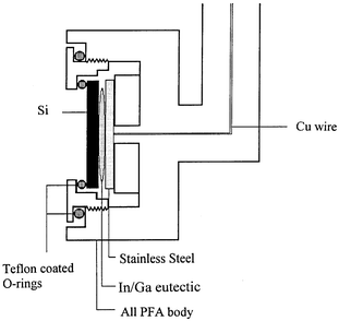 | ||
| Fig. 1 Custom-made perfluoroalkoxy polymer sensor holder to isolate the solution contact only to the front polished surface of the silicon sensor chip. | ||
The open-circuit potential of the silicon-based sensor submerged in the non-stirred UPW sample which was exposed to a class one clean room atmosphere was measured with respect to a double-junction reference electrode (Ag–AgCl, Orion) using a high input impedance potentiometer (Accumet 50, Fisher Scientific). Dilute acid electrolyte (0.01% HF, Hashimoto, ultra-pure grade) was added to the UPW sample to increase the electrical conductivity. The outer junction solution (10% KNO3) was replaced after each potential measurement to ensure that there was no detectable contamination originating from the reference electrode. The average silicon sensor potential based on five duplicate measurements was reported. An atomic force microscope (Digital Nanoscope III) was used to image the silicon sensing electrode surface before and after the potentiometric measurement. Preceding each experiment, all the Teflon labware including the PFA sensor holder was cleaned by boiling three times in 10% HNO3 for 30 min followed by thorough rinsing with ultra-pure water.
Results
Fig. 2 shows the time-dependent open-circuit potential responses from two silicon-based sensing electrodes immersed in UPW samples. Water sample (a) was collected 12 d after the installation of a new purification cartridge. Water sample (b) was collected after the purification cartridge had undergone more than 4 months of continuous operation in the UPW system. The purification cartridge treated an estimated volume of 2500 gallons of water during this time period. As shown in Fig. 2, the open-circuit potential reading from the silicon sensor increased by an average of 26 ± 3 mV after 130 d of continuous operation. | ||
| Fig. 2 Time-dependent silicon sensor potential responses from two water samples prepared in 0.01% HF. Sample (a) was collected at 12 d after the installation of a new purification filter. Sample (b) was collected after 130 d. | ||
The surface morphology of the silicon sensing electrode after the aforementioned potentiometric measurements was examined using a high resolution atomic force microscope. The imaging data indicate that submerging in the water sample (a) has no observable effects on the silicon sensing surface morphology, which remains clean and featureless [Fig. 3(a)]. In contrast, segregated nanometer-sized deposits were clearly visible on the silicon sensor surface [Fig. 3(b)] after immersing in the less pure water sample (b) as indicated by the higher silicon potential reading in Fig. 1.
 | ||
| Fig. 3 Atomic force microscopy reveals different surface morphologies (3 × 3 μm, Z = 10 nm) observed from the silicon sensing electrodes after the potentiometric measurements in Fig. 2(a) and (b) (see text for details). | ||
For the comparative study, both the resistivity and silicon-based sensors were used simultaneously to monitor the water quality, throughout the entire life cycle of the purification cartridge in the UPW production unit. Fig. 4 illustrates the water monitoring results obtained in a period of 150 d. The resistivity cell readings were found to remain at a constant level of 18.2 MΩ cm (i.e., the maximum resistivity readout) throughout the monitoring period. In contrast, the silicon-based sensor revealed a persistent and significant potential increase (ca. 25 mV) with respect to the baseline potential after 80 d of water production. The silicon-sensor potential reading was found to return to its initial baseline level (−367 ± 3 mV) after the installation of a new filtration cartridge
 | ||
| Fig. 4 Operation life cycle of a purification cartridge monitored by both the silicon-based and resistivity sensors. | ||
Concurrently, the water samples were independently analyzed by ICP-MS. Fig. 5 depicts the observed changes in the ionic impurity levels based on ICP-MS measurements performed with water samples collected on the 12th and 130th day. According to the ICP-MS data, the water sample (a) collected on the 12th day is very pure with all 36 measured ionic impurities at or below the instrument detection limit (⩽1 ppt). Following continuous operation for 130 d, (see Fig. 5), slightly higher levels of 12 ionic impurities (below 50 ppt) were found to leak through the aged purification cartridge.
 | ||
| Fig. 5 ICP-MS data indicate that water sample (a) is ultrapure (B.D.L. = below detection limit) and sample (b) has a higher level of ionic impurities. | ||
Discussion
The open-circuit potential of the silicon-based sensing electrode is extremely sensitive to trace levels of metal ion impurities in HF solutions.2,3 For example, the detection sensitivity of the silicon sensing electrode towards Ag+ in dilute HF solution is ca. 150 mV per decade change of [Ag+], which is more than twice that of the common electrochemical sensor based on the Nernstian equilibrium (59 mV per decade concentration change). However, the operation mechanism that contributes to the silicon-based sensor’s sensitive response is not straightforward due to the complex surface reactions that take place at the silicon/solution interface. For instance, the proton exchange reaction originating from silicon surface hydrides should play an important role in establishing a stable silicon potential in pure HF solution.5 With the addition of metal ion impurities, nanometer-sized deposits were consistently observed on the silicon surface by atomic force mciroscopy. The nanometer-sized deposits on the silicon surface are mainly zero-valence metal particles as previously identified by TEM and XPS.6,7 Our surface infrared absorption results (not shown in this work) indicate that the silicon sensor surface after discrete metal deposition is still largely terminated by surface hydrides. Consequently, different electron transfer processes can be established between solution species and different regions of the silicon surface. The proton exchange reaction should still be in effect at the silicon hydride region not covered by metal particles. Other surface reactions such as metal deposition by electron extraction from valence band,8 formation of microscopic metal/silicon Schottky barrier junctions,9 metal-induced silicon surface corrosion and other electron transfer processes could all contribute to the final stable silicon potential. Therefore, the observed steady-state silicon potential is likely to be a mixed potential from several surface reactions associated with ionic impurities in solution and the silicon sensor surface.In Fig. 2, the observed positive shift of the silicon open-circuit potential is indicative of an increase of ionic impurity concentration in water sample (b) in comparison with sample (a). The sensor data confirm that the extended use of the water purification unit gradually degrades the purification cartridge within the 130 d period. Atomic force microscopy imaging data, Fig. 3(a) and (b), collaborate well with the assertion. The observation of nanometer-sized deposits on the silicon sensor after immersion in water sample (b) but not in sample (a) provides direct support for a higher content of ionic impurities in water sample (b).
It is important to emphasize that the total concentration of ionic impurities in water sample (b) is only about 0.2 ppb higher than that in water sample (a). In Fig. 5, ICP-MS data also indicate that each of the 12 identified ionic impurities does not exceed 50 ppt. The observed minute increase of ionic impurities at the 50 ppt level due to the early boil-off from the water purification cartridge may be inconsequential to some applications with less stringent water purity requirements. However, detrimental consequences would be expected for silicon-based integrated circuit applications, which require the control of water impurities at or below the 1 ppt level. The necessity for stringent water purity requirements is best illustrated by our atomic force microscopy data, Fig. 3(b), which clearly show the serious contamination on the silicon wafer surface caused by the deposition of nanometer-sized particles from the less pure water sample (b).
It is interesting that the aforementioned contamination process on silicon offers a direct monitoring opportunity. By measuring the silicon open-circuit potential, as shown in Fig. 2, the minute increase in ionic impurities due to early boil-off was sensitively detected by the silicon-based sensor. In Fig. 4, the silicon sensor data demonstrate that the newly installed purification cartridge is capable of producing high-purity water during the first 80 d of operation (roughly 1500 gallons). Then, a slight degradation of water quality at ppt levels (identified by ICP-MS, Fig. 5) caused a noticeable increase of the silicon sensor potential (25 ± 3 mV) after 80 d. As evidenced by the return of the silicon sensor potential to its lower baseline, the UPW quality can be restored by installing a new purification cartridge.
Most of the water purification units utilize a simple resistivity meter to monitor water quality throughout the water purification process.10 The resistivity meter employs a two-electrode cell to measure the overall ionic resistivity (ρ, Ω cm) decrease caused by the ionic contaminant loading in a water solution. The typical municipal feed water for a UPW production unit exhibits ionic resistivity in the range of 3 × 10³–5 × 10³ Ω cm. After softening, pre-treatment and reverse osmosis filtration, the water resistivity generally increases to about 10–14 MΩ cm. Finally, the last polishing module further purifies the water to near 18 or 18.2 MΩ cm depending on the sensitivity of the resistivity sensor. The state-of-the-art resistivity sensor has a detection limit near ±0.1 MΩ cm.
The resistivity sensor maintained its maximum reading of 18.2 MΩ cm throughout the 150 d operation cycle, Fig. 4. Therefore, monitoring the water resistivity alone failed to detect the slight degradation (at the ppt level) of water purity that had been shown independently by the silicon sensor and ICP-MS. We have calculated the specific ionic conductance (k, Ω-1 cm−1) of the major ionic impurities in water sample (b) (as identified by ICP-MS, Fig. 5) asccording to eqn. (1)11
| Ki = Λi·C i | (1) |
Based on eqn. (2), the total ionic conductance (Ktotal)
 | (2) |
In comparison with the ICP-MS method, both the silicon-based and resistivity sensors suffer one important drawback of lacking selectivity for identifying individual ionic contaminants. However, the simplicity and portability of the sensors make them potentially useful in on-line monitoring of the onset of contamination and assuring the high purity of the water under continuous operation conditions. Furthermore, by using the silicon wafer itself as the sensing element, the sensor is designed to respond more selectively to the contaminants that could cause serious damage to the intricate integrated circuit fabrication. Ideally, the conventional resistivity sensor would be employed to monitor impurities at the ppb level and the silicon-based sensor would further ensure the water purity down to the ppt level. However, several technical issues (such as alternative reference electrodes and simplifying the silicon sensor fabrication) will have to be addressed prior to the full utilization of the silicon sensor. Work is currently in progress to deposit a non-contaminating quasi-reference thin-film electrode on the silicon sensor chip to prevent sample contamination from the reference electrode and to simplify the preparation of the sensor/reference assembly significantly. In conclusion, we have demonstrated that a solid-state silicon-based potentiometric sensor provides a sensitive method for monitoring ionic impurities in UPW production at the ppt level. The silicon-based sensor could be used in conjunction with a conventional resistivity sensor to ensure ultra-pure water quality down to the ppt level at the point of use.
Acknowledgements
This work has been supported by grants from the Robert A. Welch Foundation and Texas Instruments Incorporated. We also thank Bud Schmidt and Valerie Sewall for their technical assistance.References
- (a) P. Burggraaf, Semiconductor Int., 1987, May, 128 Search PubMed; (b) Handbook of Semiconductor Wafer Cleaning Technology, ed. W. Kern, Noyes Publications, Park Ridge, NJ, 1993. Search PubMed.
- O. Chyan, J. J. Chen, H. Y. Chien, J. J. Wu, M. Liu, J. Sees and L. Hall, J. Electrochem. Soc., 1996, 143, L235 CAS.
- O. Chyan, J. J. Chen, L. Chen and F. Xu, J. Electrochem. Soc., 1997, 144, L18.
- (a) T. Ohmi, T. Imaoka, I. Sugiyama and T. Kesuka, J. Electrochem. Soc., 1992, 139, 3317 CAS; (b) M. L. Kniffin, T. E. Beerling and C. R. Helms, J. Electrochem. Soc., 1992, 139, 1195 CAS; (c) L. A. Nagahara, T. Ohmori, K. Hashimoto and A. Fujishima, J. Vac. Sci. Technol., 1993, A11, 763 Search PubMed.
- P. Allongue, V. Kieling and H. Gerischer, Electrochim. Acta, 1995, 40, 1353 CrossRef CAS.
- P. Gorostiza, P. Diaz, J. Servat, F. Sanz and J. R. Morante, J. Electrochem. Soc., 1997, 144, 909 CAS.
- H. Morinaga, M. Suyama and T. Ohmi, J. Electrochem. Soc., 1994, 141, 2834 CAS.
- (a) B. Pettinger, H. R. Schoppel and H. Gerischer, Ber. Bunsenges. Phys. Chem., 1976, 80, 1285 Search PubMed; (b) S. R. Morrison, J. Appl. Phys., 1982, 53, 1233 CrossRef CAS; (c) P. Bindra, H. Gerischer and D. M. Kolb, J. Electrochem. Soc., 1993, 140, 2339.
- VLSI Technology, ed. S. M. Sze, McGraw-Hill, New York, 1988, p. 250. Search PubMed.
- (a) J. W. Loveland, in Treatise on Analytical Chemistry, ed. I. M. Kolthoft, P. J. Elving and F. H. Stross, Interscience, New York, 1963, vol. 4, pt. 1 Search PubMed; (b) A. C. Bevllacqua, Ultrapure Water, 1996, 13, 25 Search PubMed.
- (a) Lange’s Handbook of Chemistry, ed. J. A. Dean, McGraw-Hill, New York, 1985, pp. 6–34 Search PubMed; (b) H. S. Harned and B. B. Owen, The Physical Chemistry of Electrolytic Solutions, Van Nostrand Reinhold, New York, 3rd edn., 1958 Search PubMed.
| This journal is © The Royal Society of Chemistry 2000 |