Issue 6, 2013

A facile process to prepare one dimension VO2nanostructures with superior metal–semiconductor transition

Abstract

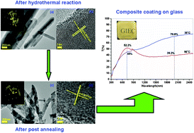
VO2 nanobelts with metal–semiconductor properties were prepared through low temperature hydrothermal reaction and post annealing. X-Ray diffraction (XRD), scanning electron microscopy (SEM), high resolution transmission electron microscopy (HRTEM), differential scanning calorimetry (DSC) and UV-vis-NIR spectrophotometry were employed to investigate the evolution of structure, morphology and properties of the VO2 nanobelts. The results illustrate that the pure VO2 (B) nanobelts can be obtained by hydrothermal reaction. The shape of the nanobelts evolves with hydrothermal temperature, time and reactant concentration. With the increasing of hydrothermal temperature from 160 °C to 200 °C, the nanobelts become homogenous and regular. The regular nanobelts are also obtained by the decrease of V2O5 concentration. Samples prepared at 200 °C over 48 h have superior morphology and crystallinity. After annealing, VO2 (B) can be transformed into VO2 (M), which is dependent on the hydrothermal conditions. Samples prepared at 160 °C over 48 h and 180 °C over 48 h can be transformed into VO2 (M) at 450 °C over 2 h, while samples obtained at 200 °C over 48 h should be annealed at 500 °C for 2 h. The nanobelts are transformed into irregular nanostructures, nanorods and nanobelts at the hydrothermal temperatures of 160 °C, 180 °C and 200 °C, respectively. However, samples prepared at 200 °C over 48 h with a V2O5 concentration of 0.0125 M can keep the intact nanobelts after annealing. The DSC analysis proves that the VO2 (M) shows good phase transition behavior around 68 °C and the phase transition temperature can be reduced to 58 °C by 0.5 at% tungsten doping. After mixing the VO2 (M) with acrylic resin, the visible transmission of the VO2 composite coating on glass is up to 52.2% and the solar modulation at 2000 nm is up to 31.5%, which means that it is a good candidate for smart windows.

Graphical abstract: A facile process to prepare one dimension VO2 nanostructures with superior metal–semiconductor transition

Article information

Article type
Paper
Submitted
08 Aug 2012
Accepted
05 Nov 2012
First published
06 Nov 2012

CrystEngComm, 2013,15, 1095-1106

A facile process to prepare one dimension VO2 nanostructures with superior metal–semiconductor transition

X. Xiao, H. Cheng, G. Dong, Y. Yu, L. Chen, L. Miao and G. Xu, CrystEngComm, 2013, 15, 1095 DOI: 10.1039/C2CE26262B

To request permission to reproduce material from this article, please go to the Copyright Clearance Center request page.

If you are an author contributing to an RSC publication, you do not need to request permission provided correct acknowledgement is given.

If you are the author of this article, you do not need to request permission to reproduce figures and diagrams provided correct acknowledgement is given. If you want to reproduce the whole article in a third-party publication (excluding your thesis/dissertation for which permission is not required) please go to the Copyright Clearance Center request page.

Read more about how to correctly acknowledge RSC content.

Social activity

Spotlight

Advertisements