
Robust atomic-structure of the 6 × 2 reconstruction surface of Ge(110) protected by the electronically transparent graphene monolayer†
 *b
Ruifen
Dou
*a
*b
Ruifen
Dou
*a
Abstract
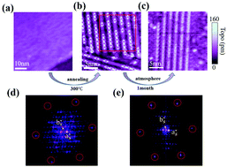
Wafer-scale growth of the unidirectional graphene monolayer on Ge surfaces has rejuvenated the intense study of the surfaces and interfaces of semiconductors underneath graphene. Recently, it was reported that the Ge atoms in the Ge(110) surface beneath a graphene monolayer underwent a rearrangement and formed an ordered (6 × 2) reconstruction. However, a plausible atomic model related to this (6 × 2) reconstruction is still lacking. Here, by using scanning tunnelling microscopy/spectroscopy (STM/S) and density functional theory (DFT) calculations, we deeply investigated the structural and electronic properties of the Ge(110) (6 × 2) surface encapsulated by a graphene monolayer. The (6 × 2) surface reconstruction was confirmed for the post-annealing-graphene-covered Ge(110) surface via STM, and was found to be quite air-stable, owing to the protection of the graphene monolayer against surface oxidation. Our study disclosed that the topographic features of the topmost graphene monolayer and the Ge(110) surface could be selectively imaged by utilizing suitable scanning biases. According to the STM results and DFT calculations, a rational ball-and-stick model of the (6 × 2) reconstruction was successfully provided, in which an elemental building block comprising two Ge triangles and two isolated Ge atoms adsorbed on the unreconstructed ideal Ge(110) surface. Local density of states of the graphene/Ge surface was explored via scanning tunneling spectroscopy (STS), presenting four well-defined differential conductance (dI/dV) peaks, protruding at energies of 0.2, 0.4, 0.6 and 0.8 eV, respectively. The four peaks predominantly originated from the surface states of the reconstructing adatoms and were well reproduced by our theoretical simulation. This result means that the Ge surface is very robust after being encapsulated by the epitaxial graphene, which could be advantageous for directly fabricating graphene/Ge-hybrid high-speed electronics and optoelectronics based on conventional microelectronics technology.
 Please wait while we load your content...

