Fermi-level pinning in methylammonium lead iodide perovskites†
Abstract
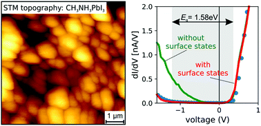
Hybrid organic inorganic perovskites are ideal candidates for absorber layers in next generation thin film photovoltaics. The polycrystalline nature of these layers imposes substantial complications for the design of high efficiency devices since the optoelectronic properties can vary on the nanometre scale. Here we show via scanning tunnelling microscopy and spectroscopy that different grains and grain facets exhibit variations in the local density of states. Modeling of the tunneling spectroscopy curves allows us to quantify the density and fluctuations of surface states and estimate the variations in workfunction on the nanometre scale. The simulations corroborate that the high number of surface states leads to Fermi-level pinning of the methylammonium lead iodide surfaces. We do not observe a variation of the local density of states at the grain boundaries compared to the grain interior. These results are in contrast to other reported SPM measurements in literature. Our results show that most of the fluctuations of the electrical properties in these polycrystalline materials arise due to grain to grain variations and not due to distinct electronic properties of the grain boundaries. The measured workfunction changes at the different grains result in local variations of the band alignment with the carrier selective top contact and the varying number of surface states influence the recombination activity in the devices.


 Please wait while we load your content...