Determination of optimum optoelectronic properties in vertically stacked MoS2/h-BN/WSe2 van der Waals heterostructures†
 b
and
Gang
Ouyang
*a
b
and
Gang
Ouyang
*a
Abstract
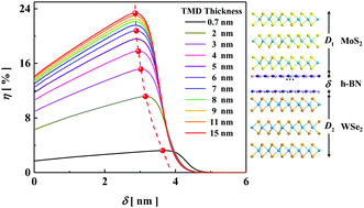
Current achievements show that inserting an insulator at the interface in van der Waals (vdW) heterostructures can improve the photoelectric conversion efficiency. However, the underlying mechanism of the intercalated insulator effect on photocarrier collection and recombination, etc., remains unclear at the atomic level. Herein, we investigate the influence of intercalated hexagonal boron nitride (h-BN) on the optoelectronic properties of MoS2/WSe2 vdW heterostructures based on the interface bond relaxation and detailed balance principles. It was found that the band offsets (barrier height) at the heterointerface decrease with increasing h-BN size and decreasing transition metal dichalcogenide (TMD) thickness. Moreover, the power conversion efficiency (PCE) in monolayer MoS2/11-layers h-BN/monolayer WSe2 can reach 3.23% and enhances with increasing thickness of TMDs. Also, the optimal thickness of h-BN in MoS2/h-BN/WSe2 decreases from 3.64 to 2.86 nm as the thickness of TMDs increases. Our results show that the PCE and open-circuit voltage of the MoS2/h-BN/WSe2 vdW heterostructure are obviously improved compared with the bilayer heterostructure without h-BN, and this further proves the feasibility of the intercalated insulator as a booster for highly efficient photovoltaic and optoelectronic nanodevices.
 Please wait while we load your content...

