Stacked indium oxide/zinc oxide heterostructures as semiconductors in thin film transistor devices: a case study using atomic layer deposition†
Abstract
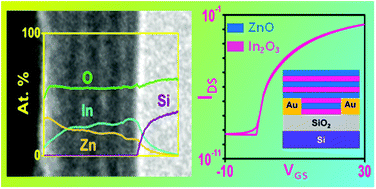
Multi-layer heterostructure oxide semiconductors employing a layer-by-layer deposition of alternating indium oxide and zinc oxide thin films generated via atomic layer deposition (ALD) are investigated for their feasibility into high performance thin film transistors (TFT). The successful deposition of uniform film thickness across the alternating indium oxide and zinc oxide deposition at 200 °C is achieved using trimethyl indium (TMI), diethyl zinc (DEZ) and water as oxidizing agent. The as-prepared polycrystalline material shows a conductive behaviour which upon additional mild annealing between 250–300 °C demonstrates a high TFT device performance. In addition, insights into the dependency of the defect passivation gradient within the multilayer upon thermal annealing of the oxide stack are presented. Studies towards an optimised film thickness result in a high device performance in enhancement mode with a saturation field-effect mobility (μsat.) of 6.5 cm2 V−1 s−1 and an on/off ratio (Ion/off) of 4.6 × 10⁷ using a deliberately large width to length channel ratio (W/L = 500). The TFT performance turned out to be dependent on the position of the individual oxide layers within the stack and the number of heterostructure stacks. These findings on the influence of semiconductor stack formation allow for a better understanding on the formation of the active semiconductor channel and serve towards the applicability of ALD based heterostructure metal oxide semiconductors in next generation electronics.


 Please wait while we load your content...