Fabrication of anisotropically arrayed nano-slots metasurfaces using reflective plasmonic lithography†
Abstract
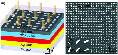
Nanofabrication technology with high-resolution, high-throughput and low-cost is essential for the development of nanoplasmonic and nanophotonic devices. At present, most metasurfaces are fabricated in a point by point writing manner with electron beam lithography or a focused ion beam, which imposes a serious cost barrier with respect to practical applications. Near field optical lithography, seemingly providing a high-resolution and low-cost way, however, suffers from the ultra shallow depth and poor fidelity of obtained photoresist patterns due to the exponential decay feature of evanescent waves. Here, we propose a method of surface plasmonic imaging lithography by introducing a reflective plasmonic lens to amplify and compensate evanescent waves, resulting in the production of nano resist patterns with high fidelity, contrast and enhanced depth beyond that usually obtained by near field optical lithography. As examples, a discrete and anisotropically arrayed nano-slots mask pattern with different orientations and a size of 40 nm × 120 nm could be imaged in photoresist and transferred successfully onto a metal layer through an etching process. Evidence for the pattern quality is given by virtue of the fabricated metasurface lens devices showing good focusing performance in experiments. It is believed that this method provides a parallel, low-cost, high-throughput and large-area nanofabrication route for fabricating nanostructures of holograms, vortex phase plates, bio-sensors and solar cells etc.


 Please wait while we load your content...