Breakdown of metallic single-wall carbon nanotube paths by NiO nanoparticle point etching for high performance thin film transistors
Abstract
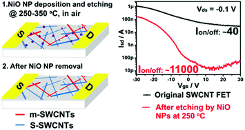
A selective and highly local etching of the metallic single-wall carbon nanotube (SWCNT) was demonstrated by using a NiO nanoparticle (NP) point etching technique. Following the NiO NP point etching at temperatures ranging from 250 to 350 °C, the current on/off ratios of the SWCNT field effect transistors (FETs) increased over 50-fold from ∼10 s to ∼104. Furthermore, the unavoidable drop in on-state current due to the reduction in current paths could be minimized to within one order of magnitude. Atomic force microscopy and Raman spectroscopy studies supported the view that the improvement in FET performance was attributed to the efficient and localized etching of metallic SWCNT paths solely around the NiO NPs, resulting in minimal damage to the semiconducting SWCNT networks.


 Please wait while we load your content...