Issue 11, 2014

Inverted process for graphene integrated circuits fabrication

Abstract

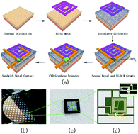
CMOS compatible 200 mm two-layer-routing technology is employed to fabricate graphene field-effect transistors (GFETs) and monolithic graphene ICs. The process is inverse to traditional Si technology. Passive elements are fabricated in the first metal layer and GFETs are formed with buried gate/source/drain in the second metal layer. Gate dielectric of 3.1 nm in equivalent oxide thickness (EOT) is employed. 500 nm-gate-length GFETs feature a yield of 80% and fT/fmax = 17 GHz/15.2 GHz RF performance. A high-performance monolithic graphene frequency multiplier is demonstrated using the proposed process. Functionality was demonstrated up to 8 GHz input and 16 GHz output. The frequency multiplier features a 3 dB bandwidth of 4 GHz and conversion gain of −26 dB.

Graphical abstract: Inverted process for graphene integrated circuits fabrication

Supplementary files

Article information

Article type
Paper
Submitted
30 Dec 2013
Accepted
02 Mar 2014
First published
04 Mar 2014

Nanoscale, 2014,6, 5826-5830

Author version available

Inverted process for graphene integrated circuits fabrication

H. Lv, H. Wu, J. Liu, C. Huang, J. Li, J. Yu, J. Niu, Q. Xu, Z. Yu and H. Qian, Nanoscale, 2014, 6, 5826 DOI: 10.1039/C3NR06904D

To request permission to reproduce material from this article, please go to the Copyright Clearance Center request page.

If you are an author contributing to an RSC publication, you do not need to request permission provided correct acknowledgement is given.

If you are the author of this article, you do not need to request permission to reproduce figures and diagrams provided correct acknowledgement is given. If you want to reproduce the whole article in a third-party publication (excluding your thesis/dissertation for which permission is not required) please go to the Copyright Clearance Center request page.

Read more about how to correctly acknowledge RSC content.

Social activity

Spotlight

Advertisements