
Impact of electrode recrystallization on the stability of organic transistors†
Shougang
Sun‡
ab,
Hanyang
Guan‡
c,
Jinbo
He‡
a,
Jiannan
Qi
a,
Xiaosong
Chen
 *a,
Liqiang
Li
ab and
Wenping
Hu
ab
*a,
Liqiang
Li
ab and
Wenping
Hu
ab
aKey Laboratory of Organic Integrated Circuit, Ministry of Education & Tianjin Key Laboratory of Molecular Optoelectronic Sciences, Department of Chemistry, Institute of Molecular Aggregation Science, Tianjin University, Tianjin 300072, China. E-mail: xschen2019@tju.edu.cn
bCollaborative Innovation Center of Chemical Science and Engineering (Tianjin), Tianjin 300072, China
cTianjin Xinhua High School, Tianjin 300204, China
First published on 16th May 2024
Abstract
Organic field-effect transistors (OFETs) have attracted wide attention due to their low cost, light weight, and mechanical flexibility. However, stability limits the practical application of OFETs. Although many strategies have been developed to stabilize organic semiconductor (OSC) films to improve the stability of OFETs, the impact of the electrode on the stability of OFETs has been ignored. Here, we demonstrate in detail the influence of recrystallization of polycrystalline metal electrodes on the stability of OFETs. Furthermore, the mechanically and thermally stable nano-graphene (NG) electrodes are prepared by the plasma-enhanced chemical vapor deposition (PECVD) method. The NG electrodes show good compatibility with OSCs, and the average mobility of bottom-gate bottom-contact dinaphtho[2,3-b:2′,3′-f]thieno[3,2-b]thiophene (DNTT) OFETs reaches 1.31 cm2 V−1 s−1. Moreover, the stable NG electrodes greatly improve the thermal stability of DNTT OFETs. This work proves that the stability of the electrodes plays a vital role in the stability of OFETs and provides a new idea for stabilizing OFETs.
 Xiaosong Chen | Xiaosong Chen graduated from Central China Normal University in 2011 with a bachelor's degree in physics. He obtained a PhD degree in science from East China Normal University in 2016. From 2016 to 2019, he was engaged in postdoctoral research in Fudan University and Shenzhen University. In 2019, he joined Tianjin University as an associate researcher. His research direction focuses on the device physics and stability of organic field-effect transistors. To date, he has published 21 SCI papers (including one in Science Advances, three in Nature Communications, and two in Advanced Materials, etc.) as the first or corresponding author. |
1. Introduction
Organic field-effect transistors (OFETs) have great potential applications in low-cost, flexible, and large-area electronics.1–6 Much progress has been made in terms of organic semiconductor (OSC) performance; however, serious stability problems remain in OFETs, which limit the commercialization.7–10 Several strategies have been developed to improve the stability of OSC films to stabilize OFETs, including the strain balance strategy,11 reducing thermal expansion coefficient mismatch,12 and blending high stability materials.13,14 However, the impact of electrodes on device stability has been neglected.Noble metals are widely used as source and drain electrodes in OFETs, but the noble metal electrodes prepared by evaporation and sputtering are polycrystalline formed by small metal grains.15,16 Due to the existence of vacancies, dislocations, and grain boundaries, polycrystalline metal electrodes spontaneously undergo recovery and recrystallization processes to release internal strain energy, resulting in electrode morphological evolution.17,18 As an important part of OFETs, electrode morphological evolution limits the stability of OFETs.19,20
Here, we prepare nano-graphene (NG) electrodes with good conductivity and thickness uniformity on the SiO2/Si substrate directly by the plasma-enhanced chemical vapor deposition (PECVD) method. The NG electrodes show excellent mechanical and thermal stability after high-frequency ultrasound and thermal annealing, while the metal electrodes fall off and recrystallize seriously. Moreover, bottom-gate bottom-contact (BGBC) dinaphtho[2,3-b:2′,3′-f]thieno[3,2-b]thiophene (DNTT) OFETs based on NG electrodes exhibit average mobility of 1.31 cm2 V−1 s−1 and maximal mobility of 1.68 cm2 V−1 s−1 with on/off ratios of 107, showing superior OTFT performance compared to that of Au electrodes in DNTT OFETs (0.21 cm2 V−1 s−1, 0.6 cm2 V−1 s−1 and on/off ratios of 104). A similar phenomenon has also been confirmed in other n-type and p-type small OSCs, showing good universality. More importantly, the thermal stability of DNTT OFETs with NG electrodes is greatly improved, and the device can still maintain high electrical properties after annealing at 180 °C.
2. Experimental
NG electrode fabrication
Nano-graphene films were prepared on SiO2/Si in a PECVD system. CH4 and H2 (purity > 99.99%) were used as the precursor with a flow rate of 50 sccm/10 sccm (150 mTorr). A clean SiO2/Si was placed in the growth zone and heated to 500 °C. The growth distance between the plasma generator and the sample growth area is 30 cm. At the same time, the plasma generator (30 W) is turned on, resulting in efficient growth of NG films for 30 min. The NG film was patterned by evaporation of aluminium (Al), then etched by oxygen plasma (50 W) for 20 minutes. The patterned film was etched with hydrochloric acid to obtain an NG electrode array.Device fabrication
All of the OSCs were purchased from Sigma-Aldrich (sublimed grade: > 99%). The wafers and NG electrode array were loaded into a vacuum oven (<0.01 bar) with 10 μL octadecyltriethoxysilane (OTS) (Sigma-Aldrich), and the vacuum oven stayed at 120 °C for 60 min, and was then cooled to room temperature. The OTS-treated 300 nm thick thermal SiO2 was obtained. The Au electrodes (20 nm thick) were thermally evaporated on the 300 nm SiO2/Si substrate as the source and drain electrodes for Au electrode OFETs. The OSC films of 30 nm were thermally deposited under a vacuum of 10−4 Pa at a rate of approximately 0.2 Å s−1 for both Au electrode and NG electrode substrates. The top contact OFETs were prepared by transferring Au electrodes (40 nm thick).Characterizations
All the measurements of OFETs were tested on an Agilent B1500 semiconductor parameter analyzer with a micromanipulator 6150 probe station at room temperature in air. The optical images were measured by VK-X1050 3D laser confocal microscopy. The surface topographies were measured by a Bruker Dimension ICON-PT in the air in tapping mode. X-ray photoelectron spectroscopy (XPS) was performed by a PHI 5000 Versaprobe. The Raman spectroscopy of the NG films was characterized by a Renishaw plc Wotton-under-Edge UK (laser wavelength: 532 nm). Ultraviolet photoelectron spectrometer (UPS) measurements were completed by a KRATOS Axis Ultra DLD spectrometer with He I (h = 21.22 eV) as the excitation source.3. Results and discussion
3.1 Growth of NG electrodes by PECVD
The radio frequency PECVD (13.56 MHZ) was used in this experiment. Fig. 1a illustrates the typical procedure of PECVD growth of NG on bare SiO2/Si by using CH4 and H2 as precursors. In a tubular furnace, the uniform NG films (Fig. 1b) were grown on SiO2/Si in 30 W plasma at 500 °C for 30 min. Furthermore, the obtained NG film is patterned by Al metal, and then exposed NG is etched by oxygen plasma, and Al is removed by hydrochloric acid to obtain the patterned NG electrode array (Fig. S1, ESI†). This method can only prepare the bottom NG electrode, and the top NG electrode can be prepared by transfer method. Fig. 1c shows a uniform and regular array of NG electrodes. To investigate the morphology of NG electrodes after etching and hydrochloric acid cleaning, we observed the complete structure and edge of the NG electrodes using atomic force microscopy (AFM). The NG electrodes show obvious boundaries and have an excellent uniform thickness of approximately 10 nm (Fig. 1d and e). | ||
| Fig. 1 NG electrodes grown by PECVD. (a) Schematic diagram of the PECVD system. (b) Optical image of bare SiO2/Si, and NG film grown on SiO2/Si, respectively. (c) Optical image of the NG electrode array. (d) AFM image of the edge of the NG electrode. (e) Thickness statistics of 15 NG electrodes. (f) XPS spectra of the NG electrode. (g) Raman spectra of the NG electrode. (h) I–V characteristic of the NG electrode. | ||
To confirm that the NG electrodes prepared by multiple processes are not polluted, the elemental composition of the NG electrode was examined by X-ray photoelectron spectroscopy (XPS). The distinct C 1s peak and hardly any impurity peaks indicate that a clean NG electrode has been obtained (Fig. 1f). The XPS C 1s spectrum of the NG film was fitted with sp2 carbon (284.1 eV) and C–H (285.0 eV) peaks (Fig. S2, ESI†). The dominant peak is the sp2 feature, confirming the graphitic structure of the grown material. According to Raman spectroscopy, the typical 1581 cm−1 (G-band) which originates from the sp2-hybridized hexagonal carbon atoms indicates that the NG electrode has a relatively high quality (Fig. 1g). Moreover, the measurement of conductivity of the NG electrode proves that the ultra-thin NG electrode has good conductivity of 1.5 × 10³ S cm−1 (Fig. S3, ESI† and Fig. 1h). Because the conductivity of OSC is relatively low21,22 (10−5–10−3 S cm−1), the NG electrodes have sufficient conductivity to be used as the source and drain electrodes.
3.2 The mechanical and thermal stability of the NG electrode
Generally, the electrode and the dielectric layer are adhered together by a weak interaction force, so the electrode would easily detach from the substrate,23,24 which has an adverse impact on the device stability. Graphene, a material with carbon atoms arranged by sp2-hybridized, is appropriate for preparing stable electrodes due to its high thermal stability and conductivity.25,26Fig. 2a and Fig. 2d show the morphology of the large-area NG electrode array and Au electrodes array after ultrasonic cleaning with distilled water at the same frequency and duration. Most of the Au electrodes have completely fallen off, while the NG electrodes can still maintain their complete morphology, indicating that the NG grown by PECVD has a strong interaction with the SiO2 dielectric layer, which is beneficial to prepare stable OFETs.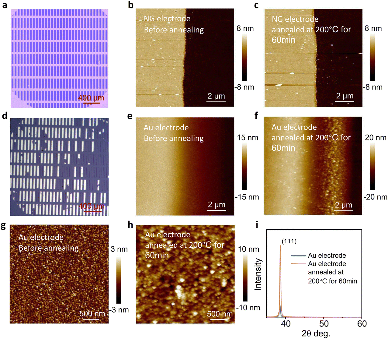 | ||
| Fig. 2 The stability of the electrode. (a) Optical images of the NG electrode array after ultrasonic cleaning at 53 kHz for 5 min. (b) and (c) AFM images of the NG electrode before and after annealing at 200 °C for 60 min. (d) Optical images of the Au electrode array after ultrasonic cleaning at 53 kHz for 5 min (e) and (f) AFM images of the Au electrode before and after annealing at 200 °C for 60 min. (g) and (h) AFM images of the Au electrode surface. (i) The XRD spectrum of the Au electrode before and after annealing. | ||
The large number of dislocation defects and grain boundaries in the polycrystalline metal electrodes make it easy to recrystallize,27,28 while graphene has excellent thermal stability because of its two-dimensional structure formed by sp2-hybridized carbon atoms.29 We further investigate the thermal stability of the electrode. After annealing at 200 °C for 60 min, the morphology of the NG electrodes has hardly changed (Fig. 2b and c). In the case of the Au electrodes, the gold grains of the electrodes become larger and the edge of the electrode shrinks obviously (Fig. 2e and f). The recrystallization of the polycrystalline gold film is easy to occur even at low temperature,30 and it will greatly affect its electrical properties, indicating that devices with polycrystalline Au electrodes are not suitable for device stability. In addition, we investigate the morphological changes of the Au electrode surface. After annealing at 200 °C for 60 min, the aggregation state of the Au electrode changes significantly (Fig. 2g and h). Moreover, the X-ray diffraction (XRD) spectrum confirms that the Au electrode is unstable, as the XRD peak (111) of the Au electrode is significantly enhanced after annealing (Fig. 2i).
Furthermore, the electrodes were annealed at a higher temperature. After being treated at 400 °C for 2 hours, the Au electrode shrinks seriously, while the NG electrode still shows excellent thermal stability (Fig. S4 and S5, ESI†). The excellent mechanical and thermal stability of the NG electrodes on the surface of the dielectric layer will be beneficial to the stability of OFETs.
3.3 High-performance OFETs based on the NG electrode
To investigate the influence of electrodes on the device, we fabricated BGBC DNTT OFETs with NG and Au electrodes (Fig. S6, ESI†). Fig. 3a is a schematic diagram of a BGBC structure DNTT OFET. Through the transfer curves, the NG electrode DNTT OFET shows higher on-state current and smaller threshold voltage (Fig. 3b and e). The threshold voltage of NG electrode DNTT OFET is approximately 6.8 V, and the mobility is as high as 1.68 cm2 V−1 s−1. Moreover, NG electrodes DNTT OFETs present much higher on-state current, indicating that OFETs based on NG electrodes have better electrical properties than OFETs based on Au electrodes (Fig. 3c and f).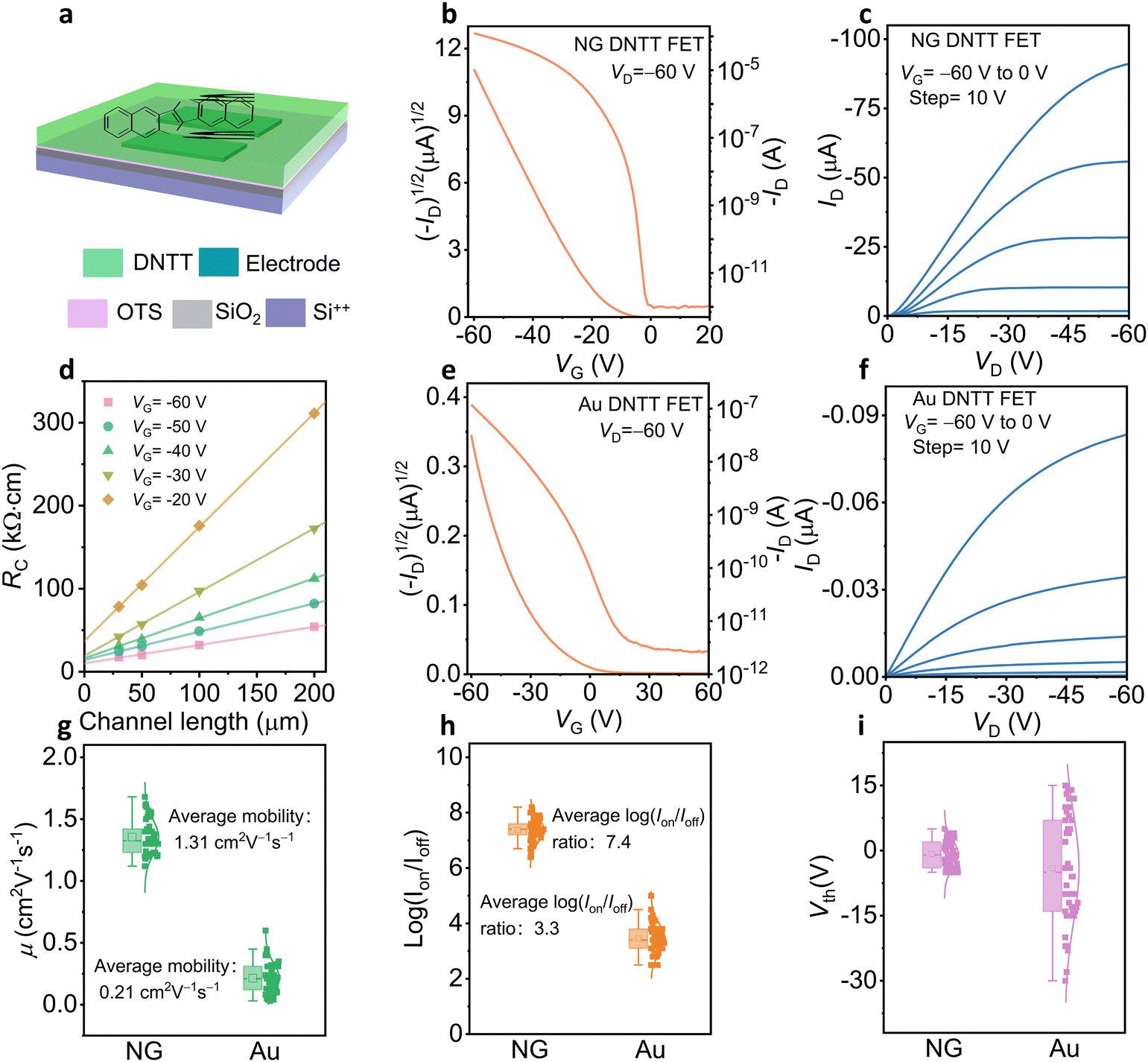 | ||
| Fig. 3 Electrical performance of the NG and Au electrode DNTT OFETs. (a) Schematic diagram of the BGBC structure OFET, and chemical structure of DNTT. (b) and (e) Transfer characteristics of the NG and Au electrode DNTT OFETs measured in the saturated regime of operation (VD = −60 V), respectively. (c) and (f) Output characteristics of the NG and Au electrode DNTT OFETs, respectively. (d) Rc extraction using the TLM method from the NG electrode DNTT OFETs. (g)–(h) Statistics of mobility, on/off ratio (Ion/Ioff), and threshold voltage (Vth) of 50 NG and Au electrode DNTT OFETs. | ||
Although the work function of the Au electrode31 (−5.1 eV) is closer to the HOMO level of DNTT than that of the NG electrode (−4.8 eV), and the injection barrier is smaller (Fig. S7 and S8, ESI†), the devices prepared with NG electrodes show better electrical properties. To investigate the factors affecting the electrical properties, we tested the electrical properties of OSCs films in the channel by transferring electrodes (Fig. S9, ESI†). The electrical properties of OSCs thin films in the channel are the same, indicating that the defects in the metal-semiconductor contact mainly affect the charge transport (Fig. S10, ESI†). In addition, the AFM images show that the OSC arrangement near the NG electrode edge is orderly, while the OSC arrangement near the Au electrode edge is disordered, indicating that the NG electrode is beneficial to the arrangement and charge transfer of OSCs at the interface of OSC and electrode (Fig. S11, ESI†). Moreover, the devices with the transferring electrodes show equal subthreshold slopes (SS), which further proves that the NG electrode is beneficial to reducing defects at the interface of OSC and electrode to improve device performance (Fig. S12, ESI†).
Furthermore, we extracted contact resistance (Rc) by the transfer-length-method32,33 (TLM) of the DNTT OFET with the NG electrode and it is 10 kΩ cm at VG = −60 V, while for the devices with the Au electrode, the Rc is 67 kΩ cm (Fig. 3d and Fig. S13, ESI†). The extraction Rc of Au electrode OFETs does not conform to a good linear relationship, which proves that the disorderly arrangement of molecules at the edge of the Au electrode makes it difficult to extract Rc accurately. Moreover, the electrical properties of 50 NG electrode DNTT devices show higher mobility (average mobility of 1.31 cm2 V−1 s−1 and a maximal mobility of 1.68 cm2 V−1 s−1), higher on/off ratio (107), and lower threshold voltage (Fig. 3g–i), while 50 Au electrode DNTT devices show low electrical performance with average mobility of 0.21 cm2 V−1 s−1, maximal mobility of 0.6 cm2 V−1 s−1 and on/off ratios of 104, indicating that the NG electrode is more conducive to improving the performance of OFETs. The transfer curves of p-type 2,9-didecyldinaphtho[2,3-b:2′,3′-f]thieno[3,2-b]thiophene (C10-DNTT) and n-type semiconductor N,N′-bis(n-octyl)-dicyanoperylene-3,4![[thin space (1/6-em)]](https://www.rsc.org/images/entities/char_2009.gif) :9,10-bis(dicarboximide) PDI-8CN2 with NG and Au electrode OFETs are shown in Fig. S14 (ESI†). Devices based on NG electrodes show higher on-state current and less hysteresis, suggesting that NG electrodes can effectively enhance the performance of a broad range of OSCs.
:9,10-bis(dicarboximide) PDI-8CN2 with NG and Au electrode OFETs are shown in Fig. S14 (ESI†). Devices based on NG electrodes show higher on-state current and less hysteresis, suggesting that NG electrodes can effectively enhance the performance of a broad range of OSCs.
3.4 The stable NG electrode enhances the stability of the OFET
Thermal annealing is an effective way to reduce the defects of OSCs and improve the performance of devices.34,35 However, due to the difference of thermal mismatch stress between OSCs and the substrate, cracks often appear in OSCs films after thermal annealing, which greatly affects the stability of the devices (Fig. S15, ESI†). In addition, the morphological evolution of polycrystalline Au electrodes may lead to electrode shrinkage and irreparable damage to the OSC film after annealing (Fig. S4, ESI†).To investigate the effect of the electrode on the stability of OFETs, we extracted the mobility of devices annealed at different temperatures for 30 min (Fig. 4). The mobility of the device with the NG electrode still maintains a high performance at 180 °C, proving that the NG electrode can realize the high temperature stability of OFETs. Fig. S16 (ESI†) shows the stabilizing effect of the NG electrode on OSC thin films after annealing. The NG electrode can effectively inhibit the cracking of the OSC films in the channel due to the excellent thermal stability, while the unstable polycrystalline Au electrode cannot effectively prevent cracking of the OSC films. Furthermore, we performed air stability measurement on NG and Au electrode OFETs. The results showed excellent air stability over 4 months with almost no degradation of NG electrode devices, indicating that stable NG electrodes can increase the storage stability of OFETs (Fig. S17, ESI†).
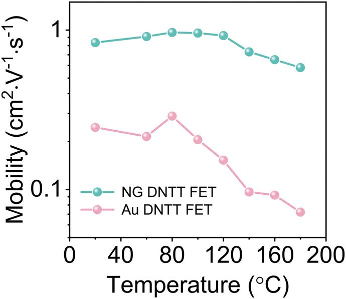 | ||
| Fig. 4 Variation of mobility of the NG and Au electrode DNTT OFETs after annealing at different temperatures for 30 min. | ||
Conclusions
In conclusion, we demonstrated that the recrystallization of polycrystalline metal electrodes plays a vital role in OFET stability. NG electrodes grown by PECVD have excellent mechanical and thermal stability, and their morphology remains unchanged after high temperature annealing. Utilizing the stable NG electrodes, the maximum mobility of BGBC DNTT OFETs rises to 1.68 cm2 V−1 s−1 with on/off ratios of 107. The NG electrode can effectively enhance the stability of OFETs, which provides a brand-new idea for realizing stable organic optoelectronic devices.Author contributions
Xiaosong Chen: conceptualization, formal analysis, methodology, investigation, funding acquisition, supervision, and writing – review & editing. Shougang Sun: conceptualization, formal analysis, methodology, and writing – review & editing. Hanyang Guan: formal analysis, methodology and writing – original draft. Jinbo He: formal analysis and writing – review & editing. Jiannan Qi: data curation and formal analysis. Liqiang Li: conceptualization, funding acquisition, and supervision. Wenping Hu: methodology and supervision. All authors discussed the results and commented on the manuscript.Conflicts of interest
There are no conflicts to declare.Acknowledgements
The authors are grateful to the National Key Research and Development Program (2022YFF1202700, 2018YFA0703200), National Natural Science Foundation of China (52203236, 52225304, 52073210, 21573277), Natural Science Foundation of Tianjin City (19JCJQJC62600, 19JCZDJC37400). This work is supported by the Fundamental Research Funds for the Central Universities. Xiaosong Chen graduated from Central China Normal University in 2011 with a bachelor's degree in physics. He obtained a PhD degree in science from East China Normal University in 2016. From 2016 to 2019, he was engaged in postdoctoral research in Fudan University and Shenzhen University. In 2019, he joined Tianjin University as an associate researcher. His research direction focuses on the device physics and stability of organic field-effect transistors. To date, he has published 21 SCI papers (including one in Science Advances, three in Nature Communications, and two in Advanced Materials, etc.) as the first or corresponding author.References
- J. Y. Oh, S. Rondeau-Gagné, Y.-C. Chiu, A. Chortos, F. Lissel, G.-J. N. Wang, B. C. Schroeder, T. Kurosawa, J. Lopez, T. Katsumata, J. Xu, C. Zhu, X. Gu, W.-G. Bae, Y. Kim, L. Jin, J. W. Chung, J. B. H. Tok and Z. Bao, Nature, 2016, 539, 411–415 CrossRef CAS PubMed.
- C. Jiang, H. W. Choi, X. Cheng, H. Ma, D. Hasko and A. Nathan, Science, 2019, 363, 719–723 CrossRef CAS PubMed.
- S.-J. Wang, M. Sawatzki, G. Darbandy, F. Talnack, J. Vahland, M. Malfois, A. Kloes, S. Mannsfeld, H. Kleemann and K. Leo, Nature, 2022, 606, 700–705 CrossRef CAS PubMed.
- S. Yuvaraja, A. Nawaz, Q. Liu, D. Dubal, S. G. Surya, K. N. Salama and P. Sonar, Chem. Soc. Rev., 2020, 49, 3423–3460 RSC.
- J. Song, H. Liu, Z. Zhao, P. Lin and F. Yan, Adv. Mater., 2023, 2300034 Search PubMed.
- Y. Xie, C. Ding, Q. Jin, L. Zheng, Y. Xu, H. Xiao, M. Cheng, Y. Zhang, G. Yang, M. Li, L. Li and M. Liu, SmartMat, 2024, e1261 CrossRef.
- H. Chen, W. Zhang, M. Li, G. He and X. Guo, Chem. Rev., 2020, 120, 2879–2949 CrossRef CAS PubMed.
- Y. Huang, Z. Wang, X. Chen, L. Li and W. Hu, Sci. Bull., 2023, 68, 1469–1473 CrossRef CAS PubMed.
- T. Salzillo, A. Campos, A. Babuji, R. Santiago, S. T. Bromley, C. Ocal, E. Barrena, R. Jouclas, C. Ruzie and G. Schweicher, Adv. Funct. Mater., 2020, 30, 2006115 CrossRef CAS.
- Y. Chen, W. Deng, X. Zhang, M. Wang and J. Jie, J. Phys. D: Appl. Phys., 2021, 55, 053001 CrossRef.
- X. Chen, Z. Wang, J. Qi, Y. Hu, Y. Huang, S. Sun, Y. Sun, W. Gong, L. Luo, L. Zhang, H. Du, X. Hu, C. Han, J. Li, D. Ji, L. Li and W. Hu, Nat. Commun., 2022, 13, 1480 CrossRef CAS PubMed.
- K. Kuribara, H. Wang, N. Uchiyama, K. Fukuda, T. Yokota, U. Zschieschang, C. Jaye, D. Fischer, H. Klauk, T. Yamamoto, K. Takimiya, M. Ikeda, H. Kuwabara, T. Sekitani, Y.-L. Loo and T. Someya, Nat. Commun., 2012, 3, 723 CrossRef PubMed.
- Z. Peng, N. Stingelin, H. Ade and J. J. Michels, Nat. Rev. Mater., 2023, 8, 439–455 CrossRef.
- A. Gumyusenge, D. T. Tran, X. Luo, G. M. Pitch, Y. Zhao, K. A. Jenkins, T. J. Dunn, A. L. Ayzner, B. M. Savoie and J. Mei, Science, 2018, 362, 1131–1134 CrossRef CAS PubMed.
- J. Yun, Adv. Funct. Mater., 2017, 27, 1606641 CrossRef.
- B. W. Stuart, X. Tao, D. Gregory and H. E. Assender, Appl. Surf. Sci., 2020, 505, 144294 CrossRef CAS.
- J. Chauvineau, P. Croce, G. Devant and M. Verhaeghe, J. Vac. Sci. Technol., 1969, 6, 776–779 CrossRef CAS.
- J.-H. Cho, H.-P. Ha and K. H. Oh, Metall. Mater. Trans. A, 2005, 36, 3415–3425 CrossRef.
- Z. Cheng, Y. Wang and D. M. O'Carroll, Org. Electron., 2019, 70, 179–185 CrossRef CAS.
- C.-W. Chu, S.-H. Li, C.-W. Chen, V. Shrotriya and Y. Yang, Appl. Phys. Lett., 2005, 87, 193508 CrossRef.
- M. Koopmans, M. A. T. Leiviskä, J. Liu, J. Dong, L. Qiu, J. C. Hummelen, G. Portale, M. C. Heiber and L. J. A. Koster, ACS Appl. Mater. Interfaces, 2020, 12, 56222–56230 CrossRef CAS PubMed.
- A. D. Scaccabarozzi, A. Basu, F. Aniés, J. Liu, O. Zapata-Arteaga, R. Warren, Y. Firdaus, M. I. Nugraha, Y. Lin, M. Campoy-Quiles, N. Koch, C. Müller, L. Tsetseris, M. Heeney and T. D. Anthopoulos, Chem. Rev., 2022, 122, 4420–4492 CrossRef CAS PubMed.
- Y. Liu, J. Guo, E. Zhu, L. Liao, S.-J. Lee, M. Ding, I. Shakir, V. Gambin, Y. Huang and X. Duan, Nature, 2018, 557, 696–700 CrossRef CAS PubMed.
- G. Kwon, Y.-H. Choi, H. Lee, H.-S. Kim, J. Jeong, K. Jeong, M. Baik, H. Kwon, J. Ahn, E. Lee and M.-H. Cho, Nat. Electron., 2022, 5, 241–247 CrossRef CAS.
- X. Huang, Z. Yin, S. Wu, X. Qi, Q. He, Q. Zhang, Q. Yan, F. Boey and H. Zhang, Small, 2011, 7, 1876–1902 CrossRef CAS PubMed.
- J. H. Chu, D. H. Lee, J. Jo, S. Y. Kim, J.-W. Yoo and S.-Y. Kwon, Adv. Funct. Mater., 2016, 26, 7367 CrossRef CAS.
- S. Kang, I. Bernstein and C. Bauer, Scr. Metall., 1976, 10, 693–696 CrossRef CAS.
- A. A. Tiamiyu, E. L. Pang, X. Chen, J. M. LeBeau, K. A. Nelson and C. A. Schuh, Nat. Mater., 2022, 21, 786–794 CrossRef CAS PubMed.
- A. S. Barnard and I. K. Snook, J. Chem. Phys., 2008, 128, 094707 CrossRef PubMed.
- J. P. Chauvineau, P. Croce, G. Devant and M. F. Verhaeghe, J. Vac. Sci. Technol., 1969, 6, 776–779 CrossRef CAS.
- V. Mansfeldova, M. Zlamalova, H. Tarabkova, P. Janda, M. Vorokhta, L. Piliai and L. Kavan, J. Phys. Chem. C, 2021, 125, 1902–1912 CrossRef CAS.
- J. W. Borchert, R. T. Weitz, S. Ludwigs and H. Klauk, Adv. Mater., 2022, 34, 2104075 CrossRef CAS PubMed.
- J. W. Borchert, B. Peng, F. Letzkus, J. N. Burghartz, P. K. Chan, K. Zojer, S. Ludwigs and H. Klauk, Nat. Commun., 2019, 10, 1119 CrossRef PubMed.
- C. Wang, H. Dong, L. Jiang and W. Hu, Chem. Soc. Rev., 2018, 47, 422–500 RSC.
- M. O’Neill and S. M. Kelly, Adv. Mater., 2011, 23, 566–584 CrossRef PubMed.
Footnotes |
| † Electronic supplementary information (ESI) available. See DOI: https://doi.org/10.1039/d4tc01364f |
| ‡ These authors contributed equally to this work. |
| This journal is © The Royal Society of Chemistry 2024 |