
 Open Access Article
 This Open Access Article is licensed under a
 Creative Commons Attribution 3.0 Unported Licence
MXenes as a hole transport interfacial layer for efficient and air-stable quasi-2D perovskite solar cells†
Sanjay
Sahare‡
 *a,
Mykhailo
Solovan‡
a,
Marina
Smirnova
bc,
Błażej
Scheibe
c,
Mariusz
Jancelewicz
c,
Grzegorz
Nowaczyk
c,
Mateusz
Kempiński
a and
Marcin
Ziółek
*a
*a,
Mykhailo
Solovan‡
a,
Marina
Smirnova
bc,
Błażej
Scheibe
c,
Mariusz
Jancelewicz
c,
Grzegorz
Nowaczyk
c,
Mateusz
Kempiński
a and
Marcin
Ziółek
*a
aFaculty of Physics, Adam Mickiewicz University, Uniwersytetu Poznanskiego 2, Poznan 61-614, Poland. E-mail: sanjay.sahare@amu.edu.pl; marcin.ziolek@amu.edu.pl
bFaculty of Chemistry, Adam Mickiewicz University, Uniwersytetu Poznanskiego 8, Poznan 61-614, Poland
cNanoBioMedical Centre, Adam Mickiewicz University, Wszechnicy Piastowskiej 3, Poznan 61-614, Poland
First published on 31st May 2024
Abstract
Despite the high performance of bulk hybrid perovskites, the material/device stability is a critical issue originating from the perovskites’ degradation when exposed to an open-air atmosphere. 2D/quasi-2D perovskite materials have attracted much attention due to their high stability under ambient conditions compared to the bulk perovskite. Along with 2D perovskite, various charge transport materials, and additives were also employed in perovskite solar cells (PSCs). We carried out one such approach in this work, where Ti3C2Tx a typical representative of the 2-D family, called MXenes, has been employed as a passivation/interfacial layer between the quasi-2D perovskite and the hole transport layer. A PSC, passivated with MXenes, shows over 9% relative improvement in the performance and very high stability (∼99%) in an open-air atmosphere over 50 days as compared to its pristine device. The detailed investigation suggests the role of MXene as a passivator, an energy aligner, and a barrier to reduce the non-radiative recombination loss, provide pathways for effortless hole transportation, and protect from external environmental factors respectively. Moreover, transient absorption studies reveal that adding MXenes also affects the distribution and lifetime of quasi-2D phases in PSCs. As we delve into specific applications, such as the integration of MXenes as passivator/HTL interfacial layers in 2-D PSCs, we unlock the potential for enhanced device performance, showcasing MXenes as a driving force in the evolution of stable solar cell technologies.
1. Introduction
Hybrid halide perovskite solar cells (PSCs) have been heralded as one of the most promising emerging technologies in the last decade. The unswerving progress in terms of photon to current conversion efficiency (PCE) of the device has increased dramatically over 26%1 through material and device engineering, but still the cost for electricity generation is low compared to even fossil fuels. Such exceptional progress in PSCs is considered to replace some state-of-the-art energy generation technologies in the photovoltaic market including silicon and gallium arsenide solar cells. However, device stability is a major concern from the prospect of commercialization. This nerve has been held by plenty of researchers and remarkable efforts have been made in the modification of perovskite composition2,3 and interfacial layers/charge collecting electrodes,4–6 passivating them with organic molecules,7 oxides, and 2D materials,8,9 and device encapsulations.10,11 Perovskite is a key component in PSCs that plays a crucial role in photon absorption, charge generation, transportation, and their recombination dynamics; which consequently decides the performance and stability of the device. Hence, it is essential to obtain high-quality perovskite films, else further processes are required to eliminate defects/traps and achieve highly crystalline perovskites.12,13Another approach for the stable device is to reduce the dimensionality of the perovskite, and many such efforts have been highlighted in the literature.14,15 Especially, the 2D Ruddlesden–Popper (RP) perovskite has gained more attention due to leveraging its unique structure to enhance stability and tuneable properties for the improvement of photovoltaic performance. A layered RP phase with the general formula of R2(A)n−1BnX3n+1 (n = 1, 2, 3, … where n is the number of layers) can be obtained upon the addition of big cation salts in the perovskite precursors.16,17 Recently, Lee et al. have demonstrated performance enhancement with stability using a 2D phenylethyl ammonium salt-based perovskite (PEA2PbI4).18 Mainly, with these 2D perovskite structures, the crystallization orientation can be controlled easily and rapid carrier transportation can be achieved in the device.15 However, maintaining efficient charge transport and preventing interlayer charge recombination are challenging tasks in 2D RP-based devices.
Nevertheless, a PSC consists of multiple layers and interfaces that play a vital role in the device performance and stability. Electronic and physical processes including energy alignment,19 charge transport at the interfaces,20 energy barriers,21 interfacial defects,20 and poor adhesion between adjacent layers22 have significant impacts on the photoelectrical properties of PSCs. The choice of charge transport layers (CTLs) and their modification has gained much attention to alter the above-mentioned processes, which eventually enhances charge injection and collections at the perovskite/CTL interfaces. Semiconducting 2D materials, for instance, MoS2, WS2, SnS2, graphene, MXene, etc. have tremendous potential as CTLs and are consistently used in PSCs.23–26 Also, these 2D CTLs show dual functionality, where they can be used as a passivator to perovskite, and align the energy level between the perovskite and the CTL.27 MXenes are one of the rapidly emergent 2D materials, which can be easily integrated with other materials owing to their profusion surface terminated functionalities.28 Amusing chemistry and surface terminations tune the finest properties and make MXenes a unique 2D material with enormous possible applications ranging from energy generation and storage to healthcare.29,30 Especially, MXenes can tailor the electronic structure such as the work function and bandgap of the host material wherever it may introduced.31,32 These potentials drive solar cell applications, where many heterojunctions perform their individual and collective role in energy generation. Work function tuning can attain the appropriate energy level alignment in PSCs, which leads to creating an ideal energy offset between the active layer and the CTL. This can be useful to induce built-in potential for efficient charge collection at the electrode. Many research groups have tried to incorporate MXenes as an additive in the perovskite, and also to modify the ETL.32–35 However, all attempts have been made with the 3D/bulk phase of perovskites. There are very few attempts in the literature, where 2D MXenes were used with 2D RP PSCs.36,37 Recently, Wang et al. demonstrated a MXene incorporated RP perovskite that achieved around 15% performance improvement as compared to its counterpart devices.36 Similarly, Yang et al. used aTi3C2Tx in Pb-free dye-sensitized 2D Cs2AgBiBr6 perovskite solar cell, where it alters the work function and weakens the Fermi level pinning.38 Zhang et al. have synthesized oxygen plasma treated Nb2CTx MXene and used it as an HTL in PSCs that increased its work function due to an –O terminated functional group.39 Furthermore, they fabricated an amino-functionalised Nb2CTx MXene, and interestingly this time, it was used as an ETL in PSCs to enhance the device performance along with its stability.40 The fact is that different functional groups can alter (increase or decrease) the work function and the HOMO/LUMO energy level, which will be used as an ETL or an HTL.
In this work, we are using Ti3C2Tx MXene for the first time with 2D RP perovskite as an interfacial layer between the perovskite and the HTL in the regular (normal) structure (n–i–p). The PSC with MXene shows ∼9% performance improvement as compared to its pristine device with substantial stability under open-air conditions over 50 days. As we delve into specific applications, such as the integration of MXenes as hole transport interfacial layers in 2D perovskite solar cells, we unlock the potential for enhanced device performance, showcasing MXenes as a driving force in the evolution of materials for advanced technologies. Furthermore, we investigate the photophysical properties using pump–probe techniques. In this research, we aim to understand the intricacies of interactions of MXenes within solar cell architectures and their contribution to the quest for more efficient and sustainable energy solutions.
2. Experimental work
2.1. Materials
The fluorine-doped tin oxide (FTO) substrates (∼7–8 Ω □−1) were purchased from OPVtech, China. TiO2 paste and 4F-phenethylammonium iodide (4F-PEAI) were bought from Greatcell Solar Materials, Australia. The chemical precursors for perovskite and CTL, viz. titanium diisopropoxide bis(acetylacetonate) [(CH3)2CHO]2Ti(C5H7O2)2, lead(II) iodide (PbI2), methylammonium iodide (MAI), lithium-bis(trifluoromethanesulfonyl)imide (LiTFSI), ammonium chloride, tert-butylpyridine (t-BP), anhydrous N,N-dimethylformamide (DMF), thiosemicarbazide (TSC), chlorobenzene, acetonitrile, and 2,2′,7,7′7-tetrakis-(N,N-di-p-methoxyphenylamine)-9,9′-spiroobifluorene (Spiro-OMeTAD) were purchased from Merck/Sigma Aldrich.2.2. Synthesis of MXenes
One gram of LiF (98.5%, Alfa Aesar) was slowly dissolved in 10 mL of 12 M HCl (35–38%, POCH). Subsequently, 1.0 g of Ti3AlC2 (Carbon, Ukraine) MAX phase powder was gradually added to a premixed etchant solution and stirred at 300 rpm for 24 h at 35 °C. The reacted solution containing multi-layered Ti3C2Tx MXenes was washed with ultrapure MilliQ (13.2 MΩ cm−1) type-1 water (t1-H2O) and centrifuged at 3500 rpm for 10 min. Next, the supernatant was decanted, and MXenes were re-dispersed in 40 mL of t1-H2O by manual shaking. The washing procedure was repeated until the pH of the supernatant reached a value of ∼6. To obtain the colloidal solution of MXenes, the material was re-dispersed in 300 mL of fresh t1-H2O and sonicated under an Ar flow for 1 h in a sonication bath below 10 °C. As-obtained colloidal solution of MXenes was centrifuged at 10![[thin space (1/6-em)]](https://www.rsc.org/images/entities/char_2009.gif) 000 rpm for 1 h to purify MXenes from salt contaminants. Then, the supernatant was discarded, while the pellet was re-dispersed afresh and centrifugated at 2500 rpm to remove the remaining multi-layered MXenes and unetched MAX phase impurities. Thus, the pellet was discarded and the supernatant was filtered through a polycarbonate membrane (0.2 μm, Cyclopore, Whatman). Purified MXenes were re-dispersed in 10 mL of t1-H2O, purged with Ar, and stored at 4 °C for further usage. 1500 μL of colloidal solution was divided into three pre-weighed Eppendorf test tubes (1.5 mL), freeze-dried, and weighed to calculate the weight of the solid material per mL of MXenes’ colloidal solution.
000 rpm for 1 h to purify MXenes from salt contaminants. Then, the supernatant was discarded, while the pellet was re-dispersed afresh and centrifugated at 2500 rpm to remove the remaining multi-layered MXenes and unetched MAX phase impurities. Thus, the pellet was discarded and the supernatant was filtered through a polycarbonate membrane (0.2 μm, Cyclopore, Whatman). Purified MXenes were re-dispersed in 10 mL of t1-H2O, purged with Ar, and stored at 4 °C for further usage. 1500 μL of colloidal solution was divided into three pre-weighed Eppendorf test tubes (1.5 mL), freeze-dried, and weighed to calculate the weight of the solid material per mL of MXenes’ colloidal solution.
2.3. Device fabrication
Prior to complete PSC fabrication, the fluorine-doped tin oxide (FTO) on the glass substrate was thoroughly cleaned with successive sonication in detergent, deionized water, acetone, and ethanol for 15 min each. Cleaned substrates were further treated with UV-ozone, which helps to remove the organic residue and increase their wettability. The compact TiO2 layer was formed by the spray-pyrolysis technique at 450 °C, where titanium diisopropoxide was used as a precursor solution in ethanol (1 mL + 14 mL EtOH). The mesoporous TiO2 (m-TiO2) layer from titania paste in ethanol (1:6 w/w) was deposited using the spin coating method in the open air at 2000 rpm for 10 s and then annealed at 500 °C for 30 minutes. This process forms m-TiO2 with a good interface between compact and mesoporous layers. The combination of compact and m-TiO2 layers acts as an ETL. Subsequently, quasi-2D perovskites [(4F-PEA)2MA4Pb5I16] were synthesized by mixing the individual precursors including 4F-PEAI, MAI, and PbI2 in a 2:4:5 (0.7 M) stoichiometric ratio in DMF. NH4Cl and TSC were used as coordinating additives in the precursor solution of 20% and 5% with respect to PbI2, respectively. These additives can arrange the perpendicular orientation of perovskite crystallites.41 Films were deposited using a spin coater on an m-TiO2 layer under a dry air atmosphere for 45 s at 4000 rpm. Just 10 s before the end of this process, chlorobenzene was used as an antisolvent for rapid crystallization followed by annealing at 150 °C for 10 min. A Ti3C2Tx, MXene (0.5 mg mL−1 in chlorobenzene) was used as an interfacial layer between the 2D perovskite and the HTL and then deposited similarly to antisolvent in the prior case. The whole process of perovskite deposition was carried out under a dry-air atmosphere. As HTL, Spiro-OMeTAD solution, (40 mM in chlorobenzene) with additives (17.5 μL mL−1 of 520 mg LiTFSI per mL in acetonitrile solution and 28.8 μL mL−1 4-tert-buthylpyridine) was also spin coated (4000 rpm, 30 s) and stored overnight in the same atmosphere. Finally, Au (∼75 nm) was deposited on the Spiro-OMeTAD with a DC sputtering system for 180 s at 30 mA. A complete PSC with a regular structure: FTO glass/c-TiO2/m-TiO2/quasi 2D perovskite/MXene/Spiro-OMeTAD/Au was formed and ready for further electrical measurements.
2.4. Material and device characterizations
MXenes were characterized by powder X-ray diffraction (XRD) analysis on an Empyrean (PANalytical) diffractometer using Cu Kα radiation (1.54 Å) and a PIXcel 3D detector, operating in the Bragg–Brentano geometry. The 2θ scans were recorded in angles ranging from 10 to 90 (°2 Theta) with a step size of 0.013 (deg) and continuous scan mode. The vibrational properties were examined by micro-Raman spectroscopy (via Raman microscope; Renishaw) with a 50× objective (Leica) at λ = 514 nm. Moreover, the morphological analyses of the MXene and perovskite devices were carried out using a thermal emission scanning electron microscope (SEM, JEOL-7001) with the acceleration voltage varying from 5 to 15 kV. An AFM (Park Systems XE7) was employed to check the topography of the perovskite in the non-contact mode. The steady-state absorption of PSCs was measured using a UV-Vis-NIR JASCO V-770 spectrophotometer. The whole device (except the Au electrode) has been considered for the UV-Vis absorption measurement. The UV-Vis region was investigated using an additional 150 mm integrating sphere (ILN-925). The stationary photoluminescence was measured using a spectrometer Hitachi F-7000. Current–voltage characteristics were recorded using a potentiostat (model M101, Autolab) coupled to a photoelectric spectrometer, equipped with a solar simulator (Instytut Fotonowy, Poland). The simulator provides standard 1 sun illumination conditions using an Xe lamp and AM1.5G filter (calibrated by silicon solar cell 15151, ABET). Impedance spectroscopy data were analyzed using an M101/FRA32M response analyzer module (Autolab) under 1 sun illumination (near short-circuit conditions) and in the dark. A voltage perturbation of 10 mV was used at different applied bias voltages, in the frequency range from 1 to 106 Hz. To know the charge carrier dynamics and the distribution of low dimensional perovskite phases, a femtosecond transient absorption (TA) spectroscopy experiment was performed for PSCs using 1 kHz repetition rate and 0.4 ps response function setup delivered using an Ultrafast Systems (Spectra-Physics laser system and Helios spectrometer). The samples (complete solar cells) were excited at 475 nm using different pump pulse fluences (from 1 to 1500 μJ cm−2), while for probing white light in the range of 500–830 nm was used. TA data were globally analyzed using Surface Explorer (Ultrafast Systems) software. The program allowed fitting a multi-exponential function (convoluted with response function) to the kinetic vectors of a selected number of singular values. Finally, the characteristic time constants and the wavelength-dependent amplitudes associated with them were obtained.3. Results and discussion
3.1. Structural and morphological analysis of MXenes and passivated 2D perovskite
The synthesized MXenes were evaluated using XRD spectra, where Fig. 1 confirms the successful exfoliations from the MAX phase. Generally, the signature peak of the MAX phase is observed at 2θ = 39°,42 which is completely missing in the synthesized 2D structure. The purity of the MXene sample was confirmed by the presence of a strong (002) peak at 6.7° of the XRD pattern, suggesting a lack of remaining impurities such as TiC or α-Al2O3 microparticles. The interlayer (d) spacing of Ti3C2Tx MXene was calculated in the range of 13.54–13.88 Å. The increased d-spacing is due to the structural expansion from etching and substitution of Al atoms with –F, and –OH/![[double bond, length as m-dash]](https://www.rsc.org/images/entities/char_e001.gif) O terminating groups. The inset of Fig. 1(a) demonstrates the SEM images of the MAX phase and formed single-layer MXene. The molecular vibrations associated with the bonding between atoms were probed through Raman spectroscopy, and a typically measured Raman spectrum of Ti3C2Tx was analyzed and presented in Fig. 1b. An exfoliated single layer Ti3C2Tx shows its typical in-plane (E1g) and out-of-plane (A1g) Raman-active modes in the range of 100–800 cm−1. In particular, upon the removal of Al from the MAX phase, the vibrational mode A1g associated with Ti, C, Tx (O); and C of the MXene was observed at ca. 204 and 734 cm−1 respectively. Other vibrational mode E1g associated with the functional surface species Tx observed at 385 cm−1 and 615 cm−1.
O terminating groups. The inset of Fig. 1(a) demonstrates the SEM images of the MAX phase and formed single-layer MXene. The molecular vibrations associated with the bonding between atoms were probed through Raman spectroscopy, and a typically measured Raman spectrum of Ti3C2Tx was analyzed and presented in Fig. 1b. An exfoliated single layer Ti3C2Tx shows its typical in-plane (E1g) and out-of-plane (A1g) Raman-active modes in the range of 100–800 cm−1. In particular, upon the removal of Al from the MAX phase, the vibrational mode A1g associated with Ti, C, Tx (O); and C of the MXene was observed at ca. 204 and 734 cm−1 respectively. Other vibrational mode E1g associated with the functional surface species Tx observed at 385 cm−1 and 615 cm−1.
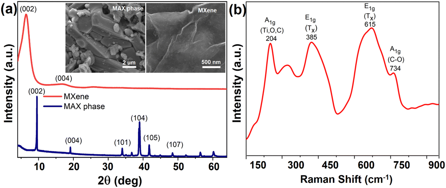 | ||
| Fig. 1 (a) XRD spectra of MAX phase and MXene, inset figures show SEM images that depict their morphology. (b) Raman spectrum of MXene. | ||
The obtained MXene was used in the regular structure solar cell, where it acts as a passivator for the perovskite and an interfacial layer between the perovskite and the HTL. The morphology of the quasi-2D perovskite [(4F-PEA)2MA4Pb5I16] is shown in Fig. 2a, where one can depict a pinhole structure. This can act as a recombination center in the PSCs, leading to a reduction in the overall performance. To overcome this, the MXene layer has been used as a passivator for 2D-perovskite that can alter the surface layer and form a pinholes-free surface (Fig. 2b). There might be a physical interaction between MXene and 2D-perovskites, which contributed to the adhesion of the passivation layer to the perovskite surface and stabilized the passivation over time.43,44 The AFM images (Fig. 2c and d) also confirm the passivation that makes the perovskite surface smoother than its counterpart. The MXene passivation forms a thin layer on 2D-perovskite, hence unable to detect underneath the perovskite layer.
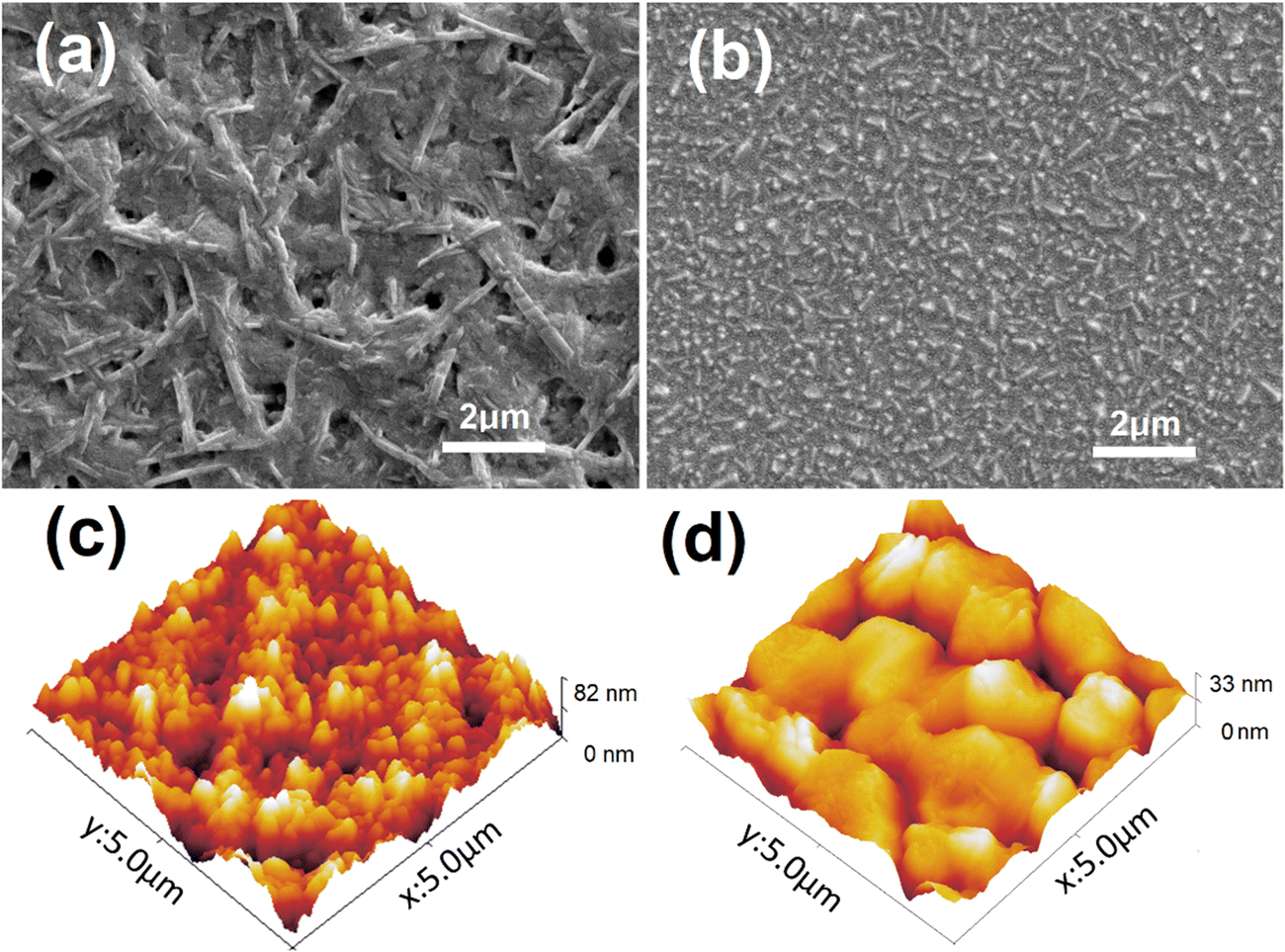 | ||
| Fig. 2 SEM images of (a) 2D-perovskite, and (b) MXene passivated 2D-perovskite; AFM images of (c) 2D-perovskite, and (d) MXene passivated 2D-perovskite. | ||
3.2. Electrical characterization
For investigating the effect of MXene as an interfacial layer between 2D-perovskite and HTL, PSCs with a configuration of FTO glass/c-TiO2/m-TiO2/quasi-2D-perovskite/MXene/Spiro-OMeTAD/Au (Fig. 3a, inset) was formed and measured under the standard 1 sun conditions. The MXene passivated/interfacial layered device showed better performance as compared to the reference PSCs. The J–V curves indicated in Fig. 3a (measured in the reverse direction at 100 mV s−1 rate using a mask of 0.08 cm2 aperture) are from the best device among many devices in different batches. It shows the highest performance of the MXene-based PSC is 7.4%, which is ∼9% higher than the reference PSCs (PCE = 6.8%). The quasi-2D perovskite-based PSCs generally demonstrate less PCE as compared to the 3D perovskite structures, though 2D perovskite provides better stability.5,45 All device fabrication was carried out under dry air conditions. Similarly, the regular structure, large area of Au electrode, and sputtering deposition method are also probable sources for the low fill factor of the device, and hence efficiency as well. However, the presented data based on the 2D perovskite is enough to distinguish the effect of the MXene in PSCs. One can observe in Fig. 3a that the Voc of the MXene-based device is higher than the reference device, which has been contributed by the increased built-in potential (Vbi) as shown in Fig. 3b. It is obvious that the HOMO of the MXene is deeper46,47 than the HOMO of Spiro-OMETAD, which causes an increase in the built-in potential in MXene-based PSCs. The probable energy band alignment depicts the charge transfer process in the device and is shown in the inset of Fig. 3b. The MXene layer can adjust the energy level between 2D-perovskite and HTL, which provides a reliable pathway for hole transfer and improves performance. The average electrical parameters from several devices have been measured and plotted together as shown in Fig. 3c. Along with the Voc, the current density of devices has also been increased, which leads to enhanced device performance. The results are quite repeatable since the average PCE is 6.45% in reference devices and 7.18% in MXene-based devices. It should be noted that our devices show relatively low PCE compared to the best reports for the same quasi-2D perovskite composition.45 However, all high-efficiency reports refer to the inverted structure of the perovskite with the HTL deposited on FTO glass. PCE above 19% has been also reported in the normal configuration but with 2D perovskite of another composition (with guanidinium cation) and using SnO2 as ETL.48 To the best of our knowledge, in this work, we report the highest PCE of this quasi-2D perovskite composition for normal configuration with mesoporous TiO2 layer as bottom ETL. One of the reasons behind our choice is that we focused on the effect of the MXene on HTL which is easier to be implemented in the normal configuration. Probably, the main reason for low PCE in this normal configuration with respect to the best one lies in the poor interaction of the 2D structure with TiO2. The mesoporous TiO2 layer is most probably also responsible for the moderate hysteresis in our devices (hysteresis index HI = 0.24 +/− 0.05, independent of the presence or absence of MXene; an example is shown in Fig. S1 in the ESI†), which has been frequently reported for many perovskite solar cells.49–51 Nevertheless, it is important to note that, 2D perovskite passivated with MXene helps to reduce the pinhole defects, and subsequently carrier recombination which leads to enhance the current density.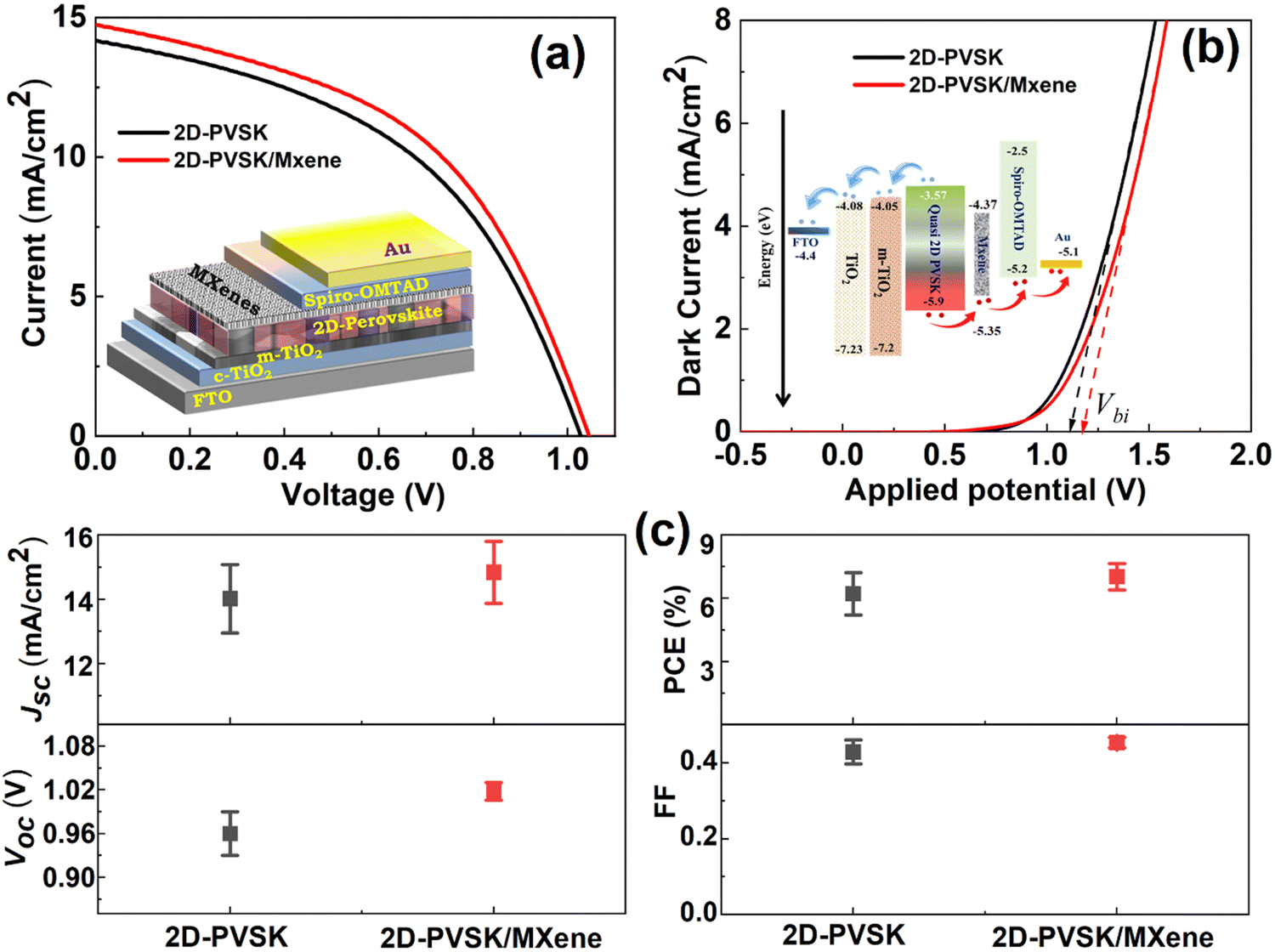 | ||
| Fig. 3 Current density–voltage curves under (a) light illumination and (b) dark. Inset figures demonstrated a device's structure, and its band energy alignment to show probable charge transfer. (c) Evaluated average parameters for several devices from J–V curves under light illumination. | ||
Furthermore, to confirm the passivation effect on the recombination centers (pinhole defect), steady-state measurements of the Voc have been performed under different intensities of light, which is an efficient qualitative method to determine the dominant mechanism of recombination losses in photovoltaic devices.52 The slope of the Vocversus light intensity is a pointer to the dominant recombination mechanisms. The 2D-PVSK-based device revealed a slope of 1.59 kT q−1 (Fig. 4), indicating a large relative contribution of trap-assisted Shockley Reed Hall (SRH) recombination losses due to the bulk trap centers in the active layer. However, upon MXene passivation, the PSC illustrated the reduction of slope to 1.48 kT q−1 due to plummeting the trap-states by filling these bulk trap centers near the interface. Moreover, the detailed quantitative analysis of recombination dynamics has been performed, and trap densities have been calculated for both devices using impedance spectroscopy53,54 as shown in Fig. 4b. The density of bulk (Nt,b) and surface (Nt,s) trap states have reduced in the MXene passivated device as compared to the pristine device under 1sun illumination (by about 10–15%). This is clearly indicating the effective passivation of MXene over the 2D-PVSK film. The detailed calculation and other indirect parameters have been shown in the ESI† (Fig. S2 and S3) The obtained results depict a positive effect of the MXene on the PSC, as recombination is reduced and improves the performance. This result is also well supported by the current density–voltage curves as shown in Fig. 3.
 | ||
| Fig. 4 (a) The Voc as a function of the light intensity for two different PSCs, (b) measured and calculated recombination current under 1 sun illumination. | ||
3.3. UV-Vis absorption and quantum efficiency
The absorption properties of the 2D-perovskite film upon MXene passivation were investigated through a stationary absorption (UV-Vis) system, and depicted in Fig. 5a. Both spectra illustrate multiple absorption characteristics due to different low-dimensional phases, which confirms the quasi-2D perovskite structure. The wavelengths corresponding to the maxima of particular low-n phases agree with the previous reports for the same perovskite (most visible at 570 nm for n = 2 and 610 nm for n = 3).41,55,56 There is a negligible difference in the range of 500–800 nm between 2D-perovskite films with and without MXene passivation. However, MXene passivated film shows slightly stronger absorption than the pristine film below 500 nm wavelength, but this difference should not influence the photocurrent as the absorbance is high enough in this spectral range. Despite very similar absorption of the devices with and without MXene the photocurrent in the former is higher which might be attributed to the reduced defects due to surface passivations.57 Reducing defects in materials can minimize non-radiative losses and enhance charge carrier dynamics, and subsequently, light harvesting efficiency and stability can be enhanced. This result is consistent with the current density obtained from measured devices. Similarly, photoluminescence (PL) was employed to confirm the existence of recombination centers in both devices, as shown in Fig. S4 (ESI†). Interestingly, the MXene passivated device demonstrated an obvious increment in the emission intensities, indicating the suppression of recombination in the 2D-PVSK perovskite layer significantly.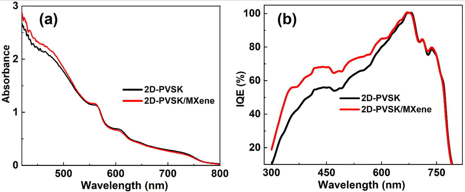 | ||
| Fig. 5 (a) Stationary absorption spectra and (b) internal quantum efficiency for pristine and MXene-passivated PSC. | ||
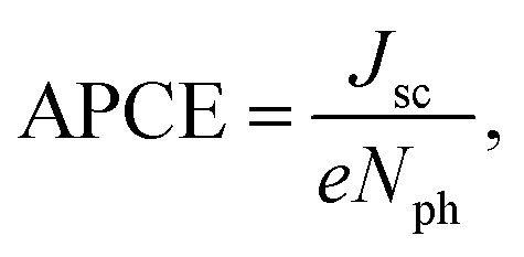
To obtain more information about the total number of absorbed photons that participated in the current generation, the number of photons (Nph) was calculated from the stationary absorption spectra, and used in eqn (1) to determine the total absorbed photon to current efficiency (APCE). In specific, the total APCE describes the relative photocurrent of the cells per the number of absorbed photons:58
 | (1) |
Similarly, external quantum efficiency (EQE) data have been used to re-confirm the total APCE. EQE spectra were measured and also an integrated current density was determined from the I–V measurement as shown in Fig. S6, ESI.† The MXene-passivated device shows a significant enhancement in the spectral response over the entire EQE curves compared with that of the pristine device. The internal quantum efficiency (IQE) has been calculated with the help of EQE using eqn (2), which explains the charge collection efficiency.
 | (2) |
One can observe from Fig. 5b that the IQE spectra of the MXene-based device exhibited better charge collection efficiency than the pristine device, which leads to the enhanced current density of the PSC. The IQE is closely 100% near the 700 nm wavelength, which might be attributed to more absorption by the bulk phase. However, the quasi-2D phases (below 650 nm) contribute to smaller charge collection efficiency (50–70% in the range of 400–600 nm). Thus, losses due to insufficient charge collection from low dimensional perovskite species are another source of low JSC. The average value of IEQ is very close to that of the total APCE calculated with and without MXene-based PSCs.
3.4. Air and photostability of the PSC
It is important to fabricate a stable device for commercialization. The fabricated device is based on 2D perovskite and 2D MXene. Since 2D perovskite is quite stable compared to bulk perovskite, here we are expecting to improve the device stability even more after adding a layer of MXene as a hole interfacial layer. To confirm this, we have performed air stability measurements for both samples, i.e., with and without MXene-based PSC. The device fabrication and measurement were performed under the dry-air atmosphere, and further, unsealed PSCs in open-air conditions were kept for over 50 days. Meanwhile, the performance was measured after an interval of 10 days systematically. The air stability results are shown in Fig. 6a, which depicts the remarkable stability of MXene-passivated devices. In the early days, MXene-based devices slightly improved the PCE which might be induced by the reduction of many defects with aging.59 Afterward, the PCE of the device reduced very slowly and delivered a similar performance even after 1250 h of aging in open-air conditions as on the first day. The MXene as a passivation/interfacial layer (∼50 nm, Fig. S5, ESI†) on the 2D perovskite, protects from the moisture and air available in the atmosphere, leading to a slow reduction in the device's performance. In contrast, almost 20% PCE reduction can be observed in the reference device after exposing it to open air for 1250 h. Furthermore, we also checked the air stability of both devices, which have been kept in dry air for six months. Interestingly, MXene based device demonstrated around 95% stability (Fig. S1 and Table S1, ESI†).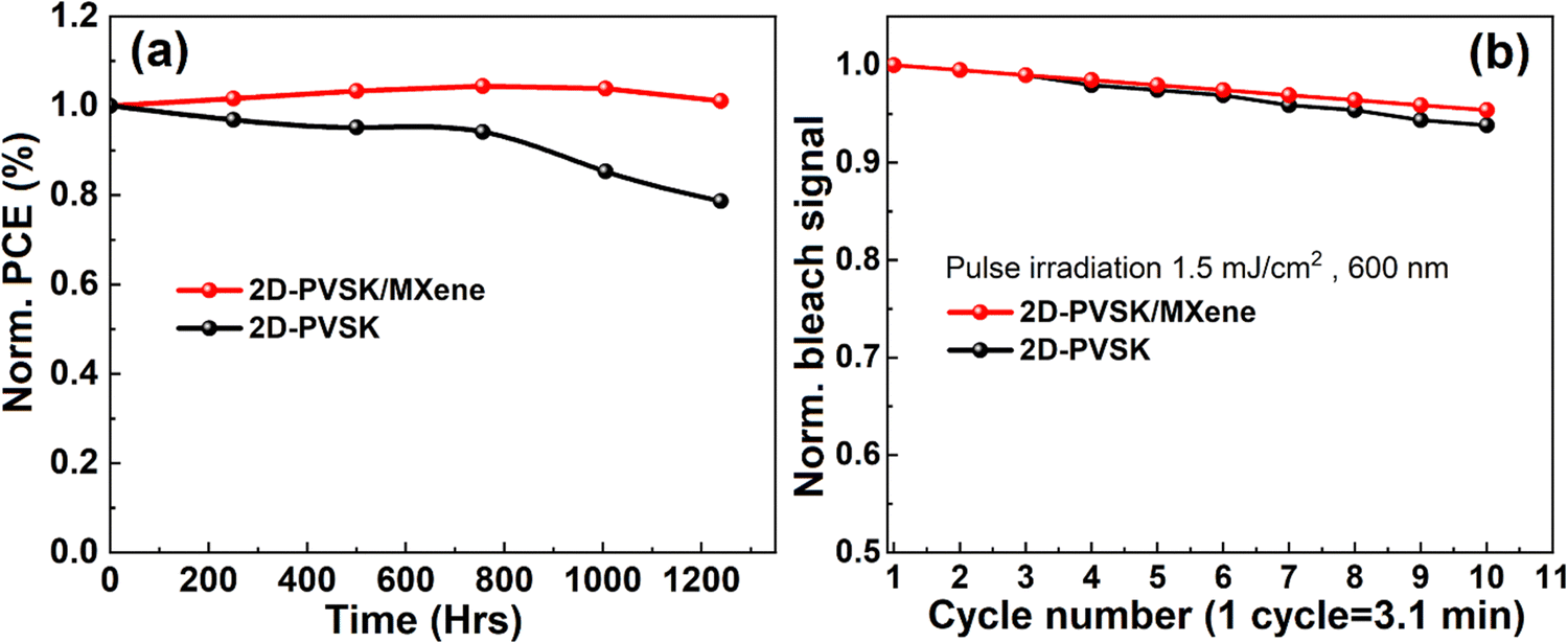 | ||
| Fig. 6 (a) Stability of the PCE under open-air conditions and (b) photostability under fs pulse excitation for pristine and MXene-passivated PSC. The pump pulse was 1.5 mJ cm−2 at 600 nm, and TA amplitude at 712 nm and fixed time delay at 6 ps after excitation (maximum of the bulk bleach signal) is taken to monitor the photodegradation. | ||
Similarly, we have also monitored the photoinduced degradation of perovskite samples under strong pump pulse fluence using a TA setup. A decrease in the amplitude of the initial bulk phase bleach (see the next paragraph for details) at a fixed time delay was taken as the measure of photostability. Fig. 6b presents the results for strong irradiation at 600 nm with a pump fluence of 1.5 mJ cm−2 for 30 min. As can be seen, the bleach amplitude for both the samples with and without MXene decreases only by about 5%. A small effect of the MXene layer has been observed in the reduction of photodegradation. From the point of view of the number of absorbed photons, such pulse excitation corresponds to the irradiation of 17 suns, so the stability of the samples is quite remarkable. However, the excitation at 475 nm (at the same fluence of 1.5 mJ cm−2 corresponding to the same number of absorbed photons as at 600 nm) results in much faster degradation – bleach amplitude decreases by about 30% during the same time (Fig. S7, ESI†). A decrease of about 10% is already observed when the pump fluence at 475 nm is lowered to 125 μJ cm−2. The difference might originate from a shorter penetration depth at 475 nm than at 600 nm (about 4 times, resulting in different initial carrier concentrations) and/or a higher population of low dimensional phases at 475 nm.
3.5. Transient absorption
TA measurements reveal the distribution of the low-dimensional phases and the dynamics of the charge decay in fabricated PSCs. TA also enabled us to probe the cells from the two sides: TiO2 (ETL) and Spiro-OMeTAD (HTL) due to short-wavelength excitation at 475 nm. High absorbance (>2) of the perovskite layer at this wavelength results in a short penetration depth of several tens of nm. Fig. S8a–d (ESI†) shows the exemplary TA results in pseudo-3D colour plots. TA spectra and their temporal evolution have been discussed earlier for this and similar RP quasi-2D perovskites in inverted structures,41,55,56,60,61 and those previous findings are mostly relevant to our current study. The bulk phase is recognized as an intense negative bleach peak at the stationary absorption edge (∼740 nm) which appears due to the band filling mechanism.62,63 In the shorter wavelength range (<700 nm) the positive TA signal is interrupted by several negative bleaches of low dimensional phases which have higher bandgaps than that of the bulk phase. The most visible phases are related to n = 2 (peak ∼565 nm), n = 3 (610 nm), and n = 4 (645 nm), where n indicates the number of stacked 2D layers separated by big 4F-PEA cations in this mixed quasi-2D structure.56 The decay of low-dimensional phases is faster than the decay of the bulk phase and, at least partially, the charges are transferred from low-n phases to the bulk phase.60,61The presented TA analysis is based on a global fit with 3-exponential components. The exemplary wavelength-dependent amplitudes of different time components are shown in Fig. 7, and the fit quality is presented in Fig. S9 (ESI†). In general, the evolution of almost all processes occurring in perovskites after ultrafast excitation cannot be described simply by exponential functions.64 However, our simplified multi-exponential approach gives the average lifetimes which analyzing their associated spectral changes, can be assigned to different processes, and then these average lifetimes can be compared for the samples with and without MXenes. The fastest component (τ1 < 1 ps) describes the charge cooling process (negative amplitudes in 670–730 nm and positive amplitudes in 730–800 nm spectral ranges in Fig. 7)65 and the initial decay of low phase components (negative amplitudes of the bleaches from 550 to 650 nm).41 The second component (τ2) is mainly due to further decay of low-n bleaches (negative peaks in 550–650 nm range) and partial rise of the bulk phase bleach (positive amplitude ∼750 nm). The third component (τ3) mainly shows the decay of the bulk phase (negative amplitudes of the bleach between 700 and 800 nm) that appears due to charge recombination and charge extraction (injection) to contact materials.58
 | ||
| Fig. 7 Wavelength-dependant amplitudes of the indicated time constants from a 3-exponential global fit of TA data excited from HTL side at 475 nm with 2.5 μJ cm−2 pump fluence for the cells: (a) without MXene and (b) with MXene. | ||
First, our TA analysis was used to compare the distribution of low-n phases in the samples with and without MXenes. Table 1 presents the relative population of these phases with respect to the bulk phase based on the TA amplitude ratios at the corresponding minima. The amplitudes of n = 2, 3, and 4 phases were taken just after excitation (from the sum of the amplitudes of all global fit components with the subtraction of positive TA background signal), while the amplitude of the bulk phase was taken after the initial charge cooling when the bulk bleach band at the absorption edge appears (from the sum of all amplitudes excluding that of the fastest component – τ1). It can be observed that at the glass (ETL) side, the amplitude ratios of the low-n/bulk phase are similar for 2D-PVSK/MXene and the reference 2D-PVSK cells. However, for the excitation from the HTL side about 30% less low dimensional phases are found for the samples with MXene with respect to those without MXene (Table 1). It indicates that in the process of quasi-2D perovskite formation, slightly less low dimensional phases are formed close to the HTL when MXene is present. It is possible because MXene is dispersed in the anti-solvent mixture, which can probably influence the crystallization close to the upper interface. Most probably, the reduced population of low-n phases enhances the charge (hole) extraction to HTL since this TA result can be correlated with the EQE and IQE spectra (Fig. 5b and Fig. S6, ESI†). In the short wavelength range (<600 nm) where low-n phases are present the efficiency of photon-to-current conversion is slightly higher for the cells with than without MXene.
| Sample | Excitation side | n = 2/bulk | n = 3/bulk | n = 4/bulk |
|---|---|---|---|---|
| 2D-PVSK | ETL (glass) | 1.2 | 0.78 | 0.22 |
| 2D-PVSK/MXene | ETL (glass) | 1.5 | 0.84 | 0.21 |
| 2D-PVSK | HTL | 0.83 | 0.64 | 0.19 |
| 2D-PVSK/MXene | HTL | 0.63 | 0.43 | 0.13 |
Next, our TA global analysis was used to compare the possible effect of MXene layers on the dynamics of different charge transfer and recombination processes. Table 2 collects the time constants of different components for the excitation from the HTM side at different pump pulse fluences. In almost all cases the first two components (τ1 and τ2) are slightly longer for the samples with MXenes than for the reference cells. It can suggest that the decay of the low-n phase population is slowed down in the presence of MXenes. However, it is difficult to say if it is due to the interaction with MXenes itself or due to the smaller population of low-n phases close to the MXene layer revealed above. In contrast, the lifetimes of the third component (τ3, related to the bulk phase decay) are within the experimental error, the same for the samples with and without the MXene (Table 2). This decay at high pump fluence (25 μJ cm−2) reflects mainly the effect of second-order (radiative) recombination, while at low pump fluence (1 μJ cm−2 and 2.5 μJ cm−2) – also the contribution of charge extraction to contact materials (hole injection processes in this case).66 It indicates that both the above processes (rate constants of recombination and hole extraction from the bulk phase to HTM) are not affected by the presence of MXene.
| Sample | Pump fluence | τ 1, fs | τ 2, ps | τ 3, ns |
|---|---|---|---|---|
| 2D-PVSK | 1 μJ cm−2 | 235 | 150 | 14.1 |
| 2D-PVSK/MXene | 210 | 155 | 15.6 | |
| 2D-PVSK | 2.5 μJ cm−2 | 355 | 145 | 5.8 |
| 2D-PVSK/MXene | 375 | 205 | 5.6 | |
| 2D-PVSK | 25 μJ cm−2 | 530 | 33 | 1.55 |
| 2D-PVSK/MXene | 555 | 35 | 1.55 | |
| 2D-PVSK | 125 μJ cm−2 | 690 | 26 | 1.10 |
| 2D-PVSK/MXene | 695 | 29 | 1.12 |
Finally, we have also checked if TA signals of MXene layers can have any possible effects on the observed TA dynamics and spectra of our PSCs. Thus, we performed TA measurements for the samples with only MXene layers on FTO, deposited either by spin-coating (like in PSC) or drop-casting (less uniform but a thicker MXene layer, Fig. S10, ESI†). Pseudo-3D colour plots of TA data are shown in Fig. S8e and f (ESI†). It can be seen that the amplitude of the TA signal is 3–4 times smaller for the spin-coating sample than the drop-cast one, and in both cases, the positive TA features below 700 nm and negative amplitudes above 700 nm can be detected. Fig. S10 (ESI†) shows the results of a 3-exponential global analysis of TA of the MXene layer, which is in agreement with the previous report of TA studies for the same Mxene.67 The ultrafast component (∼100 fs) can be assigned to electron–electron scattering and electron–phonon coupling, while the longer component (∼15 ps) and the constant offset component (>20 ns, taking into account the temporal 3 ns window of our setup) possess the characteristic features of absorption band shift and are due to faster and slower thermalization processes. To be able to detect a reasonable TA signal (higher than the noise) the pump fluence at 475 nm had to be increased to 600 μJ cm−2. Thus, taking into account that TA signal of MXenes has been observed to scale linearly with pump fluence,67 we can estimate that MXene excitation contribution during the measurements of our PSC samples is ∼360 times smaller in the positive amplitudes part and ∼840 times smaller in the negative part of the perovskite TA signals, so it cannot have any effect on the analyzed data of PSC (lifetimes and low-n phases population).
4. Conclusions
In summary, we have synthesized a Ti3C2Tx MXene, and successfully employed it as a passivation/interfacial layer between the 2D-perovskite and the HTL in the regular structure of PSCs. The PSC with MXene has demonstrated more than 9% enhancement in the performance as compared to the reference device. The MXene served here as a conducting bridge for holes to transfer from the perovskite to the HTL and contributed to increasing the overall performance of the device. Moreover, MXene passivation has improved the stability significantly, where, even after 50 days, the device demonstrated only >1% reduction in terms of performance under an open-air atmosphere. Overall, the MXene has worked in several different ways in the PSCs. The first is to adjust the energy alignment which might provide reliable pathways for the positive charge transfer. Second, is the passivator for the perovskite film, which can reduce the traps/defects, and subsequently reduce the non-radiative recombination loss in the device. Thirdly, the MXene layer acts as a barrier that protects perovskite from moisture and air in the outer atmosphere. Lastly, transient absorption results indicate a slightly smaller concentration of low-dimensional phases and their slightly longer lifetime close to the HTL when the MXene is applied. However, the successful integration of MXene as an HTL interfacial layer in PSCs involves many challenges including optimizing the solution concentration, a solid interface between the MXene layer and 2D perovskite, and ensuring compatibility with other components of the device.Conflicts of interest
There are no conflicts of interest to declare.Acknowledgements
Sanjay Sahare thanks project No. 2021/43/P/ST3/02599 co-funded by the National Science Centre and the European Union's Horizon 2020 research and innovation program under the Marie Skłodowska–Curie grant agreement no. 945339. Mykhailo Solovan thanks the Polish National Agency for Academic Exchange (NAWA) for financial support within the Ulam NAWA Program (No. BPN/ULM/2021/1/00230). Marina Smirnova was financially supported by the National Science Centre under the Preludium 3 Bis project (UMO-2021/43/O/ST5/00137). Dr Patryk Florczak from the NanoBioMedical Centre, AMU, is kindly acknowledged for the maintenance of the chemical lab. Dr Mateusz Gierszewski from the Faculty of Physics, AMU is acknowledged for his help in stationary photoluminescence measurements.References
- J. Park, J. Kim, H. S. Yun, M. J. Paik, E. Noh, H. J. Mun, M. G. Kim, T. J. Shin and S. Il Seok, Nature, 2023, 616, 724–730 CrossRef CAS PubMed.
- T. Ozturk, E. Akman, A. E. Shalan and S. Akin, Nano Energy, 2021, 87, 106157 CrossRef CAS.
- N. Rolston, A. D. Printz, J. M. Tracy, H. C. Weerasinghe, D. Vak, L. J. Haur, A. Priyadarshi, N. Mathews, D. J. Slotcavage, M. D. McGehee, R. E. Kalan, K. Zielinski, R. L. Grimm, H. Tsai, W. Nie, A. D. Mohite, S. Gholipour, M. Saliba, M. Grätzel and R. H. Dauskardt, Adv. Energy Mater., 2018, 8, 1702116 CrossRef.
- Y. Bai, X. Meng and S. Yang, Adv. Energy Mater., 2018, 8, 1701883 CrossRef.
- S. Sahare, H. D. Pham, D. Angmo, P. Ghoderao, J. MacLeod, S. B. Khan, S. L. Lee, S. P. Singh and P. Sonar, Adv. Energy Mater., 2021, 11, 2101085 CrossRef CAS.
- R. D. Chavan, B. Bończak, J. Kruszyńska, A. Mahapatra, M. Ans, J. Nawrocki, K. Nikiforow, P. Yadav, J. Paczesny, F. Sadegh, M. Unal, S. Akin and D. Prochowicz, Chem. Mater., 2023, 35, 8309–8320 CrossRef CAS.
- N. Yukta, R. D. Chavan, A. Mahapatra, D. Prochowicz, P. Yadav, P. K. Iyer and S. Satapathi, ACS Appl. Mater. Interfaces, 2023, 15, 53351–53361 CrossRef PubMed.
- H. Zhang, M. K. Nazeeruddin and W. C. H. Choy, Adv. Mater., 2019, 31, 1805702 CrossRef PubMed.
- Y. R. Shi, K. L. Wang, Y. H. Lou, G. L. Liu, C. H. Chen, J. Chen, L. Zhang and Z. K. Wang, Adv. Mater., 2022, 34, 2205338 CrossRef CAS PubMed.
- J. Li, R. Xia, W. Qi, X. Zhou, J. Cheng, Y. Chen, G. Hou, Y. Ding, Y. Li, Y. Zhao and X. Zhang, J. Power Sources, 2021, 485, 229313 CrossRef CAS.
- F. Matteocci, L. Cinà, E. Lamanna, S. Cacovich, G. Divitini, P. A. Midgley, C. Ducati and A. Di Carlo, Nano Energy, 2016, 30, 162–172 CrossRef CAS.
- J. Zhu, B. He, M. Wang, X. Yao, H. Huang, C. Chen, H. Chen, Y. Duan and Q. Tang, Nano Energy, 2022, 104, 107920 CrossRef CAS.
- C. Das, R. Roy, M. Kedia, M. Kot, W. Zuo, R. Félix, T. Sobol, J. I. Flege and M. Saliba, ACS Appl. Mater. Interfaces, 2023, 15, 56500–56510 CrossRef CAS PubMed.
- C. Zhi, Z. Li and B. Wei, APL Mater., 2021, 9, 70702 CrossRef CAS.
- Y. Xu, M. Wang, Y. Lei, Z. Ci and Z. Jin, Adv. Energy Mater., 2020, 10, 2002558 CrossRef CAS.
- A. Caiazzo, R. A. J. Janssen, A. Caiazzo and R. A. J. Janssen, Adv. Energy Mater., 2022, 12, 2202830 CrossRef CAS.
- H. Tsai, W. Nie, J. C. Blancon, C. C. Stoumpos, R. Asadpour, B. Harutyunyan, A. J. Neukirch, R. Verduzco, J. J. Crochet, S. Tretiak, L. Pedesseau, J. Even, M. A. Alam, G. Gupta, J. Lou, P. M. Ajayan, M. J. Bedzyk, M. G. Kanatzidis and A. D. Mohite, Nature, 2016, 536, 312–316 CrossRef CAS PubMed.
- J. W. Lee, Z. Dai, T. H. Han, C. Choi, S. Y. Chang, S. J. Lee, N. De Marco, H. Zhao, P. Sun, Y. Huang and Y. Yang, Nat. Commun., 2018, 9, 1–10 CrossRef PubMed.
- S. Wang, T. Sakurai, W. Wen and Y. Qi, Adv. Mater. Interfaces, 2018, 5, 1800260 CrossRef.
- A. Fakharuddin, L. Schmidt-Mende, G. Garcia-Belmonte, R. Jose and I. Mora-Sero, Adv. Energy Mater., 2017, 7, 1700623 CrossRef.
- M. I. Saidaminov, J. Kim, A. Jain, R. Quintero-Bermudez, H. Tan, G. Long, F. Tan, A. Johnston, Y. Zhao, O. Voznyy and E. H. Sargent, Nat. Energy, 2018, 3, 648–654 CrossRef CAS.
- I. Lee, J. H. Yun, H. J. Son and T. S. Kim, ACS Appl. Mater. Interfaces, 2017, 9, 7029–7035 CrossRef CAS PubMed.
- Q. Van Le, J. Y. Choi and S. Y. Kim, FlatChem, 2017, 2, 54–66 CrossRef CAS.
- X. Zhao, S. Liu, H. Zhang, S. Y. Chang, W. Huang, B. Zhu, Y. Shen, C. Shen, D. Wang, Y. Yang and M. Wang, Adv. Funct. Mater., 2019, 29, 1805168 CrossRef.
- M. Acik and S. B. Darling, J. Mater. Chem. A, 2016, 4, 6185–6235 RSC.
- L. Yang, D. Kan, C. Dall’Agnese, Y. Dall’Agnese, B. Wang, A. K. Jena, Y. Wei, G. Chen, X. F. Wang, Y. Gogotsi and T. Miyasaka, J. Mater. Chem. A, 2021, 9, 5016–5025 RSC.
- C. Long, K. Huang, J. Chang, C. Zuo, Y. Gao, X. Luo, B. Liu, H. Xie, Z. Chen, J. He, H. Huang, Y. Gao, L. Ding and J. Yang, Small, 2021, 17, 2102368 CrossRef CAS PubMed.
- S. Sahare, P. Ghoderao, P. Yin, A. S. Saleemi, S. L. Lee, Y. Chan and H. Zhang, Small Methods, 2022, 6, 2101599 CrossRef CAS PubMed.
- N. H. Solangi, S. A. Mazari, N. M. Mubarak, R. R. Karri, N. Rajamohan and D. V. N. Vo, Environ. Res., 2023, 222, 115337 CrossRef CAS PubMed.
- X. Li, Z. Huang, C. E. Shuck, G. Liang, Y. Gogotsi and C. Zhi, Nat. Rev. Chem., 2022, 6, 389–404 CrossRef PubMed.
- K. Hantanasirisakul and Y. Gogotsi, Adv. Mater., 2018, 30, 1804779 CrossRef PubMed.
- A. Agresti, A. Pazniak, S. Pescetelli, A. Di Vito, D. Rossi, A. Pecchia, M. Auf der Maur, A. Liedl, R. Larciprete, D. V. Kuznetsov, D. Saranin and A. Di Carlo, Nat. Mater., 2019, 18, 1228–1234 CrossRef CAS PubMed.
- Y. Li, D. Wang, L. Yang and S. Yin, J. Alloys Compd., 2022, 904, 163742 CrossRef CAS.
- Z. Guo, L. Gao, Z. Xu, S. Teo, C. Zhang, Y. Kamata, S. Hayase and T. Ma, Small, 2018, 14, 1802738 CrossRef PubMed.
- S. Qamar, K. Fatima, N. Ullah, Z. Akhter, A. Waseem and M. Sultan, Nanoscale, 2022, 14, 13018–13039 RSC.
- X. Jin, L. Yang and X. F. Wang, Nano-Micro Lett., 2021, 13, 1–13 CAS.
- S. Palei, G. Murali, C. H. Kim, I. In, S. Y. Lee and S. J. Park, Nano-Micro Lett., 2023, 15, 1–39 Search PubMed.
- L. Yang, P. Hou, B. Wang, C. Dall’Agnese, Y. Dall’Agnese, G. Chen, Y. Gogotsi, X. Meng and X. F. Wang, Chem. Eng. J., 2022, 446, 136963 CrossRef CAS.
- J. Zhang, C. Huang and H. Yu, Appl. Phys. Lett., 2021, 19(3), 033506 CrossRef.
- J. Zhang, C. Huang, Y. Sun and H. Yu, Adv. Funct. Mater., 2022, 32, 2113367 CrossRef CAS.
- S. Sahayaraj, E. Radicchi, M. Ziółek, M. Ścigaj, M. Tamulewicz-Szwajkowska, J. Serafińczuk, F. De Angelis and K. Wojciechowski, J. Mater. Chem. A, 2021, 9, 9175–9190 RSC.
- B. Scheibe, J. K. Wychowaniec, M. Scheibe, B. Peplińska, M. Jarek, G. Nowaczyk and Ł. Przysiecka, ACS Biomater. Sci. Eng., 2019, 5, 6557–6569 CrossRef CAS PubMed.
- Q. Jiang, Y. Zhao, X. Zhang, X. Yang, Y. Chen, Z. Chu, Q. Ye, X. Li, Z. Yin and J. You, Nat. Photonics, 2019, 13, 460–466 CrossRef CAS.
- S. Abicho, B. Hailegnaw, G. A. Workneh and T. Yohannes, Mater. Renew. Sustain. Energy, 2021, 11, 47–70 CrossRef.
- M. Shao, T. Bie, L. Yang, Y. Gao, X. Jin, F. He, N. Zheng, Y. Yu and X. Zhang, Adv. Mater., 2022, 34, 2107211 CrossRef CAS PubMed.
- T. B. Limbu, B. Chitara, M. Y. Garcia Cervantes, Y. Zhou, S. Huang, Y. Tang and F. Yan, J. Phys. Chem. C, 2020, 124, 17772–17782 CrossRef CAS.
- L. Yang, D. Kan, C. Dall’Agnese, Y. Dall’Agnese, B. Wang, A. K. Jena, Y. Wei, G. Chen, X. F. Wang, Y. Gogotsi and T. Miyasaka, J. Mater. Chem. A, 2021, 9, 5016–5025 RSC.
- Y. Huang, Y. Li, E. L. Lim, T. Kong, Y. Zhang, J. Song, A. Hagfeldt and D. Bi, J. Am. Chem. Soc., 2021, 143, 3911–3917 CrossRef CAS PubMed.
- M. Minbashi and E. Yazdani, Phys. Chem. Chem. Phys., 2023, 25, 5146–5155 RSC.
- E. H. Balaguera and J. Bisquert, ACS Energy Lett., 2024, 9, 478–486 CrossRef PubMed.
- D. H. Kang and N. G. Park, Adv. Mater., 2019, 31, 1805214 CrossRef PubMed.
- H. P. Parkhomenko, M. M. Solovan, S. Sahare, A. I. Mostovyi, D. Aidarkhanov, N. Schopp, T. Kovaliuk, M. Kaikanov, A. Ng and V. V. Brus, Adv. Funct. Mater., 2023, 2310404 Search PubMed.
- H. P. Parkhomenko, Y. Yerlanuly, V. V. Brus and A. N. Jumabekov, Org. Electron., 2024, 129, 107049 CrossRef CAS.
- V. V. Brus, C. M. Proctor, N. A. Ran and T. Q. Nguyen, Adv. Energy Mater., 2016, 6, 1502250 CrossRef.
- B. Wilk, S. Sahayaraj, M. Ziółek, V. Babu, R. Kudrawiec and K. Wojciechowski, Adv. Mater. Technol., 2022, 7, 2200606 CrossRef CAS.
- F. Zheng, C. Zuo, M. Niu, C. Zhou, S. J. Bradley, C. R. Hall, W. Xu, X. Wen, X. Hao, M. Gao, T. A. Smith and K. P. Ghiggino, ACS Appl. Mater. Interfaces, 2020, 12, 25980–25990 CrossRef CAS PubMed.
- Y. Lin, Y. Bai, Y. Fang, Z. Chen, S. Yang, X. Zheng, S. Tang, Y. Liu, J. Zhao and J. Huang, J. Phys. Chem. Lett., 2018, 9, 654–658 CrossRef CAS PubMed.
- K. Pydzińska-Białek, V. Drushliak, E. Coy, K. Zaleski, J. Flach, J. Idígoras, L. Contreras-Bernal, A. Hagfeldt, J. A. Anta and M. Ziółek, ACS Appl. Mater. Interfaces, 2020, 12, 30399–30410 CrossRef PubMed.
- Y. Han, S. Meyer, Y. Dkhissi, K. Weber, J. M. Pringle, U. Bach, L. Spiccia and Y. B. Cheng, J. Mater. Chem. A, 2015, 3, 8139–8147 RSC.
- L. N. Quan, Y. Zhao, F. P. García De Arquer, R. Sabatini, G. Walters, O. Voznyy, R. Comin, Y. Li, J. Z. Fan, H. Tan, J. Pan, M. Yuan, O. M. Bakr, Z. Lu, D. H. Kim and E. H. Sargent, Nano Lett., 2017, 17, 3701–3709 CrossRef CAS PubMed.
- A. Fakharuddin, M. Franckevičius, A. Devižis, A. Gelžinis, J. Chmeliov, P. Heremans and V. Gulbinas, Adv. Funct. Mater., 2021, 31, 2010076 CrossRef CAS.
- T. C. Sum, N. Mathews, G. Xing, S. S. Lim, W. K. Chong, D. Giovanni and H. A. Dewi, Acc. Chem. Res., 2016, 49, 294–302 CrossRef CAS PubMed.
- J. S. Manser and P. V. Kamat, Nat. Photonics, 2014, 8, 737–743 CrossRef CAS.
- K. Pydzińska-Białek, J. Szeremeta, K. Wojciechowski and M. Ziółek, J. Phys. Chem. C, 2019, 123, 110–119 CrossRef.
- M. T. Trinh, X. Wu, D. Niesner and X. Y. Zhu, J. Mater. Chem. A, 2015, 3, 9285–9290 RSC.
- K. Szulc, K. Pydzińska-Białek and M. Ziółek, Materials, 2023, 16, 7110 CrossRef CAS PubMed.
- Q. Zhang, L. Yan, M. Yang, G. Wu, M. Hu, J. Li, K. Yuan and X. Yang, ACS Appl. Mater. Interfaces, 2020, 124, 30 Search PubMed.
Footnotes |
| † Electronic supplementary information (ESI) available. See DOI: https://doi.org/10.1039/d4tc00466c |
| ‡ Authors share equal contribution. |
| This journal is © The Royal Society of Chemistry 2024 |