
 Open Access Article
 This Open Access Article is licensed under a
 Creative Commons Attribution 3.0 Unported Licence
Electrochemical rewiring through quantum conductance effects in single metallic memristive nanowires†
Gianluca
Milano
 *a,
Federico
Raffone
*b,
Katarzyna
Bejtka
bc,
Ivan
De Carlo
ad,
Matteo
Fretto
a,
Fabrizio Candido
Pirri
bc,
Giancarlo
Cicero
b,
Carlo
Ricciardi
b and
Ilia
Valov
ef
*a,
Federico
Raffone
*b,
Katarzyna
Bejtka
bc,
Ivan
De Carlo
ad,
Matteo
Fretto
a,
Fabrizio Candido
Pirri
bc,
Giancarlo
Cicero
b,
Carlo
Ricciardi
b and
Ilia
Valov
ef
aAdvanced Materials Metrology and Life Sciences Division, INRiM (Istituto Nazionale di Ricerca Metrologica), Strada delle Cacce 91, 10135 Torino, Italy. E-mail: g.milano@inrim.it
bDepartment of Applied Science and Technology, Politecnico di Torino, C.so Duca degli Abruzzi 24, 10129 Torino, Italy. E-mail: federico.raffone@polito.it
cCentre for Sustainable Future Technologies, Istituto Italiano di Tecnologia, Via Livorno 60, 10144 Torino, Italy
dDepartment of Electronics and Telecommunications, Politecnico di Torino, C.so Duca degli Abruzzi 24, 10129 Torino, Italy
eForschungszentrum Jülich, Institute of Electrochemistry and Energy System, WilhelmJohnen-Straße, 52428, Jülich, Germany
f“Acad. Evgeni Budevski” (IEE-BAS), Bulgarian Academy of Sciences (BAS), Acad. G. Bonchev Str., Block 10, 1113 Sofia, Bulgaria
First published on 9th January 2024
Abstract
Memristive devices have been demonstrated to exhibit quantum conductance effects at room temperature. In these devices, a detailed understanding of the relationship between electrochemical processes and ionic dynamic underlying the formation of atomic-sized conductive filaments and corresponding electronic transport properties in the quantum regime still represents a challenge. In this work, we report on quantum conductance effects in single memristive Ag nanowires (NWs) through a combined experimental and simulation approach that combines advanced classical molecular dynamics (MD) algorithms and quantum transport simulations (DFT). This approach provides new insights on quantum conductance effects in memristive devices by unravelling the intrinsic relationship between electronic transport and atomic dynamic reconfiguration of the nanofilment, by shedding light on deviations from integer multiples of the fundamental quantum of conductance depending on peculiar dynamic trajectories of nanofilament reconfiguration and on conductance fluctuations relying on atomic rearrangement due to thermal fluctuations.
New conceptsQuantum conductance effects in memristive devices play a crucial role in determining transport properties when approaching ultimate device scaling down to the near atomic scale. Here, we analyze experimentally and computationally the dynamic correlation between filament morphology, electronic transport properties and quantum conductance effects. For the study, a new computational approach was developed to combine reactive classical molecular dynamics and quantum transport simulations able to properly capture both the dynamic evolution of the electrochemical formation of conductive filaments in memristive devices and associated quantum conductance. In accordance with experimental results, this approach allowed us to investigate (i) the relationship between observed deviations of conductance levels from integer multiples of the fundamental quantum of conductance and peculiar dynamic trajectories of filament atomic reconfiguration and (ii) conductance fluctuations arising from atomic reconfiguration near the quantum point contacts related to thermal fluctuations. |
Introduction
Quantum conductance effects in memristive devices represent a potential breakthrough for the development of new device concepts and information processing technologies based on quantum phenomena. Coupling ionics with electronics, redox-based memristive devices are two terminal nanoionic devices where functionalities rely on the electrochemical formation/rupture of nanosized filaments under the action of the applied electric field with consequent variation of the internal state of resistance.1–4 When the width of the conductive filament becomes comparable with the elastic mean free path of electrons, electronic transport undergoes a diffusive to ballistic crossover. Under these circumstances, the conductive filament forms a quantum point contact (QPC), i.e., a narrow constriction connecting two electrically conductive regions, where conductance is quantized in terms of the fundamental unit of conductance G0 as explained by the Landauer theory.5–7 While in semiconductor devices the QPC can be considered a mesoscopic object due to the large Fermi wavelength and can be observed only at cryogenic temperatures, in metallic filaments QPC are characterized by atomic dimensions since the Fermi wavelength is of the same order of magnitude as the atomic separation and can be observed at room temperature. In this context, quantum effects have been reported in a wide range of redox-based memristive cells realized with a top-down approach,5,8–15 The quantum conductance regime in memristive devices, that can be observed when the internal resistance state approaches the range of few conductance quanta (i.e., in the ∼3 to 15 kΩ range), has been demonstrated to be related to the formation of truly atomic-sized metallic filments.6 In this context, quantum conductance effects cannot be neglected when approaching the ultimate device scaling down to the near atomic scale. While on one side quantum conductance effects have been associated with state fluctuations and enlarged noise due to atomic instabilities at the quantum point contact,16 on the other side these effects can be exploited for new device concepts for multilevel data storage, logics, signal processing, quantum metrology and neuromorphic computing.5In this work, we report on quantum conductance effects in single memristive NWs through a combined experimental and simulation approach. It is shown that Ag NWs, that are initially highly conductive, exhibit resistive switching behavior after electrically induced breakdown events that cause the formation of a needle-like nanogap along the wire, as investigated by in situ STEM measurements. Electrochemical rewiring/rupture of the NW is responsible for resistive switching phenomena, where the electrically driven reconfiguration of the nanofilament atomic structure results in quantum conductance effects, as revealed by the presence of peaks at multiples of G0 in conductance histograms. A new computational approach is introduced by combining advanced classical molecular dynamics algorithms with quantum transport simulations. Such an approach takes advantage of both simulation techniques to accurately describe electrochemical phenomena and ionic dynamics that shape the morphology of the nanofilament across the nanogap, while, at the same time, monitoring the ballistic electronic conduction of the NW. This allows a complete description of the electrochemical rewiring process of a memristive device from the atomistic point of view. In accordance with experimental results, simulations, performed by analyzing the realistic dynamic evolution of the atomic configuration of the nanofilament through molecular dynamics (MD) while determining its electronic transport properties through Density Functional Theory (DFT), show that the peculiar arrangement of atoms near the QPC depends on the dynamic evolution of nanofilament reconfiguration that gives rise to deviations of conductance values from integer multiples of G0. Furthermore, simulations show that experimental fluctuations over time in the nanofilament conductance around multiples of G0 can be ascribed to thermal fluctuations leading to atomic reconfigurations near the QPC. By exploiting the single Ag NW as a model system, these results provide insights on the relationship between quantum phenomena and dynamics of atomic reconfiguration of atomic-sized filaments in resistive switching devices.
Results and discussions
Memristive devices based on single Ag NWs have been realized by contacting Ag NWs dispersed on an insulating substrate with a pre-patterned submillimeter probe circuit through Pt contacts (Fig. 1a, Methods). Oppositely to conventional memristive devices, single Ag NW memristive devices exhibit a low pristine state resistance (Fig. S1 and Table S1, ESI†). The device resistance can be turned from a low resistance state to a high resistance state by electrical induced breakdown events related to Joule heating and electromigration phenomena occurring at high current densities that drive the formation of a needle-like nanogap across the NW.17–20Fig. 1b reports breakdown events in different single NW-based devices induced by voltage sweep stimulation, together with a schematization of the electrical circuital representations of the device before and after breakdown. Despite variability in the breakdown voltage, all NWs show a sudden decrease of flowing current due to electrical breakdown. Before breakdown (i.e., in the pristine state), the low resistance state relies on the NW resistance RNW and on the resistance at the Pt–Ag NW interface R* (Rpristine ≈ 2R* + RNW). After breakdown, instead, the NW device resistance can be expressed as R ≈ 2RC + RNWa + Rgap + RNWb, where RNWaand RNWb represent the resistance of the two NW disconnected parts (where RNWa + RNWb ≈ RNW) while Rgap is the nanogap resistance. In this context, it is worth noticing that this device configuration allows to estimate the gap resistance Rgap by subtracting the effect of R* and RNW parasitic resistances (Note S1, ESI†). As an example, the morphology of an electrically induced nanogap in an Ag NW is reported in Fig. 1c. A detailed investigation of NW breakdown was performed by means of in situ STEM measurements (methods, details in Fig. S2, ESI†). By exploiting this technique, it is possible to correlate the electrical response of the NW (Fig. 1d) with the evolution of its morphology (Fig. 1e and Movie S1, ESI†). As can be observed, an increase of the applied voltage corresponds to a thinning of the NW (timeframe 1,2 and 3, Fig. 1e) due to migration of metal ions and accumulation of depleted ions at the anode side as detailed in Movie S1 (ESI†). A further increase of the applied voltage results in a sudden decrease of the current that results from the breaking of the Ag NW (timeframe 4, Fig. 1f). In this context, results suggest that NW breakdown events can be exploited for the realization of tip-shaped nanogaps as fundamental components of nano and molecular electronics.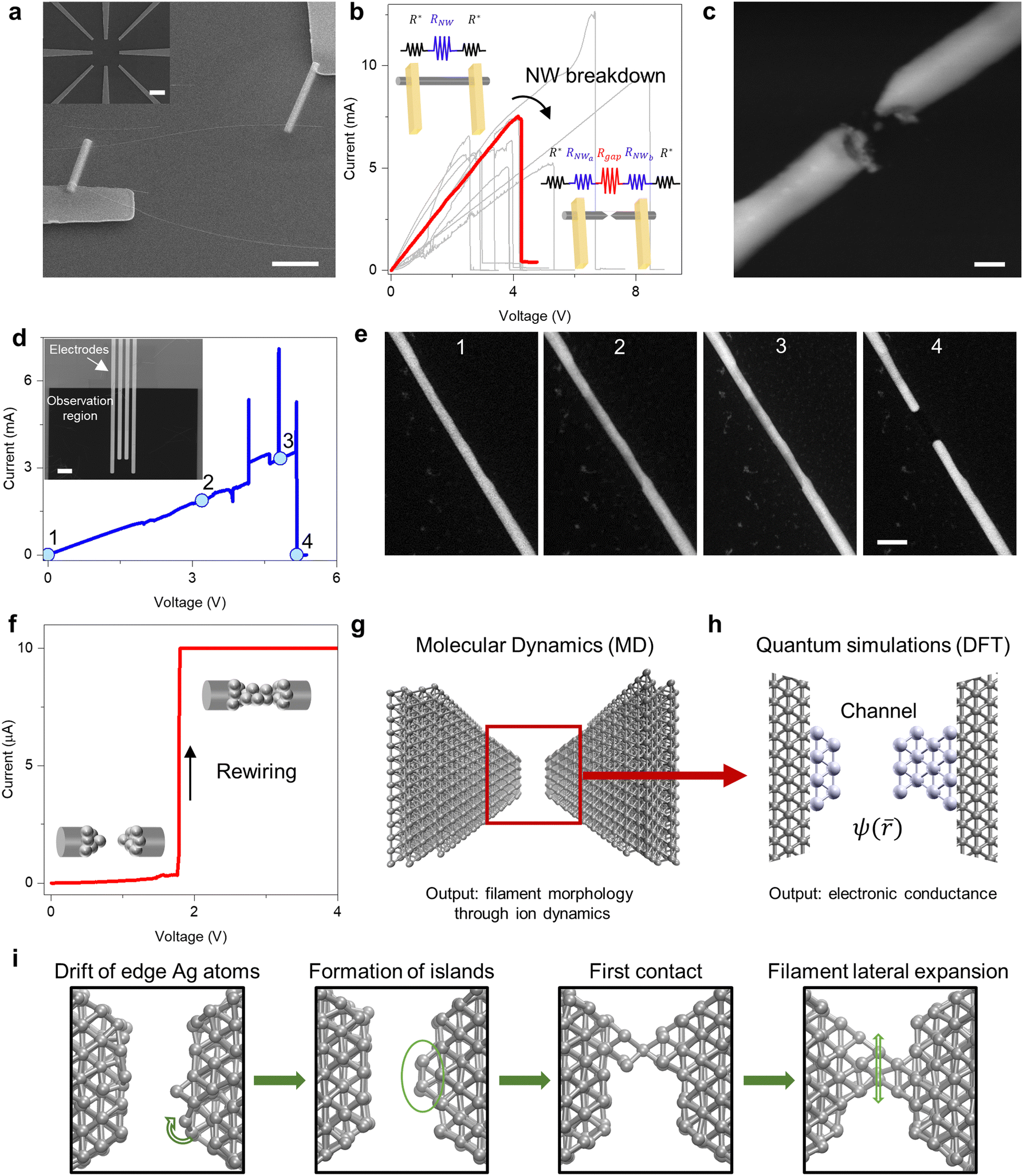 | ||
| Fig. 1 Breakdown and rewiring of single Ag NWs. (a) Scanning Electron Microscopy (SEM) image of a single NW device obtained by connecting an Ag NW to a pre-patterned electrodes by means of IBID deposition of Pt contacts (scale bar, 10 μm). The inset shows a low magnification SEM image of the pre-patterned sub millimetric probe circuit (scale bar, 50 μm). (b) Breakdown of Ag NWs during voltage sweep stimulation, showing a sudden decrease of current due to the formation of an electrically induced nanogap across the NW. The graph shows the NW breakdown of 11 different single Ag NW devices. Insets show the electrical circuital representations of the device before and after breakdown. (c) SEM image of a nanogap across the NW after electrical breakdown (scale bar, 100 nm). (d) Electrical characteristics and corresponding (e) evolution of the Ag NW morphology during breakdown investigated by in situ STEM measurements, showing a thinning effect of the NW until the formation of a nanogap when applying a voltage sweep (scale bar, 200 nm). The inset in panel d shows FESEM image of the chip showing layout of the electrodes on the electron transparent SiN membrane used as observation region (scale bar, 20 μm). (f) Rewiring under voltage sweep stimulation, showing a sudden increase of the device current due to the formation of a conductive filament across the nanogap that re-establish the electrical connection. (g) Conceptual schematization of the simulation approach based on Molecular Dynamics to simulate electrochemical reactions and ionic dynamics across the nanogap. (h) The morphology of conductive filaments across the nanogap is then exploited as input for Density Functional Theory (DFT) that provides quantum transport simulations of ballistic electron transport (i) Dynamics of filament formation under voltage stimulation by MD, showing drift of edge Ag atoms and followed by the formation of islands before the establishment of the first atomic contact. After contact, the filament growth proceeds through lateral expansion. | ||
After breakdown, the electrical connection can be re-established through electrochemical rewiring effects that involves electrochemical dissolution of the positively biased NW needle to form Ag+ ions that migrates across the nanogap under the action of an applied electric field to form a conductive filament that bridges the two NW needles.19 In addition to electrochemical effects, in case of electric field gradients atoms can move to close the nanogap also without direct electrochemical reactions.21 An example of electrochemical rewiring under voltage sweep stimulation is reported in Fig. 1f, where the sudden increase of current occurs when the conductive filament bridges the two NW needles, lowering the gap resistance Rgap and turning the device to a lower resistance state. Note that the here reported mechanism differs from resistive switching usually observed in metal-oxide NWs where switching occurs along the NW surface without initial formation of a nanogap through breakdown events.22–24
In the field of memristive devices, several simulations have been carried out to describe the previously discussed filament growth process.25–27 Also, simulations developed on force-controlled mechanical break junctions have been adapted to electrical-driven atomic memories without considering electrochemical processes.28 However, all these simulative approaches either provide just a description of the ion dynamics or they treat the conduction between electrodes classically. While these simulations showed the formation of QPC as first stage of the filament formation, the strict relationship between morphology of the filament obtained by large scale classical simulations and conductance calculated by more accurate quantum transport simulations has been rarely explored due to the difficulties in connecting the two methodologies.29 Here we report on a combined approach based on classical Molecular Dynamics and quantum transport simulations based on density functional theory have been exploited to unveil the relationship between electrochemical phenomena and ionic dynamics with electronic transport properties across conductive filaments formed within the nanogap. The advantage of such an approach lies in the capability to realistically describe, step by step, the atomic morphology of the system (MD simulation) by considering both electrochemical phenomena and ionic migration, paired with accuracy in the prediction of the electronic properties of the atomic-sized filament (DFT). As schematically reported in Fig. 1g and h the outputs of the MD simulation, i.e., the atomic positions in the filament, serve as input for the DFT computations that provide information on the conductance of the structure. Effects of both the applied voltage and the thermal oscillations are captured by the model. To describe the dynamics of the filament formation process, reactive force field molecular dynamics simulations were employed. In the simulation, the electrode biasing and the electrochemical dissolution of the NW is described by iteratively adjusting the charge on each atom depending on the nearby electrochemical environment and the applied voltage (details in Methods). Such feature distinguishes our model from literature methods that combine MD and ab initio simulations,30,31 allowing for the description of electrochemically induced formation of large-scale filaments. Four stages of the dynamic evolution of the filament under external voltage stimulation can be identified through MD simulation, as illustrated in Fig. 1i. Initially, the device is constituted by two opposing tips separated by a gap, similarly to the experimental nanogap shown in Fig. 1c. As a voltage is applied, Ag adatoms coming from the edge of the metal contact drift toward the tip surface. Once they accumulate on the surface, they start coalescing and forming metastable islands on both sides that shrink the gap between the opposing tips. Eventually, a single atom bridges the two tips reestablishing the electrical connection lost after the breakdown. Finally, because of the applied voltage, other atoms drift toward the filament causing an enlargement of its section. These observations agree with experimental results reported in conventional memristive cells where the conductive filament size can be tailored through appropriate electrical stimulation.32
Notably, while the filament formation occurs by following the same stages, an increase in the applied voltage results in faster kinetics as detailed in Fig. S3 (ESI†). Similarly, a faster formation of the filament is expected by reducing the nanogap length by reducing the tip-to-tip distance due to the increase of the electric field while applying the same voltage bias.
The NW after breakdown acts as an electrochemical memristive cell where the connectivity across the nanogap can be electrochemically weakened or enhanced through rupture/rewiring of the conductive filament connecting the two NW needles under the action of an applied electric field. Rupture/rewiring effects give rise to SET/RESET events that reversibly turns the device from a high resistive state (HRS) to a low resistance state (LRS) and vice versa, where the switching mechanism rely on the electrochemical metallization memory effect.2,22 This results in the typical I–V memristive characteristic under voltage sweep stimulation, as reported in Fig. 2a, where a current compliance (CC) of 400 μA was applied after SET to prevent hard breakdown of the device due to overheating. The switching behavior is maintained over cycling, as revealed by switching the device 100 times between HRS and LRS by means of full-sweep cycles (Fig. 2b). HRS and LRS are stable over time, as revealed by testing for 103 s the retention characteristics (Fig. 2c). Notably, in this case the formed conductive filament after SET events (in the LRS) show conductance values in the range ∼2–3 G0 over rupture/rewiring cycles (Fig. 2d) and over time (Fig. 2e), suggesting that quantum effects regulate electronic transport in the ballistic conduction regime. Experimental results show that fingerprints of quantum conductance effects can be observed by properly tuning stimulation conditions. For example, the G0 conductance level can be achieved by lowering the programming CC (Fig. 2f). Also, quantum conductance levels can be appreciated by slowing down the kinetics of filament formation/rupture during voltage-sweep driven SET and RESET events, as reported in Fig. 2g and h, respectively.
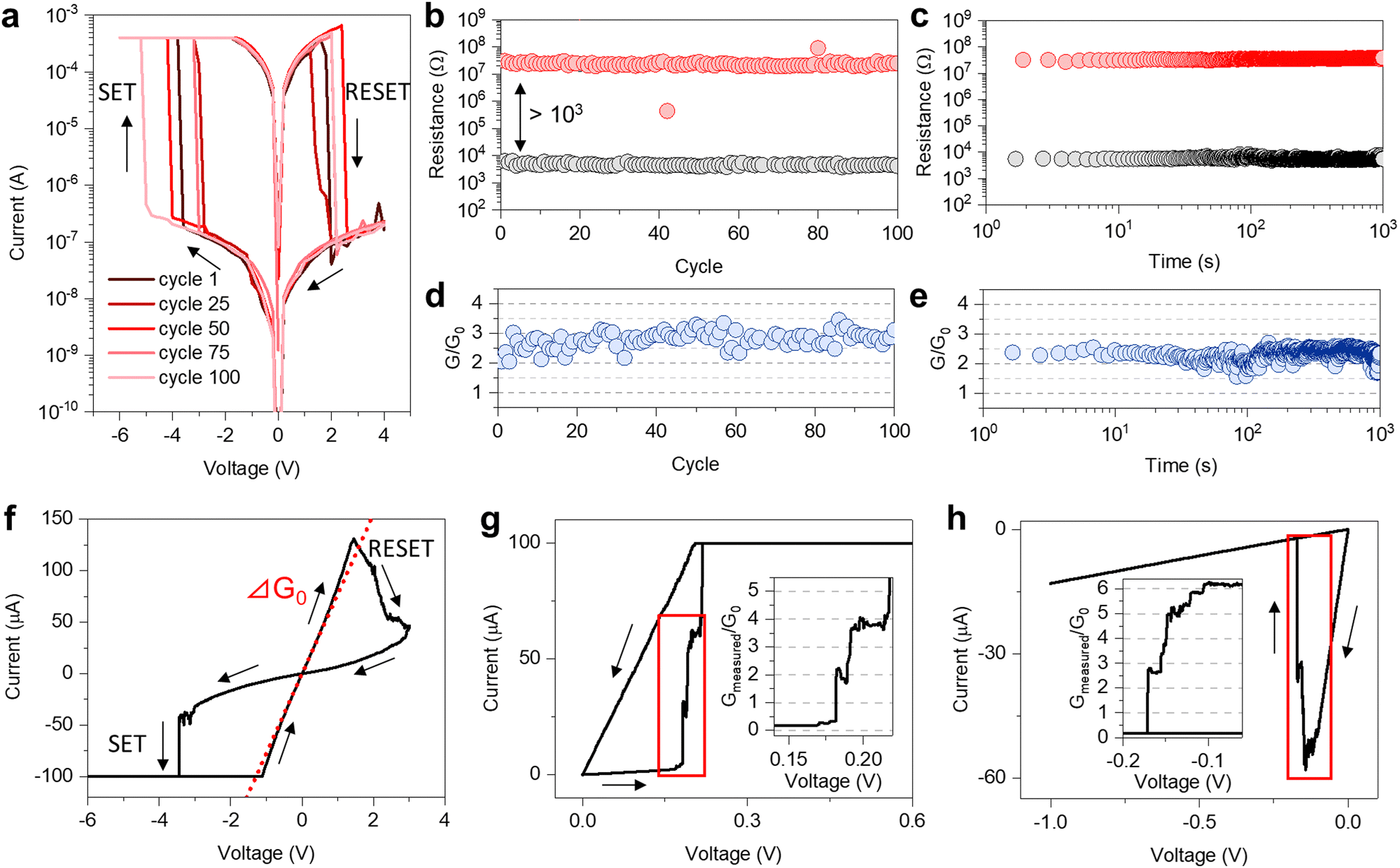 | ||
| Fig. 2 Resistive switching and quantum conductance effects in single memristive Ag NWs. (a) I–V curves obtained by stimulating the Ag NW after breakdown with voltage sweeps, showing resistive switching between a high resistance state (HRS) and a low resistance state (LRS) and vice versa in correspondence of SET and RESET events, respectively. A compliance current (CC) of 400 μA was imposed to prevent hard breakdown of the device during SET events. (b) Endurance properties of the device under 100 full sweep cycle stimulation, where HRS and LRS were evaluated at a reading voltage of 0.4 V (outliers not shown). (c) Retention properties tested by monitoring LRS and HRS states for 103 s by applying a constant voltage of 0.1 V. (d) Normalized conductance state of the conductive filament over rupture/formation cycles, where conductance states corresponds to the LRS of the endurance test reported in panel b. (e) Normalized conductance state of the conductive filament over time, where conductance states corresponds to the LRS of the retention test in panel c. (f) Example of a resistive switching characteristic where the conductance state was programmed to 1 G0 by applying a programming CC of 100 μA. (g) Rewiring of the NW obtained by slowing down the kinetics of filament formation (voltage sweep rate of ∼2.6 mV s−1), allowing the observation of quantum conductance levels during SET. (h) Rupture of the conductive filament across the nanogap by slowing down kinetics, allowing the observation of quantum conductance levels during RESET (voltage sweep rate of ∼4.5 mV s−1). Insets in panels g and h show the details of the step-like evolution of the NW conductance during SET and RESET (red rectangles), respectively. | ||
More discrete conductance levels can be achieved by stimulating the device through current sweeps. In this context, it should be pointed out that the larger number of discrete conductance levels observed under current-controlled stimulation mode, already reported in case of conventional metal–insulator–metal memristive cells based on thin films with Ag electrodes,33 can be related to current-enhanced stability effects involving the interplay between surface tension and quantum pressure forces due to the recoil of flowing charge carriers acting on the quantum point contact.34Fig. 3a reports the NW response after breakdown to a current sweep in the range 0–20 μA. As can be observed, current sweep stimulation induces step-like drops in the measured voltage across the NW. These drops in measured voltage corresponds to the establishment of atomic point contacts resulting in discrete steps of device conductance. In Fig. 3a, a step-like increase of conductance corresponding to four quantum conductance states multiples of G0 can be identified. It is important to point out that the effect of the resistance at the Pt–Ag NW interface (R*) and the resistance of the two NW disconnected parts (RNWa + RNWb) has a progressively higher influence on conductance values of quantum steps corresponding to larger multiples of G0 where the effect of these parasitic resistances becomes progressively comparable with that of the quantum point contact (details in Fig. S4, ESI†). Also, it is important to remark that quantum levels observed through current sweeps does not arise from a purely electronic mechanism, as testified by the hysteretic (memory) behavior of the V–I characteristic (details in Fig. S5, ESI†).
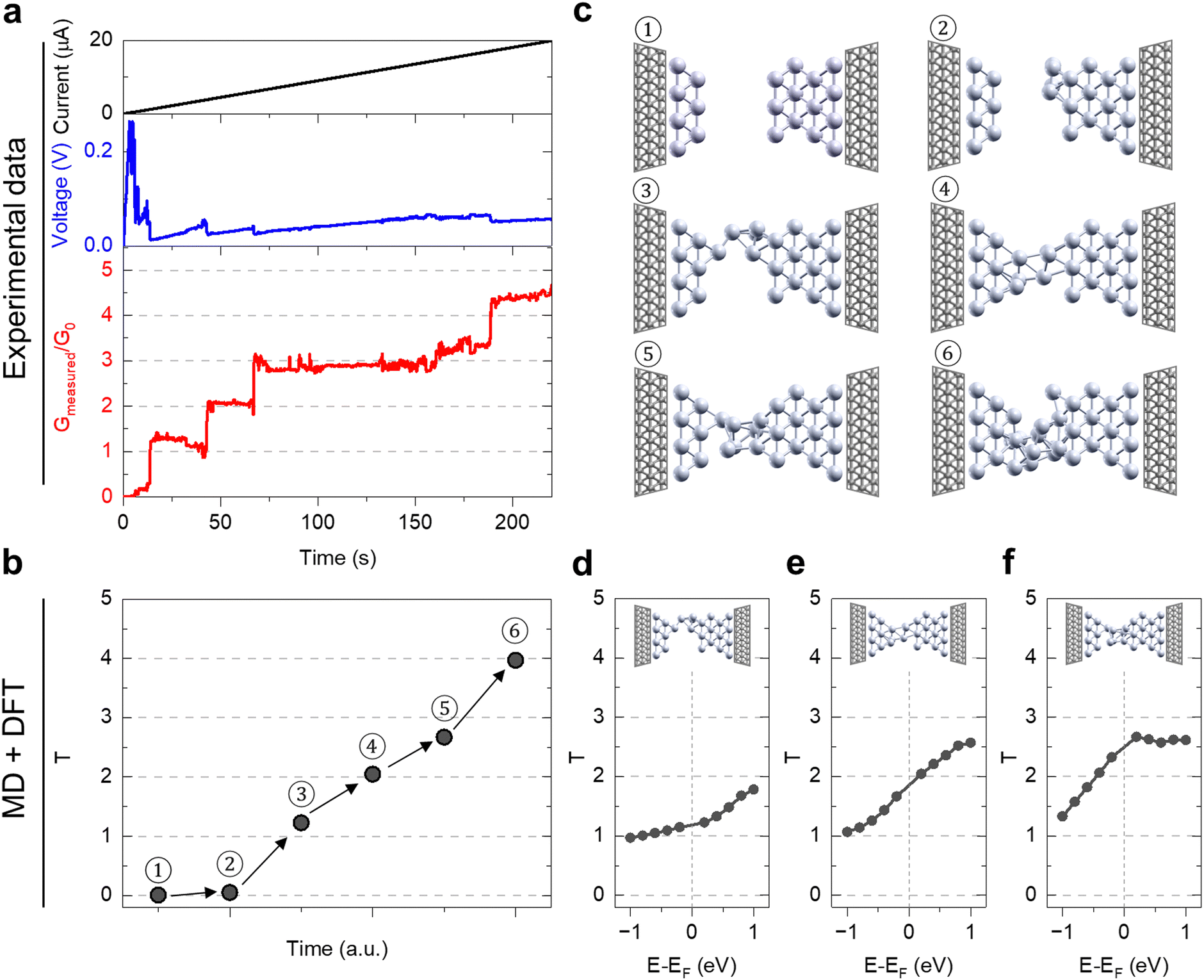 | ||
| Fig. 3 Rewiring through quantum conductance effects. (a) Quantum conductance effects in a current sweep induced NW rewiring. A current sweep in the range 0–20 μA was applied to the NW device (sweep rate of ∼90 nA s−1) while measuring the voltage drop across its electrodes, allowing the monitoring of the device conductance Gmeasured. (b) Evolution of the transmission coefficient during the rewiring process computed by DFT simulations on the structures depicted in (c). Dependence of the transmission coefficient on the applied voltage (d), (e) and (f) respectively for structure 3, 4 and 5 of Panel c. | ||
The experimental data presented above show that rewiring occurs through a step-like increase of conductance where conductance plateaus can be associated to quantum conductance levels. In this context, combined MD and DFT simulations allow a detailed analysis on the dynamic evolution of the filament morphology and reveal how morphology is correlated to ballistic electronic conduction properties. For this purpose, exemplary atomic configurations extracted during the filament evolution obtained by classical MD were used to compute the device transmission coefficient T, where T = G/G0 in the framework of the Landauer-Büttiker theory,35via ballistic DFT simulations. Fig. 3b illustrates the T evolution for the structures reported in Fig. 3c. According to experimental results reported in Fig. 3a, the simulated filament growth proceeds through stages characterized by conductance values close to multiples of G0. Such analogy between experiments and simulations allows to create a link between the measured G and the microscopic structure of the filament. In absence of a chemical connection between tips (structures 1 and 2 of Fig. 3c), T sits around a value of 0. As a chemical bond is formed (structure 3 of Fig. 3c), T jumps close to 1, but it does not assume the exact unitary value, similarly to the experimental device. The subsequent enlargement of the filament under the effect of the applied bias leads to the formation of new chemical bonds, as in structure 4, 5 and 6. The transmission coefficient grows in a stepwise manner accordingly to the number of atoms in the filament. Conduction shows, therefore, a QPC character with discrete levels of T. Note that the increase in T is here connected to a physical modification of the atomic structure of the filament rather than to the progressive population of higher energy bands of the electrode material (as in case of QPC observed in semiconductor devices36). As proof of such statement, T as function of the applied voltage on specific structures are reported in Fig. 3d–f. In the range −1 to 1 eV from the Fermi level, no stepped conductance is found but rather a continuous increase of T as consequence of the higher number of available propagating states for larger bias.
Notably, quantum levels in the experimental device are subjected to cycles-to-cycle variability in terms of both step sequence and current levels where specific steps are observed. For this reason, statistical analysis of quantum steps was performed by considering 116 current-sweep cycles during the SET process (in the range 0–20 μA) acquired on 5 different NW devices, resulting in a total number of more than 464![[thin space (1/6-em)]](https://www.rsc.org/images/entities/char_2009.gif) 000 conductance measurement points. The histogram resulting from a cumulative statistics of measurement points is reported in Fig. 4a, while Fig. 4b reports the distribution of measured point where the effect of parasitic resistances has been subtracted (Note S1, ESI†). As can be observed, these programming conditions result in conductance distributions with a prominent peak close to the resistance of a single atomic point contact G0. Also, peaks at higher multiples of G0 can be identified. Notably, the progressive increase of the influence of parasitic resistances when considering larger conductance values leads to larger differences in the position of conductance peaks corresponding to larger multiples of G0. However, it can be observed that the effect of parasitic resistances has an almost negligible effect on the position of the peak at ∼G0.
000 conductance measurement points. The histogram resulting from a cumulative statistics of measurement points is reported in Fig. 4a, while Fig. 4b reports the distribution of measured point where the effect of parasitic resistances has been subtracted (Note S1, ESI†). As can be observed, these programming conditions result in conductance distributions with a prominent peak close to the resistance of a single atomic point contact G0. Also, peaks at higher multiples of G0 can be identified. Notably, the progressive increase of the influence of parasitic resistances when considering larger conductance values leads to larger differences in the position of conductance peaks corresponding to larger multiples of G0. However, it can be observed that the effect of parasitic resistances has an almost negligible effect on the position of the peak at ∼G0.
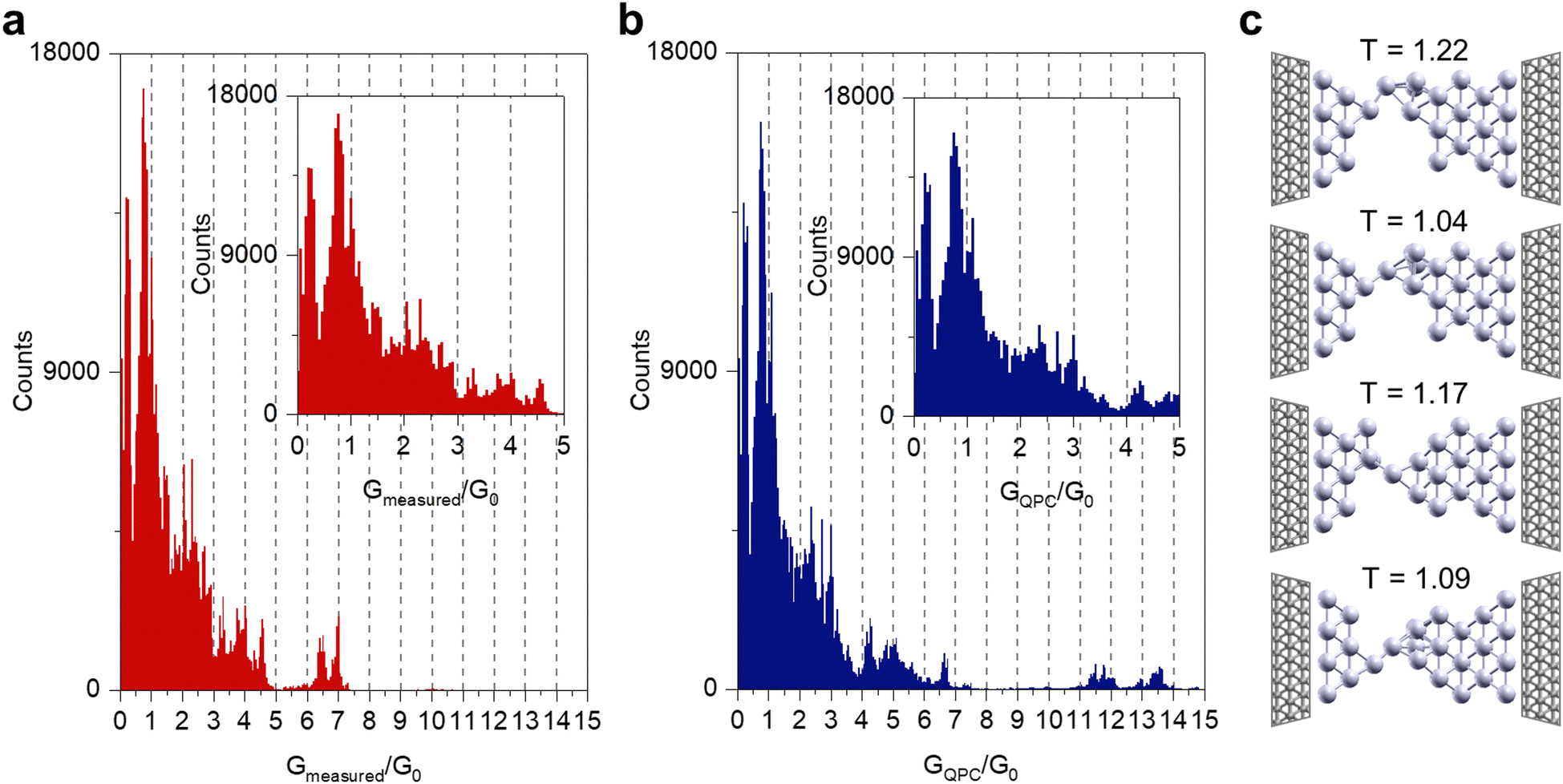 | ||
| Fig. 4 Statistical analysis of quantum levels. Cumulative statistics of (a) measured NW conductance and (b) NW conductance where the effect of parasitic resistances have been subtracted. Histograms with bin size of 0.05 G0 have been created by considering more than 464000 experimental data points acquired on 5 different single NW devices through a current sweep stimulation in the range 0–20 μA as detailed in Fig. 3a. (c) Examples of filament structures derived from the combined MD/DFT simulative approach that shows a transmission coefficient around the value of 1. | ||
The histogram of Fig. 4b is peaked around multiples of G/G0 but it also shows a broad distribution around the peaks due to variations of conductance values across multiple realizations of filaments. Simulations suggest that the broad distribution can arise from fluctuations of the atomic arrangement of the silver filament observed along different MD trajectories during rewiring. These lead to small deviations of T values around multiple integer values of G0. Fig. 4c show examples of atomic configuration of nanofilaments with a single atomic point contact extracted from different MD growth trajectories describing the rewiring process. Notably, even if all the structures are characterized by a single connecting bond, they slightly differ in T Thus, the different local arrangement of the atoms at the QPC resulting from temperature induced restructuring leads to a broad conductance peak due to small variations around G0. Similar considerations can be made for the broad distributions observed around higher G0 multiples. In other words, the broadening around integer values in experimental G/G0 distribution is not related only to measure limitations, but it is caused by the intrinsic variability of the rewiring process.
In addition, fluctuations of conductance values over time in each conductance plateau can be observed. An example of an experimental time trace where the conductance of a specific conductance plateau (∼2.5 G0) was monitored over time with a constant read voltage (0.1 V) is reported in Fig. 5a. As detailed in Fig. 5b, conductance fluctuations over time can be observed. This electronic noise can be ascribed to conductance fluctuations related to dynamics of the Ag nanofilament, as revealed by simulations. The in-silico time trace of T is calculated by fine sampling of the MD trajectory, and it is shown in Fig. 5c. In accordance with experimental results, the simulated time trace shows fluctuations around the ∼2.5 G0 mark. By inspecting the evolution over time of the filament (Fig. 5d, Movie S2, ESI†) it can be observed that changes of T results from variations of the atomic rearrangement in the filament. Such ion dynamics arise from random thermally activated hops of ions under the effect of an electric field which induces disorder.
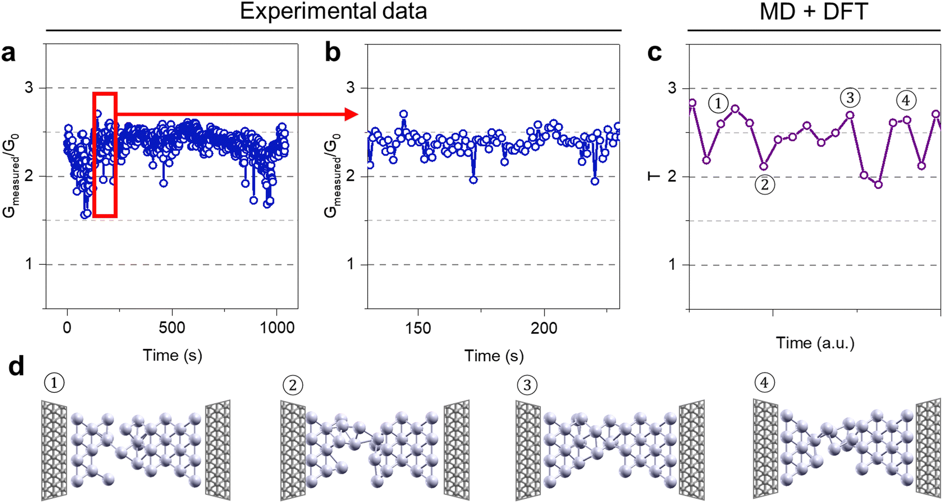 | ||
| Fig. 5 Conductance fluctuations over time. (a) Experimental data showing conductance fluctuations around the ∼2.5 G0 quantum level, where the conductance was monitored with a constant read voltage of 0.1 V (data from Fig. 2e). (b) Zoom of the conductance time trace reported in panel a. (c) Transmission coefficient fluctuations as function of time obtained from MD and DFT simulations. (d) Examples of atomic configurations resulting from the simulations. Numbers refer to the points indicated in Panel c. | ||
Experimental and simulation results show that the process of NW rupture/rewiring proceeds through stages that involves the formation of quantum point contacts, suggesting that quantum effects in nanoobjects play a role in determining the emergent behavior of self-organizing nanonetworks. Differently from conventional memristive cells, single NW memristive devices allow decoupling of the effect of parasitic resistances, showing that the effect of parasitic resistance cannot be neglected in resistive switching devices while evaluating the conductance of quantum plateaus corresponding to high multiples of G0. The combined experimental and theoretical approach shows that (i) the variability of conductance observed during different filament growths and (ii) the conductance fluctuations over time are intrinsic properties of resistive switching cells operating in the quantum regime. Concerning variability, similar behavior was previously reported for simulations of mechanically controlled break junctions where conduction was observed to oscillates around multiples of G0.37 Concerning conductance fluctuations over time, is shown that thermal fluctuations and disorder play a crucial role in determining conductance of resistive switching devices. In this context, the temperature has both the effect of (i) inducing random atomic oscillations and of (ii) increasing the rate of ion drifting in the direction of the electric field.38 Consequently, it contributes to the constant alteration of the morphology of the filament. In this context, our results are in agreement with previous results obtained on Ag filaments in memristive nanojunctions, where current noise spectra revealed that the main electronic noise contribution arises from resistance fluctuations involving atomic rearrangement of nanofilaments.39 It is worth noticing also that quantized conductance was reported to coincides with state instability and excess of noise in memristive devices, as analyzed in redox-based memristive devices involving the migration of oxygen-related species.16 More in general, results show that variability and conductance fluctuations intrinsically related to the switching mechanism at the atomic scale should be considered when evaluating ultimate performances of memristive devices working in the quantum regime. Last, the here proposed computational approach, able to reproduce electrochemical processes and ionic dynamics leading to nanofilament formation while, at the same time, monitoring the electronic transport properties with a quantum approach, open new perspectives for understanding the relationship between nanofilament dynamics and quantum conductance in memristive devices from an atomistic point of view.
In addition, the results reported here can shed new light on conduction properties of self-organizing memristive systems characterized by emergent functionalities arising from the interaction of a huge amount of nanoparts,19,40–45 making these systems suitable physical substrates for neuromorphic-type of data processing and in-materia unconventional computing.43,46–50 Indeed, previous works reported that local switching events can be associated with quantum conductance effects, reflecting in discrete steps and plateaus of the overall effective network conductance, as discussed in case of percolating nanoparticle films,51 nanoparticle networks,52 atomic-switch networks,40 and nanowire networks.53 In case of percolating networks, it has been shown that quantum effects lead to an emergent network behavior characterized by discrete steps in conductance that coincides with integer multiples of G0.51 Also, conductance plateaus at fractions of the quantum conductance levels in the effective network conductance have been proposed to be associated with the formation of macroscopic “winner-takes-all” conductive pathways in NW networks, representing the lowest possible energy connectivity pathways in these nanosystems.53 In this framework, our results shows that quantum conductance effects in single nanowires after breakdown can affect the emerging behavior and neuromorphic functionalities of these self-assembled systems.
Conclusions
In summary, we have reported on quantum effects in single memristive NWs, shedding light on the relationship between quantum phenomena and electrochemical dynamics in memristive devices. Besides experimental investigation of quantum phenomena, a simulation approach for memristive devices that combines MD to investigate ionic dynamics underlaying switching with DFT simulations to unveil the structure-dependent conductance of nanofilaments has been reported. The combined experimental and modeling approach revealed that deviations from integer multiples of the fundamental quantum of conductance depend on the peculiar dynamic trajectory of nanofilaments and that conductance fluctuations in quantum plateaus rely on thermal fluctuations involving atomic reconfiguration at the quantum point contact. Besides providing a complete description of ionic/electronic conduction mechanisms in NWs for rational design of neuromorphic architectures, these results establish a strict relationship between quantum phenomena and ionic dynamics in memristive devices.Methods
Experimental setup and electrical characterization
Memristive devices based on single Ag NWs were fabricated by combining lithography techniques and ion beam induced deposition. Initially, sub-millimeter probe circuits were fabricated on commercial Si/SiO2 (1 μm) substrates through laser writing lithography (Heidelberg upg101) and ti/Au deposition by RF sputtering. Then, Ag NWs in isopropyl alcohol suspension (Sigma-Aldrich) were deposited on pre-patterned substrates by drop-casting and spontaneous solvent evaporation. Selected NWs were then connected to pre-patterned electrodes by means of Ion Beam-Induced Deposition (IBID) of Pt through a gas injection system (GIS), on a FEI Quanta 3D system. During IBID, Ga+ ions react with the metal–organic precursor in the chamber, (CH3)3Pt(CPCH3), leading to the conductive metal deposition that ensure good electrical contact with Ag wire at the same time avoiding any interaction of the nanostructure with resist and solvents. Electrical measurements have been performed by means of a Keithley 4200-SCS Parameter Analyzer and a probe-station. All electrical measurements were performed in air at room temperature.In situ TEM measurements
TEM measurements were performed using a Tecnai F20 microscope (FEI), operated at 200 kV acceleration voltage. High-angle annular dark field (HAADF) detector was used in Scanning TEM (STEM) mode. Dedicated sample holder (FUSION – PROTOCHIPS) was used for applying bias to the NWs. In this case, NWs were dispersed on commercial e-chips consisting of a Si3N4 membrane on which 4 Pt electrodes with a 5 mm spacing are present (e-chip E-FED01-LN Protochips). Then electron induced Pt deposition was applied to bound the NWs with the existing electrodes. This was performed by means of IBID using Zeiss Auriga dual-beam system at 1.5 kV. In situ electrical measurements were performed in two-probe configuration by means of a Keithley 2614b source-measurement unit, by stimulating the device with a voltage sweep with rate of ∼17 mV s−1. In situ breakdown experiments were carried out in vacuum conditions.Molecular dynamics and density functional theory simulations
The evolution of the filament morphology is described by classical molecular dynamics simulations using the LAMMPS package.54 The filament is described as two pyramidal silver tips having a 4.2 nm × 4.2 nm base as shown in Fig. 1e. A gap of 8.3 Å separates the two tips. The positions of the atoms at the base of the pyramids are fixed to keep the two tips in place for the entire simulation. Interatomic interactions are described with the REAXFF potential55 parametrized in ref. 56 that allows for the formation and rupture of bonds in Ag. The potential employs the charge equilibration method to alter, at each step, the charge of the atoms depending on the local environment.57 N. Onofrio et al.58 further developed the algorithm to include the possibility of applying a potential difference between two metal leads and to simulate the electrochemical dissolution of ions of the metal. Thanks to this algorithm, for instance, metal ions in the bulk of the contact, at the surface or dissolved in an electrolyte show distinct amounts of charges. In order for the dissolution process to take place within the timescale of the MD simulations, a voltage of 2 V (or 8 V) and a thermostat with temperature of 800 K are applied. The use of high temperatures is a common technique employed in computational research that is aimed at accelerating the dynamics of rare events such as ion drift and diffusion through hopping, chemical reactions or mixing.59 Temperature is maintained constant with a Nosé–Hoover thermostat. The structure is equilibrated for 50 ps and, afterward, a production run of 3 ns is carried out. A timestep of 1 fs is used to sample the trajectory. Every 8.6 ps, the positions of the atoms that moved within the gap separating the metal tips, are extracted and used as input for the quantum transport simulations. Because of the temperature accelerated dynamics, the meaning of timescale is lost. As such we chose to indicate time in arbitrary units in Fig. 5c. DFT simulations were performed with the QUANTUM ESPRESSO package.60 Specifically, the ballistic conductance was calculated with the PWCOND code included in QUANTUM ESPRESSO.61 The filament is described as two symmetrical leads and a channel. The leads are made by a three-layered bulk of silver in a 3 × 3 supercell with the (111) plane in contact with the channel. The base structure of the channel is composed by a few layers of Ag (see Fig. 1f) separated by the same gap used in MD simulation. In each quantum calculation, the gap is filled with additional silver atoms whose positions are taken from the MD simulations to provide a time trace of the transmission coefficient on the basis on the evolution of the filament described by classical molecular dynamics, i.e., DFT calculations have been performed on snapshots of conductive filament morphologies obtained by MD. The DFT computations are performed within the PBE formulation62 of the general gradient approximation that was proved to reliably describe the electronics of memristive materials in NWs.63,64 A plane-waves basis set with a 28 Ry cutoff was used to describe the electronic wave functions and with a 280 Ry cutoff to represent the density. Electron–ion interaction has been described by ultrasoft pseudopotentials.65 For the calculation of the ballistic conductance, 135 independent k-points were used.Data availability
The data that support the findings of this study are available on Zenodo (https://doi.org/10.5281/zenodo.10489181).Author contributions
G. M. and F. R. generated the idea and designed the experiments. G. M. performed experimental analysis while F. R performed simulations. G. M. and F. R. provided interpretation of results and wrote the manuscript. K. B. performed in situ TEM experiments. I. D. C. and M. F. supported experimental fabrication of devices. G. M. provided funding. All authors participated in the discussion of results and revision of the manuscript.Conflicts of interest
There are no conflicts of interest to declare.Acknowledgements
Part of this work was supported by the European project MEMQuD, code 20FUN06. This project (EMPIR 20FUN06 MEMQuD) has received funding from the EMPIR programme co-financed by the Participating States and from the European Union's Horizon 2020 research and innovation programme. Part of this work was supported by the Italian Ministry of University and Research, PRIN 20229JRTZA “NEURONE”. Part of this work has been carried out at Nanofacility Piemonte INRiM, a laboratory supported by the ‘‘Compagnia di San Paolo’’ Foundation, and at the QR Laboratories, INRiM.References
- Z. Wang, H. Wu, G. W. Burr, C. S. Hwang, K. L. Wang, Q. Xia and J. J. Yang, Nat. Rev. Mater., 2020, 5, 173–195 CrossRef CAS.
- I. Valov, R. Waser, J. R. Jameson and M. N. Kozicki, Nanotechnology, 2011, 22, 289502 CrossRef.
- M.-K. Song, J.-H. Kang, X. Zhang, W. Ji, A. Ascoli, I. Messaris, A. S. Demirkol, B. Dong, S. Aggarwal, W. Wan, S.-M. Hong, S. G. Cardwell, I. Boybat, J. Seo, J.-S. Lee, M. Lanza, H. Yeon, M. Onen, J. Li, B. Yildiz, J. A. del Alamo, S. Kim, S. Choi, G. Milano, C. Ricciardi, L. Alff, Y. Chai, Z. Wang, H. Bhaskaran, M. C. Hersam, D. Strukov, H.-S. P. Wong, I. Valov, B. Gao, H. Wu, R. Tetzlaff, A. Sebastian, W. Lu, L. Chua, J. J. Yang and J. Kim, ACS Nano, 2023, 17(13), 11994–12039 CrossRef CAS PubMed.
- M. Lanza, A. Sebastian, W. D. Lu, M. Le Gallo, M.-F. Chang, D. Akinwande, F. M. Puglisi, H. N. Alshareef, M. Liu and J. B. Roldan, Science, 2022, 376(6597), eabj9979 CrossRef CAS PubMed.
- G. Milano, M. Aono, L. Boarino, U. Celano, T. Hasegawa, M. Kozicki, S. Majumdar, M. Menghini, E. Miranda, C. Ricciardi, S. Tappertzhofen, K. Terabe and I. Valov, Adv. Mater., 2022, 34, 2201248 CrossRef CAS PubMed.
- T. N. Török, M. Csontos, P. Makk and A. Halbritter, Nano Lett., 2020, 20, 1192–1200 CrossRef PubMed.
- J. J. T. Wagenaar, M. Morales-Masis and J. M. Van Ruitenbeek, J. Appl. Phys., 2012, 111(1), 014302 CrossRef.
- W. Xue, S. Gao, J. Shang, X. Yi, G. Liu and R. Li, Adv. Electron. Mater., 2019, 5, 1800854 CrossRef.
- Y. Li, S. Long, Y. Liu, C. Hu, J. Teng, Q. Liu, H. Lv, J. Suñé and M. Liu, Nanoscale Res. Lett., 2015, 10, 420 CrossRef PubMed.
- A. Mehonic, A. Vrajitoarea, S. Cueff, S. Hudziak, H. Howe, C. Labbé, R. Rizk, M. Pepper and A. J. Kenyon, Sci. Rep., 2013, 3, 2708 CrossRef CAS PubMed.
- A. Geresdi, A. Halbritter, A. Gyenis, P. Makk and G. Mihály, Nanoscale, 2011, 3, 1504–1507 RSC.
- C. Hu, M. D. McDaniel, A. Posadas, A. A. Demkov, J. G. Ekerdt and E. T. Yu, Nano Lett., 2014, 14, 4360–4367 CrossRef CAS PubMed.
- K. Krishnan, M. Muruganathan, T. Tsuruoka, H. Mizuta and M. Aono, Adv. Funct. Mater., 2017, 27, 1605104 Search PubMed.
- W. Banerjee and H. Hwang, Adv. Electron. Mater., 2019, 5, 1900744 CrossRef CAS.
- J. B. Roldán, D. Maldonado, A. Cantudo, Y. Shen, W. Zheng and M. Lanza, Appl. Phys. Lett., 2023, 122(20), 203502 CrossRef.
- W. Yi, S. E. Savel’ev, G. Medeiros-Ribeiro, F. Miao, M.-X. Zhang, J. J. Yang, A. M. Bratkovsky and R. S. Williams, Nat. Commun., 2016, 7, 11142 CrossRef CAS PubMed.
- J. Zhao, H. Sun, S. Dai, Y. Wang and J. Zhu, Nano Lett., 2011, 11, 4647–4651 Search PubMed.
- N. M. Batra, A. Syed and P. M. F. J. Costa, Nanoscale, 2019, 11, 3606–3618 RSC.
- G. Milano, G. Pedretti, M. Fretto, L. Boarino, F. Benfenati, D. Ielmini, I. Valov and C. Ricciardi, Adv. Intell. Syst., 2020, 2, 2000096 CrossRef.
- D. Xiang, X. Wang, C. Jia, T. Lee and X. Guo, Chem. Rev., 2016, 116, 4318–4440 CrossRef CAS PubMed.
- Y. Yang, P. Gao, L. Li, X. Pan, S. Tappertzhofen, S. Choi, R. Waser, I. Valov and W. D. Lu, Nat. Commun., 2014, 5, 4232 Search PubMed.
- G. Milano, M. Luebben, Z. Ma, R. Dunin-Borkowski, L. Boarino, C. F. Pirri, R. Waser, C. Ricciardi and I. Valov, Nat. Commun., 2018, 9, 5151 Search PubMed.
- G. Milano, F. Raffone, M. Luebben, L. Boarino, G. Cicero, I. Valov and C. Ricciardi, ACS Appl. Mater. Interfaces, 2020, 12, 48773–48780 CrossRef CAS PubMed.
- G. Milano, L. Boarino and C. Ricciardi, Nanotechnology, 2019, 30, 244001 CrossRef CAS PubMed.
- N. Onofrio, D. Guzman and A. Strachan, Nat. Mater., 2015, 14, 440–446 CrossRef CAS PubMed.
- Y.-L. Chen, B. Balraj, P.-F. Chung, C. Sivakumar, W.-J. Lee and M.-S. Ho, Appl. Phys. Lett., 2021, 118, 083502 CrossRef CAS.
- F. Raffone and G. Cicero, ACS Appl. Mater. Interfaces, 2018, 10, 7512–7519 CrossRef CAS PubMed.
- C. Schirm, M. Matt, F. Pauly, J. C. Cuevas, P. Nielaba and E. Scheer, Nat. Nanotechnol., 2013, 8, 645–648 CrossRef CAS PubMed.
- M. Kaniselvan, M. Luisier and M. Mladenović, Solid-State Electron., 2023, 199, 108506 CrossRef CAS.
- M. Kaniselvan, M. Luisier and M. Mladenović, Solid-State Electron., 2023, 199, 108506 CrossRef CAS.
- O. G. Kharlanov, JETP Lett., 2023, 117, 384–391 CrossRef CAS.
- D. Ielmini, Semicond. Sci. Technol., 2016, 31, 063002 CrossRef.
- S. Tappertzhofen, I. Valov and R. Waser, Nanotechnology, 2012, 23, 145703 CrossRef CAS PubMed.
- O. G. Kharlanov, B. S. Shvetsov, V. V. Rylkov and A. A. Minnekhanov, Phys. Rev. Appl., 2022, 17, 054035 CrossRef.
- R. Landauer, IBM J. Res. Dev., 1957, 1, 223–231 Search PubMed.
- H. van Houten and C. Beenakker, Phys. Today, 1996, 49, 22–27 CrossRef CAS.
- F. Pauly, M. Dreher, J. K. Viljas, M. Häfner, J. C. Cuevas and P. Nielaba, Phys. Rev. B: Condens. Matter Mater. Phys., 2006, 74, 235106 CrossRef.
- F. Raffone and G. Cicero, ACS Appl. Mater. Interfaces, 2018, 10, 7512–7519 Search PubMed.
- B. Sánta, Z. Balogh, A. Gubicza, L. Pósa, D. Krisztián, G. Mihály, M. Csontos and A. Halbritter, Nanoscale, 2019, 11, 4719–4725 RSC.
- A. Z. Stieg, A. V. Avizienis, H. O. Sillin, C. Martin-Olmos, M. Aono and J. K. Gimzewski, Adv. Mater., 2012, 24, 286–293 CrossRef CAS PubMed.
- S. K. Bose, C. P. Lawrence, Z. Liu, K. S. Makarenko, R. M. J. van Damme, H. J. Broersma and W. G. van der Wiel, Nat. Nanotechnol., 2015, 10, 1048–1052 Search PubMed.
- J. Hochstetter, R. Zhu, A. Loeffler, A. Diaz-Alvarez, T. Nakayama and Z. Kuncic, Nat. Commun., 2021, 12, 4008 CrossRef CAS PubMed.
- A. Loeffler, A. Diaz-Alvarez, R. Zhu, N. Ganesh, J. M. Shine, T. Nakayama and Z. Kuncic, Sci. Adv., 2023, 9(16), eadg3289 CrossRef PubMed.
- G. Milano, A. Cultrera, L. Boarino, L. Callegaro and C. Ricciardi, Nat. Commun., 2023, 14, 5723 Search PubMed.
- G. Milano, E. Miranda and C. Ricciardi, Neural Networks, 2022, 150, 137–148 CrossRef PubMed.
- G. Milano, G. Pedretti, K. Montano, S. Ricci, S. Hashemkhani, L. Boarino, D. Ielmini and C. Ricciardi, Nat. Mater., 2022, 21, 195–202 Search PubMed.
- G. Milano, K. Montano and C. Ricciardi, J. Phys. D: Appl. Phys., 2023, 56, 084005 CrossRef.
- S. Lilak, W. Woods, K. Scharnhorst, C. Dunham, C. Teuscher, A. Z. Stieg and J. K. Gimzewski, Frontiers in Nanotechnology, 2021, 3, 1–11 CrossRef.
- G. Milano, M. Agliuzza, N. de Leo and C. Ricciardi, in 2022 International Joint Conference on Neural Networks (IJCNN), IEEE, 2022, pp. 1–6.
- G. Milano, S. Porro, I. Valov and C. Ricciardi, Adv. Electron. Mater., 2019, 5, 1800909 CrossRef.
- A. Sattar, S. Fostner and S. A. Brown, Phys. Rev. Lett., 2013, 111, 136808 CrossRef PubMed.
- J. B. Mallinson, S. Shirai, S. K. Acharya, S. K. Bose, E. Galli and S. A. Brown, Sci. Adv., 2019, 5, eaaw8438 CrossRef CAS PubMed.
- H. G. Manning, F. Niosi, C. G. da Rocha, A. T. Bellew, C. O’Callaghan, S. Biswas, P. F. Flowers, B. J. Wiley, J. D. Holmes, M. S. Ferreira and J. J. Boland, Nat. Commun., 2018, 9, 3219 CrossRef PubMed.
- A. P. Thompson, H. M. Aktulga, R. Berger, D. S. Bolintineanu, W. M. Brown, P. S. Crozier, P. J. in’t Veld, A. Kohlmeyer, S. G. Moore, T. D. Nguyen, R. Shan, M. J. Stevens, J. Tranchida, C. Trott and S. J. Plimpton, Comput. Phys. Commun., 2022, 271, 108171 CrossRef CAS.
- T. P. Senftle, S. Hong, M. M. Islam, S. B. Kylasa, Y. Zheng, Y. K. Shin, C. Junkermeier, R. Engel-Herbert, M. J. Janik, H. M. Aktulga, T. Verstraelen, A. Grama and A. C. T. Van Duin, npj Comput. Mater., 2016, 2 Search PubMed.
- A. Lloyd, D. Cornil, A. C. T. Van Duin, D. Van Duin, R. Smith, S. D. Kenny, J. Cornil and D. Beljonne, Surf. Sci., 2016, 645, 67–73 CrossRef CAS.
- A. K. Rappe and W. A. Goddard, J. Phys. Chem., 1991, 95, 3358–3363 CrossRef CAS.
- N. Onofrio and A. Strachan, J. Chem. Phys., 2015, 143, 054109 Search PubMed.
- F. Raffone, A. Lamberti and G. Cicero, Electrochim. Acta, 2023, 458, 142344 Search PubMed.
- P. Giannozzi, S. Baroni, N. Bonini, M. Calandra, R. Car, C. Cavazzoni, D. Ceresoli, G. L. Chiarotti, M. Cococcioni, I. Dabo, A. Dal Corso, S. de Gironcoli, S. Fabris, G. Fratesi, R. Gebauer, U. Gerstmann, C. Gougoussis, A. Kokalj, M. Lazzeri, L. Martin-Samos, N. Marzari, F. Mauri, R. Mazzarello, S. Paolini, A. Pasquarello, L. Paulatto, C. Sbraccia, S. Scandolo, G. Sclauzero, A. P. Seitsonen, A. Smogunov, P. Umari and R. M. Wentzcovitch, J. Phys.: Condens. Matter, 2009, 21, 395502 Search PubMed.
- A. Smogunov, A. Dal Corso and E. Tosatti, Phys. Rev. B: Condens. Matter Mater. Phys., 2004, 70, 045417 CrossRef.
- J. P. Perdew, K. Burke and M. Ernzerhof, Phys. Rev. Lett., 1996, 77, 3865–3868 Search PubMed.
- F. Raffone, F. Risplendi and G. Cicero, Nano Lett., 2016, 16, 2543–2547 CrossRef CAS PubMed.
- F. Raffone and G. Cicero, Solid State Ionics, 2017, 299, 93–95 CrossRef CAS.
- D. Vanderbilt, Phys. Rev. B: Condens. Matter Mater. Phys., 1990, 41, 7892–7895 CrossRef PubMed.
Footnote |
| † Electronic supplementary information (ESI) available: Pristine state of single Ag NW memristive devices (Fig. S1), in situ STEM measurements (Fig. S2), effect of the applied voltage on filament formation (Fig. S3). Effect of parasitic resistances on quantum conductance levels (Fig. S4), hysteretic memory effect (Fig. S5), pristine state resistance values (Table S1), Subtraction of parasitic resistance effects on the nanogap resistance (Note S1). Movie S1. In situ STEM video showing the breakdown process. The in situ STEM movie illustrating the breakdown process induced by ramping the bias from 0 V till the breakdown with a ramp rate of ∼17 mV s−1. It shows changes in the morphology of the Ag NW during the voltage stimulation ramp, with the final breakdown at 5.17V. The movie playback rate is in real time. Movie S2. Evolution of the nanofilament over time leading to conductance fluctuations. Movie of MD simulation of the electrochemical rewiring process in the timeframe illustrated in Fig. 5c. The movie shows the effect of the temperature fluctuations on the morphology that, ultimately, affect the overall conductance of the system. See DOI: https://doi.org/10.1039/d3nh00476g |
| This journal is © The Royal Society of Chemistry 2024 |