
 Open Access Article
 This Open Access Article is licensed under a
 Creative Commons Attribution 3.0 Unported Licence
Tailoring giant quantum transport anisotropy in nanoporous graphenes under electrostatic disorder†
Isaac
Alcón
 *a,
Aron W.
Cummings
*a and
Stephan
Roche
ab
*a,
Aron W.
Cummings
*a and
Stephan
Roche
ab
aCatalan Institute of Nanoscience and Nanotechnology (ICN2), CSIC and BIST, Campus UAB, Bellaterra, 08193 Barcelona, Spain. E-mail: isaac.alcon@icn2.cat; aron.cummings@icn2.cat
bICREA, Institució Catalana de Recerca i Estudis Avançats, 08070 Barcelona, Spain
First published on 23rd January 2024
Abstract
During the last 15 years bottom-up on-surface synthesis has been demonstrated as an efficient way to synthesize carbon nanostructures with atomic precision, opening the door to unprecedented electronic control at the nanoscale. Nanoporous graphenes (NPGs) fabricated as two-dimensional arrays of graphene nanoribbons (GNRs) represent one of the key recent breakthroughs in the field. NPGs interestingly display in-plane transport anisotropy of charge carriers, and such anisotropy was shown to be tunable by modulating quantum interference. Herein, using large-scale quantum transport simulations, we show that electrical anisotropy in NPGs is not only resilient to disorder but can further be massively enhanced by its presence. This outcome paves the way to systematic engineering of quantum transport in NPGs as a novel concept for efficient quantum devices and architectures.
New conceptsThe ability to tailor quantum transport in carbon 2D nanostructures is a key step towards the future realization of carbon nanoelectronics and spintronics. While enormous progress has been made in realizing multiple types of carbon nanomaterials with different electronic properties, little is known about how such versatility at the nanoscale could be translated into tunable transport characteristics. Here, via efficient quantum transport simulations, we demonstrate that chemically modified nanoporous graphenes (NPGs) allow for an effective control over in-plane quantum transport: that is, control over the preferred direction for charges to propagate. Concretely, we find, for the first time, that the inherent quantum transport anisotropy in NPGs not only survives but becomes enhanced under electrostatic disorder conditions, which is essential for its technological applicability in real devices. Additionally, for specific chemically tuned NPGs, we show that anisotropy becomes giant, meaning that transport can strictly only take place along one in-plane direction. Our results thus provide a general recipe to engineer quantum transport in carbon 2D nanostructures with atomic precision, thus opening a new avenue in the field of 2D materials. |
Introduction
Bottom-up on-surface synthesis is a powerful tool to fabricate carbon nanostructures with atomic precision.1–3 During the last 15 years, this method has allowed the synthesis of different types of nanomaterials such as 2D covalent organic frameworks,4–6 magnetic nanographenes,7,8 1D π-conjugated polymers,9,10 and graphene nanoribbons (GNRs),2,11 among others.12,13 GNRs, concretely, have gathered great attention for carbon nanoelectronics,14,15 given their semiconducting electronic structure and chemical stability which has facilitated their integration in various solid-state devices.16–18 The electronic structure of GNRs has also been shown to be highly tunable by bottom-up design, permitting the realization of topologically non-trivial states,19,20 which has created high expectations for their use in quantum technologies.21,22Another related family of carbon nanomaterial which could strongly benefit from the key features of GNRs is the family of nanoporous graphenes (NPGs). NPGs, first reported in 2018,23 are formed as 2D arrays of GNRs laterally connected via π-conjugated covalent bonds, thus creating a regular array of pores in the otherwise graphene-like 2D structure. Since the pioneering work, different types of NPGs have been reported,24,25 and have been integrated in solid-state devices exploiting their semiconducting characteristics.23,26 An important property of the NPGs is their in-plane charge transport anisotropy. It was theoretically shown that current preferentially flows along the GNRs, but due to their electronic coupling it also spreads in the transversal direction.27 Importantly, due to the fully π-conjugated nature of NPGs, such inter-ribbon coupling may be tuned by bridging the GNRs with π-conjugated molecular bridges, as done in the past with GNR pairs.28 For example, single phenyl rings determine the strength of inter-ribbon transport depending on their connectivity,29 due to destructive quantum interference (QI).30para connections lead to a constructive interference of the two propagating paths through the phenyl ring, thus enhancing electronic transmission.31 Contrarily, the electronic waves have opposite phases upon propagating through meta-connected phenyl rings, destructively interfering (QI) and leading to an effective depletion of transmission.31 Consequently, the para configuration leads to transversal spreading in the so-called para-NPG material (as in the original NPG27), whereas the meta configuration cuts inter-ribbon coupling due to QI, leading to almost complete 1D transport in the resulting meta-NPG.29 Importantly, NPGs including para- and meta-connections between GNRs have recently been synthesized,32 highlighting the experimental feasibility of such QI-engineering of NPGs.
Despite the great promise of these strategies to realize highly tunable platforms based on NPGs for multiple applications, it remains unclear whether QI-engineering is robust under realistic material and device conditions. Indeed, to date all theoretical transport studies have exclusively considered the pristine (ultra-clean) systems,27,29,33 without evaluating how static or dynamic disorder could influence NPGs' electrical characteristics. In particular, electrostatic disorder, which may arise from interactions with underlying substrates or via chemical/atomic adsorbates,34 could strongly influence the effectiveness of QI-engineering.29,32 More generally, a priori it is difficult to predict the effect of local impurity scattering on the transport along each in-plane direction in NPGs. Therefore, evaluating the impact of disorder on electrical transport in NPGs is of primary importance to discern their future applicability in various emerging fields such as nanoelectronics, nanosensing, spintronics and quantum technologies.
Here we evaluate, via efficient large-scale quantum transport simulations, the effect of electrostatic disorder on the transport characteristics of three different types of NPGs: the original fabricated NPG, the para-NPG, and the meta-NPG. We focus our study on the mono-phenylated NPGs,29 which allows us to isolate the role of QI from other physico-chemical phenomena reported for bi-phenylated NPGs such as the out-of-plane rotation of molecular bridges.32 Our quantum simulations are based on an efficient wave packet propagation method and the use of the Kubo formalism that gives access to the length- and energy-dependent-conductivity of disordered systems containing many millions atoms.35 Electrostatic disorder is modelled as local electron–hole puddles randomly distributed throughout each sample. By simulating the time evolution of wave packets, we obtain fundamental insight into the transport dynamics, and we characterize the transport regime for each material and in-plane direction. Altogether, we find that the electrical anisotropy in NPGs is strongly enhanced by the presence of electrostatic disorder. This derives from the stronger effect of charged impurities on transport between GNRs than along GNRs. While this is true for all considered NPGs and should be general for this class of 2D materials, the transport anisotropy is maximum for the meta-NPG case. In this material transport through the bridges is much more sensitive to disorder than in the other NPGs, making it fully insulating in one in-plane direction, while remaining a semiconductor in the other direction (along the GNRs). Consequently, to the best of our knowledge, meta-NPG is the first 2D material displaying an unprecedented giant quantum transport anisotropy, reaching the limit of behaving as a 2D array of purely isolated 1D nanoelectronic channels conveying charges in parallel. Overall, our results indicate that the use of NPGs to design circuit architectures based on guided transport and controlled switching through 1D channels is feasible under realistic experimental conditions.
Results and discussion
Fig. 1a depicts the atomic structure of our considered materials which, with graphene as a reference, include the original NPG23 and the subsequently predicted and chemically tailored para-NPG and meta-NPG.29 Structurally, NPGs may be thought of as a 2D grid of parallel GNRs laterally connected via strong covalent bonding. While in NPG the GNRs are directly linked via single C–C bonds, in para- and meta-NPGs the GNRs are bridged via a phenylene ring in para- and meta-configuration, respectively (Fig. 1a-top). As previously shown,27,29 the basic electronic structure of NPGs is properly captured with a standard first nearest-neighbour tight-binding (TB) Hamiltonian, as normally used for graphene: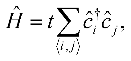 | (1) |
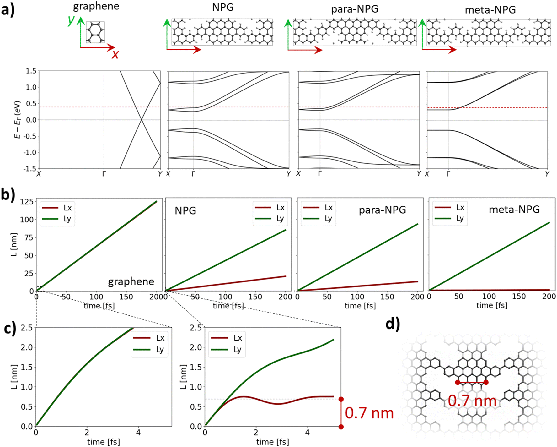 | ||
| Fig. 1 (a) Periodic structure of each material (top) and associated band structure (bottom) obtained from the 1st nearest-neighbour TB model (tij = −2.7 eV, ε0 = 0 eV). As highlighted with coloured arrows, the y (x) axis is parallel (perpendicular) to the GNRs in NPGs. The red dashed line indicates the energy at which the wave packet propagation is calculated (E − EF = 0.4 eV). (b) Wave packet displacement along each in-plane direction (Lx: red curves; Ly: green curves). (c) Wave packet propagation lengths for the first 5 fs of the run in graphene and the NPG. The black dotted line indicates the average width of the GNR composing all NPGs, as depicted in (d). | ||
To evaluate the effect of disorder on the quantum transport properties of NPGs, we make use of a real-space order-N wave packet propagation methodology, generally known as the linear-scaling quantum transport (LSQT) method, pioneered decades ago for the study of aperiodic and disordered materials.36–38 LSQT is based on the Kubo formalism and allows the simulation of quantum transport in complex disordered systems composed of many millions of atoms. Its various implementations have been recently presented in.ref. 35 The central quantity of this method is the energy- and time-dependent mean squared displacement, which is here computed in the two in-plane directions,
 | (2) |
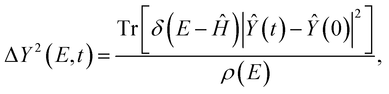 | (3) |
![[X with combining circumflex]](https://www.rsc.org/images/entities/i_char_0058_0302.gif) (t) are the position operators along (y) and perpendicular to (x) the GNRs direction, respectively, and ρ(E) = Tr[δ(E − Ĥ)] is the density of states of the system at a given energy. We then obtain the propagation length along each direction as
(t) are the position operators along (y) and perpendicular to (x) the GNRs direction, respectively, and ρ(E) = Tr[δ(E − Ĥ)] is the density of states of the system at a given energy. We then obtain the propagation length along each direction as | (4) |
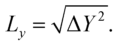 | (5) |
| Graphene | NPG | para-NPG | meta-NPG | |
|---|---|---|---|---|
| n x /ny | 174/200 | 92/345 | 75/345 | 75/345 |
| A/B [nm] | 300.6/299.3 | 301.6/299.9 | 301.9/299.9 | 301.9/299.9 |
| N at | 3![[thin space (1/6-em)]](https://www.rsc.org/images/entities/char_2009.gif) 340800 340800 |
2539200 |
2380500 |
2380500 |
Due to the electron–hole symmetry present in all considered systems (see band structures in Fig. 1a) we limit our discussion to energies lying in the conduction bands, with the resulting conclusions also applicable to the valence bands. We consider quantum transport at E − EF = 0.4 eV (see dashed red line in Fig. 1a), while in the ESI† we show qualitatively similar results for E − EF = 0.7 eV.
Fig. 1b shows the evolution of Ly(t) (green) and Lx(t) (red) for each pristine material. While for graphene the evolution of Ly(t) and Lx(t) exactly overlap, for the NPGs Lx(t) is always significantly smaller than Ly(t). Zooming in on the first 5 fs (Fig. 1c) we find that this divergence takes place around the first femtosecond when the wave packet reaches 0.7 nm, corresponding to the average width of the GNRs, as highlighted in Fig. 1d. This ultra-fast process of hitting the GNR wall is common to all NPGs (see Fig. S1 in ESI†). However, while the Ly(t) evolution is similar for all NPGs, Lx(t) monotonically decreases from NPG to meta-NPG (Fig. 1b), where Lx(t) appears as a nearly flat curve. This reflects the fact that while para-connected phenylene rings slightly decrease inter-ribbon transmission as compared to direct C–C bonding (para-NPG vs. NPG), the meta-configuration almost entirely suppresses inter-ribbon transport. This difference between NPGs, not noticeable for very short times (Fig. S1, ESI†), becomes clear around 10–20 fs (Fig. S2, ESI†). As previously mentioned, such differences emerge from the destructive interference between electronic waves crossing meta-connected bridges (QI),30 as long studied in the field of single-molecule electronics.39
To quantify the electrical anisotropy of the pristine systems, we first extract the Fermi velocity along each direction as
 | (6) |
![[v with combining macron]](https://www.rsc.org/images/entities/i_char_0076_0304.gif) y and x. Table 2 shows the resulting anisotropy values for each material.
y and x. Table 2 shows the resulting anisotropy values for each material.
| Graphene | NPG | para-NPG | meta-NPG | |
|---|---|---|---|---|
|
A = y/x |
1.0 | 4.1 | 7.1 | 120.0 |
These values agree with the qualitative picture previously obtained from Ly(t) and Lx(t) (Fig. 1b) and are fundamentally the same for states deeper within the conduction band (see Table S1 for E − EF = 0.7 eV, ESI†). These anisotropy values are also in line with previous predictions for other phenylated NPGs which were recently experimentally fabricated,32 and are of the same order of magnitude as other low-symmetry 2D materials proposed for in-plane anisotropic electronics,40 including black phosphorous.41 However, it is worth highlighting the special case of meta-NPG (see Table 2 and Table S1, ESI†) where the anisotropy is at least one order of magnitude larger than the other NPGs and most low-symmetry 2D materials.40
It is known that electrostatic disorder may severely affect transport anisotropy in 2D materials, up to the point of reversing the preferential direction for current flow.41 Such disorder may arise in experiments from interaction with the underlying substrate,34 or due to molecular/atomic adsorbates.42 Therefore, it is imperative to evaluate whether the high anisotropy of NPGs survives under these conditions. Electrostatic disorder may be effectively modelled via a random distribution of Gaussian-like electron–hole puddles. These are included in the TB model by modifying the on-site terms as
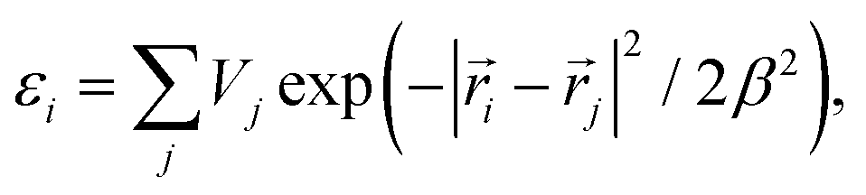 | (7) |
![[r with combining right harpoon above (vector)]](https://www.rsc.org/images/entities/i_char_0072_20d1.gif) i is the position of each carbon site, j is the position of each puddle centre, β is the puddle width set to 4.35 Å, and Vj is the potential height, which is randomly distributed between −2.8 and +2.8 eV (see Methods for further details). We use a puddle density of 0.1% which, as shown in previous studies,43 leads to charge mobility values in graphene similar to experiments.42 For illustration, a puddle distribution obtained with these parameters is shown in Fig. 2a for one-fourth of the total area of our NPG sample (see square outline at bottom left in Fig. 2a). There we see that the puddles have an average diameter similar to the GNR width.
i is the position of each carbon site, j is the position of each puddle centre, β is the puddle width set to 4.35 Å, and Vj is the potential height, which is randomly distributed between −2.8 and +2.8 eV (see Methods for further details). We use a puddle density of 0.1% which, as shown in previous studies,43 leads to charge mobility values in graphene similar to experiments.42 For illustration, a puddle distribution obtained with these parameters is shown in Fig. 2a for one-fourth of the total area of our NPG sample (see square outline at bottom left in Fig. 2a). There we see that the puddles have an average diameter similar to the GNR width.
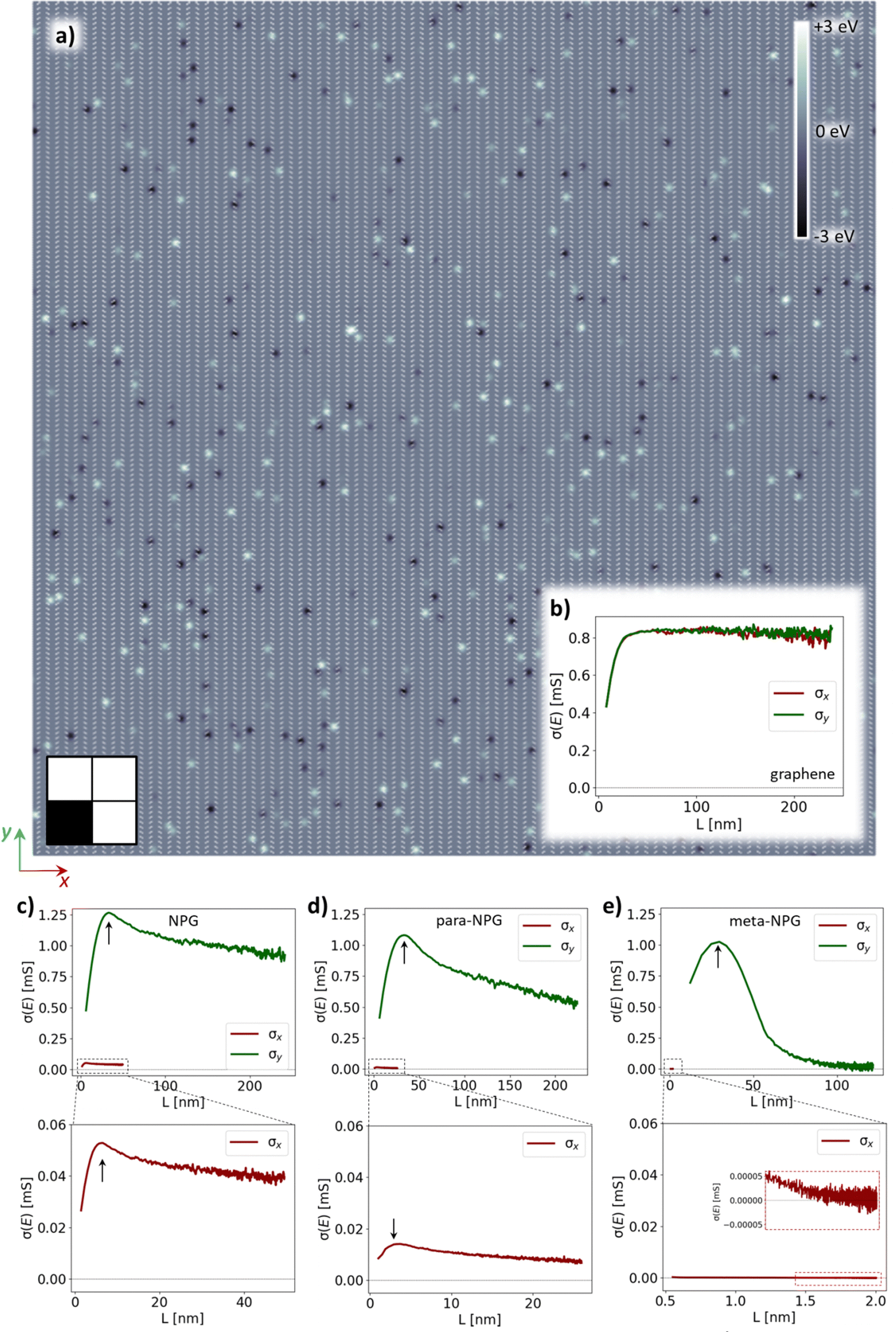 | ||
| Fig. 2 (a) Puddle distribution map for one-fourth of the total area (300 × 300 nm2) of the NPG sample (see square outline at bottom left). Bright and dark regions are associated with p-doping (εi > 0) and n-doping (εi < 0), respectively. Evolution of σy (green curves) and σx (red curves) with wave packet length at E − EF = 0.4 eV for (b) graphene, (c) NPG, (d) para-NPG and (e) meta-NPG. For the last three cases, an additional σx(Lx) plot is provided at the bottom for better visualization and comparison. | ||
Under such disorder, transport in 2D materials evolves from the ballistic regime, characteristic of pristine systems, to the diffusive or even localization regimes depending on the system length and disorder strength.35 The transport regime can be actually extracted from the scaling of the diffusion coefficient, which is obtained from the time evolution of the mean squared displacement as
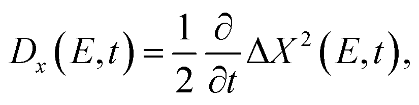 | (8) |
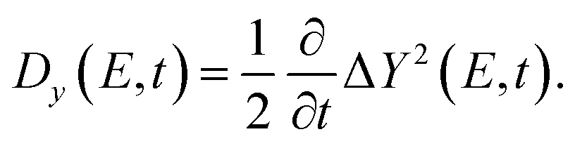 | (9) |
| σx(E,t) = e2ρ(E)Dx(E,t), | (10) |
| σy(E,t) = e2ρ(E)Dy(E,t), | (11) |
Fig. 2 shows σx(Lx) and σy(Ly) for each material under the influence of electrostatic disorder. We consider 10 random puddle distributions to obtain statistically averaged quantities (see Methods for details). In Fig. 2b, graphene undergoes a fast transition from a ballistic transport regime to a diffusive one, where conductivity remains approximately constant with increasing L. Additionally, there is no significant difference between σx and σy, indicating the isotropic nature of this material. This picture changes dramatically for NPGs (Fig. 2c–e) where there is a substantial difference in transport along each in-plane direction, with σx ≪ σy. If we focus on transport along GNRs (σy; green curves), we see that the evolution of conductivity is also very different as compared to graphene. All NPGs (Fig. 2c–e) present a maximum in σy, known as the semi-classical conductivity (σscy; see arrows), followed by a continuous decay of σy with increasing Ly. As explained in detail in Section S2 of the ESI,† this trend may be ascribed to the strong localization regime of transport. In this regime, quantum interference caused by random scattering events35 eventually leads to full confinement of charge carriers (i.e. σ ≈ 0). Experimentally, this corresponds to an exponential increase in resistance with device size. Looking at σx (red curves), one can note the strong reduction of transport in this in-plane direction as compared to σy for all NPGs (Fig. 2c–e). As shown in the bottom panel of Fig. 2c (NPG), σx follows a similar trend as σy but with a much lower magnitude. This decrease in σx is even more pronounced for para-NPG (bottom panel in Fig. 2d), highlighting the less conductive character of para-connected phenyl rings as compared to direct C–C bonding. Finally, in the meta-NPG (Fig. 2e) σx becomes completely suppressed, reaching the situation where σx ≈ 0 (see inset in bottom panel of Fig. 2e). This result demonstrates the efficacy of QI to effectively cut transport between GNRs, even under the presence of strong electrostatic disorder. As with σy, the decay rate of σx for all three NPGs may be associated with the strong localization regime (see Section S2 in the ESI† and further discussion below). It is also worth noting that upon reducing transport between GNRs (i.e. σmetaNPGx < σparaNPGx < σNPGx), transport along the GNRs also becomes increasingly degraded with disorder (i.e. σmetaNPGy < σparaNPGy < σNPGy). In other words, the more 1D-like the electronic system is, the more sensitive it becomes to disorder, which may be explained by the higher probability of back-scattering.44 This also explains the difference in σy between all NPGs and graphene where, due to its purely 2D transport nature, localization effects are much weaker (Fig. 2b).
Defining the charge transport anisotropy in such a complex scenario is not straightforward. One way is to consider the ratio between semi-classical values of conductivity along each in-plane direction,
 | (12) |
Table 3 provides the resulting anisotropy values. While graphene's characteristic isotropic transport remains unchanged, both NPG and para-NPG become more anisotropic than in their pristine form (see Table 2 for comparison). This indicates that disorder perturbs transport more effectively between GNRs than along GNRs. This may be quantified via the ratio of momentum relaxation times which may be extracted from the relation σscy/σscx = (νy/νx)2·τy/τx. We obtain τy/τx values of 1.4 and 1.5 for the NPG and para-NPG, respectively.
| Graphene | NPG | para-NPG | meta-NPGa | |
|---|---|---|---|---|
| a Note: ∞ reflects the fact that meta-NPG does not display a diffusive peak for σx(Lx) and so qualitatively σscx ≈ 0. If one calculates anisotropy A as σscy/σmaxx, then A = 3781.3. However, this value is not representative of the actual anisotropy in this system, as σmaxx here is associated with the initial ultra-fast ballistic regime that quickly evolves to full confinement where σx(Lx) = 0 (see inset in bottom panel of Fig. 2e). | ||||
|
1.0 | 23.7 | 76.7 | ∞ |
Meanwhile, the meta-NPG exhibits unique behavior. In this material there is effectively no diffusive maximum because transport directly transits from “ballistic spreading” at short times to a fully confined situation, as may be seen in the inset of Fig. 2e (bottom panel). Therefore, one may argue that σscx ≈ 0 and, due to the finite σscy (see arrow in Fig. 2e, green curve) one could conclude that A ≈ ∞ for this 2D material. This peculiar result indicates that meta-NPG behaves as a semiconductor along the GNRs, but as an electrical insulator in the perpendicular direction. This highlights that the small (but finite) transmission across GNRs in meta-NPG in the pristine form is fully disrupted by electrostatic disorder, thus leading to an exponential decay of transport across GNRs in this material. Such mechanism effectively leads to the null conductivity along that direction (and so A ≈ ∞).
Although stating that A ≈ ∞ for meta-NPG may appear excessive, there is an alternative way to look at the problem at hand that supports this conclusion. Fig. 3 shows the comparison between the wave packet propagation lengths perpendicular to the GNR (Lx in Fig. 3a) and parallel to them (Ly in Fig. 3b) for different puddle distributions (light curves) and the resulting average (darker curves). As expected from σx(Lx) (red curve in Fig. 2e), we see that Lx saturates to a length of approximately 2 nm. This distance exactly coincides with the distance between two phenylene rings bound to a single GNR (see the unit cell at the top of Fig. 3c). It is also worth noting that all puddle distributions converge to approximately the same value of 2 nm. At E − EF = 0.7 eV Lx saturates to 3 nm (Fig. S7, ESI†) meaning that deeper in the conduction band charge carriers manage to reach the first neighbouring GNR, but do not propagate beyond that limit.
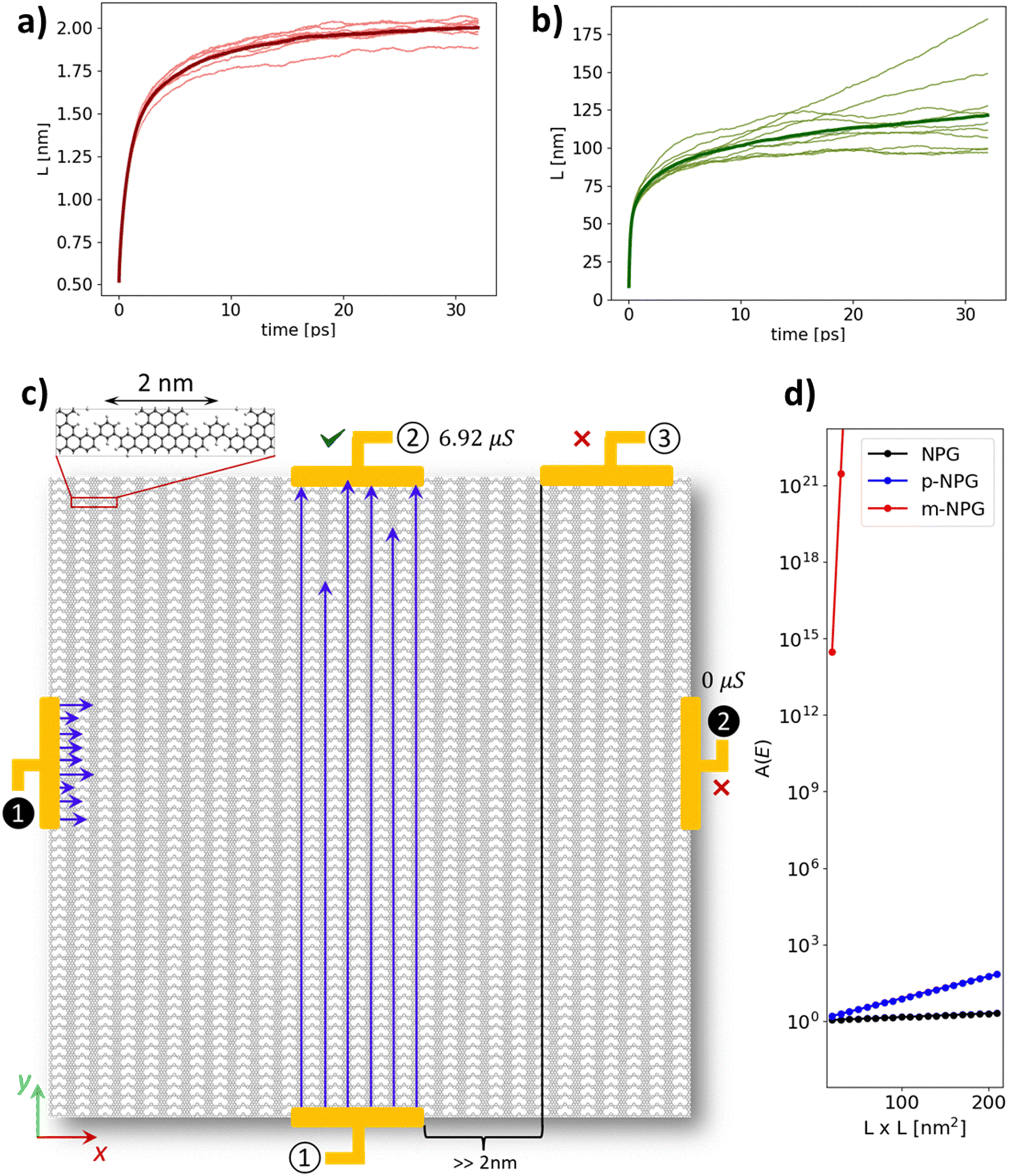 | ||
Fig. 3 Time evolution of wave packet propagation lengths for meta-NPG at E − EF = 0.4 eV for different puddle distributions (light curves) and their average (dark curves) along (a) the direction perpendicular to the GNRs (Lx) and (b) parallel to them (Ly). (c) Schematic of a 50 × 50 nm2meta-NPG device displaying the expected electrical output for different electrode setups measuring transport along the GNRs (① → ②) and perpendicular to them ( → →  ) including extrapolated conductance values (see Section S2 in ESI†). (d) Transport anisotropy (log-scale) at E − EF = 0.4 eV with square device length (i.e. L × L nm2) for NPG (black), the para-NPG (blue) and the meta-NPG (red). Anisotropy is calculated as the ratio between the extrapolated conductance values along each in-plane direction (A = Gy/Gx). See eqn (13) and Section S2 (ESI†) for details. ) including extrapolated conductance values (see Section S2 in ESI†). (d) Transport anisotropy (log-scale) at E − EF = 0.4 eV with square device length (i.e. L × L nm2) for NPG (black), the para-NPG (blue) and the meta-NPG (red). Anisotropy is calculated as the ratio between the extrapolated conductance values along each in-plane direction (A = Gy/Gx). See eqn (13) and Section S2 (ESI†) for details. | ||
On the contrary, Ly grows beyond 100 nm (Fig. 3b) and, additionally, different puddle distributions lead to dispersive saturation lengths ranging from 80 nm to a few hundred nanometers. Such variability between different puddle distributions for transport along GNRs (Fig. 3b) is not present for the other NPGs (Fig. S8, ESI†), which highlights that this is a unique feature of meta-NPG arising from its quasi-1D electrical nature (see Section S3 for further Details and discussion, ESI†).
This significant difference in saturation length between the two in-plane directions should entirely determine the behaviour of meta-NPG-based devices. If one were to measure transport in a 50 × 50 nm2meta-NPG device, as depicted in Fig. 3c, a finite electrical signal should be detected between electrodes ① and ②, since the average puddle propagation along the GNRs, Ly, grows beyond 100 nm (Fig. 3b). In the strong localization regime this may be estimated by fitting the exponentially decaying length-dependent conductance (Gx(Ly) and Gx(Lx)),
| G(E,L) ∝ exp[−L/ξ(E)], | (13) |
 and
and  (Fig. 3c), unveiling the giant transport anisotropy existing in this meta-NPG device (A = G50nmy/G50nmx = ∞). Intuitively, this should not be restricted only for our chosen device configuration, but for any situation where the distance between
  and
and  is larger than 5–10 nm since, as shown in Fig. 3a, Lx is fully saturated at 2 nm (3 nm at E − EF = 0.7 eV; see Fig. S7, ESI†). This fundamentally disruptive result (A ≈ ∞) is unique to meta-NPG, because the other NPGs have finite conductance values along both in-plane directions at similar lengths (see Table S3 in ESI†), leading to relatively moderate/low anisotropy values for device sizes where meta-NPG already displays giant anisotropy (see Fig. 3d). It is also worth noting that finite temperatures should more effectively wash out long-range localization effects than short-range effects.44 Therefore, thermal dephasing should improve transport along the GNRs (i.e. higher Gy(L) values) rather than improving transport perpendicular to them (Gx(L)) which, if anything, would even further increase anisotropy. Again, this scenario only applies to meta-NPG, where the main interference effect suppressing charge transport between GNRs occurs within single (meta-connected) phenyl rings composed of six carbon atoms. Finally we note that transport along y would only be measurable when the same set of GNRs (or first neighbouring ribbons) are contacted (e.g. ① to ② in Fig. 3c). Therefore, no current should be measurable between ① and ③ since the transverse distance between these two electrodes is significantly higher than the Lx saturation value of 2 nm (see Fig. 3c).
Finally, we note that this picture, as determined by the saturation values of Lx and Ly, also holds for weaker disorder conditions (Section S4 in ESI,† Fig. S9 and S11). However, for very strong disorder the wave-packet spreading along the GNRs may decrease to a scale comparable to the GNR width and, in that scenario, giant transport anisotropy in meta-NPG vanishes (Section S4 in ESI,† Fig. S10).
Conclusions
We have evaluated unprecedented charge transport anisotropy of NPGs in the presence of electrostatic disorder expected in realistic devices based on these materials. Our results demonstrate that anisotropy survives disorder and is even strongly enhanced for all NPGs, which implies the technological applicability of this appealing feature (such as for guided transport or directional switching). However, we also find that the conductivity of these materials is significantly degraded due to the presence of electrostatic disorder. Our simulations demonstrate that the considered materials can be classified according to increasing 1D electronic character: graphene → NPG → para-NPG → meta-NPG. Such 1D nature is the main cause for the overall degradation of transport, as compared to graphene, in full accordance with transport theory of 1D systems.44 We also find that chemically-driven bridge engineering – which leads to quantum interference (QI) engineering – is a powerful tool to tailor anisotropy in these materials under experimentally realistic conditions. While para-NPG behaves as a semiconductor along both in-plane directions, meta-NPG displays conducting character only along the GNRs, and is an insulator in the perpendicular direction. This is demonstrated by the full confinement of wave packets in that direction, whose propagation is entirely saturated after 2 to 3 nm, which is approximately the distance between a pair of GNRs. These results thus highlight meta-NPG as an exemplary 2D material featuring giant transport anisotropy (A ≈ ∞).All in all, this work highlights the potential of para- and meta-connected phenyl rings as tools to chemically engineer the transport properties of carbon nanostructures. Indeed, these concepts should be applicable to other carbon nanomaterials such as 2D covalent organic frameworks, nanographenes, 1D π-conjugated polymers, and GNR heterojunctions. More generally, our results also demonstrate the power of inheriting well-established ideas from single-molecule electronics as a guideline to design carbon nanostructures with desired functionality. We believe such a multidisciplinary approach will play a central role in the future realization of carbon-based nanoelectronics and quantum technologies.
Conflicts of interest
There are no conflicts of interest to declare.Acknowledgements
I. A. is grateful for a Juan de la Cierva postdoctoral grant (FJC2019-038971-I) from the Ministerio de Ciencia e Innovación and acknowledges access to supercomputer resources as provided through a grant (TEMP-2023-1-0028) from the Red Española de Supercomputación (RES). ICN2 is funded by the CERCA Programme from Generalitat de Catalunya, has been supported by the Severo Ochoa Centres of Excellence programme [SEV-2017-0706] and is currently supported by the Severo Ochoa Centres of Excellence programme, Grant CEX2021-001214-S, both funded by MCIN/AEI/10.13039.501100011033. We also acknowledge Project PID2019-106684GB-I00 funded by MICIN/ AEI /10.13039/501100011033 and MICIN for NextGenerationEU (PRTR-C17.I1) as well as Generalitat de Catalunya.References
- L. Grill, et al., Nano-architectures by covalent assembly of molecular building blocks, Nat. Nanotechnol., 2007, 2, 687–691 CrossRef CAS PubMed.
- J. Cai, et al., Atomically precise bottom-up fabrication of graphene nanoribbons, Nature, 2010, 466, 470–473 CrossRef CAS PubMed.
- X. H. Liu, C. Z. Guan, D. Wang and L. J. Wan, Graphene-like single-layered covalent organic frameworks: synthesis strategies and application prospects, Adv. Mater., 2014, 26, 6912–6920 CrossRef CAS PubMed.
- Q. Fan, J. M. Gottfried and J. Zhu, Surface-Catalyzed C–C Covalent Coupling Strategies toward the Synthesis of Low-Dimensional Carbon-Based Nanostructures, Acc. Chem. Res., 2015, 48, 2484–2494 CrossRef CAS PubMed.
- G. Galeotti, et al., Synthesis of mesoscale ordered two-dimensional π-conjugated polymers with semiconducting properties, Nat. Mater., 2020, 19, 874–880 CrossRef CAS PubMed.
- K. Niu, et al., Unveiling the formation mechanism of the biphenylene network, Nanoscale Horiz., 2023, 8, 368–376 RSC.
- S. Mishra, et al., Topological frustration induces unconventional magnetism in a nanographene, Nat. Nanotechnol., 2020, 15, 22–28 CrossRef CAS PubMed.
- J. Li, et al., Uncovering the Triplet Ground State of Triangular Graphene Nanoflakes Engineered with Atomic Precision on a Metal Surface, Phys. Rev. Lett., 2020, 124, 177201 CrossRef CAS PubMed.
- C. Steiner, et al., Hierarchical on-surface synthesis and electronic structure of carbonyl-functionalized one- and two-dimensional covalent nanoarchitectures, Nat. Commun., 2017, 8, 14765 CrossRef CAS PubMed.
- B. Cirera, et al., Tailoring topological order and π-conjugation to engineer quasi-metallic polymers, Nat. Nanotechnol., 2020, 15, 437–443 CrossRef CAS PubMed.
- A. Narita, X.-Y. Wang, X. Feng and K. Müllen, New advances in nanographene chemistry, Chem. Soc. Rev., 2015, 44, 6616–6643 RSC.
- Q. Fan, et al., Biphenylene network: a nonbenzenoid carbon allotrope, Science, 2021, 372, 852–856 CrossRef CAS PubMed.
- P. Kuang, et al., Graphdiyne: a superior carbon additive to boost the activity of water oxidation catalysts, Nanoscale Horiz., 2018, 3, 317–326 RSC.
- A. Celis, et al., Graphene nanoribbons: fabrication, properties and devices, J. Phys. D: Appl. Phys., 2016, 49, 143001 CrossRef.
- Z. Chen, A. Narita and K. Müllen, Graphene Nanoribbons: On-Surface Synthesis and Integration into Electronic Devices, Adv. Mater., 2020, 32, 2001893 CrossRef CAS PubMed.
- J. P. Llinas, et al., Short-channel field-effect transistors with 9-atom and 13-atom wide graphene nanoribbons, Nat. Commun., 2017, 8, 633 CrossRef PubMed.
- J. Zhang, et al., Tunable Quantum Dots from Atomically Precise Graphene Nanoribbons Using a Multi-Gate Architecture, Adv. Electron. Mater., 2023, 2201204, DOI:10.1002/aelm.202201204.
- V. Saraswat, R. M. Jacobberger and M. S. Arnold, Materials Science Challenges to Graphene Nanoribbon Electronics, ACS Nano, 2021, 15, 3674–3708 CrossRef CAS PubMed.
- D. J. Rizzo, et al., Topological band engineering of graphene nanoribbons, Nature, 2018, 560, 204–208 CrossRef CAS PubMed.
- O. Gröning, et al., Engineering of robust topological quantum phases in graphene nanoribbons, Nature, 2018, 560, 209–213 CrossRef PubMed.
- J. Li, et al., Topological phase transition in chiral graphene nanoribbons: from edge bands to end states, Nat. Commun., 2021, 12, 1–8 CrossRef PubMed.
- H. Wang, et al., Graphene nanoribbons for quantum electronics, Nat. Rev. Phys., 2021, 3, 791–802 CrossRef CAS.
- C. Moreno, et al., Bottom-up synthesis of multifunctional nanoporous graphene, Science, 2018, 360, 199–203 CrossRef CAS PubMed.
- P. H. Jacobse, et al., Bottom-up Assembly of Nanoporous Graphene with Emergent Electronic States, J. Am. Chem. Soc., 2020, 142, 13507–13514 CrossRef CAS PubMed.
- M. Tenorio, et al., Atomically Sharp Lateral Superlattice Heterojunctions Built-In Nitrogen-Doped Nanoporous Graphene, Adv. Mater., 2022, 34, 2110099 CrossRef CAS PubMed.
- Z. Mutlu, et al., Bottom-Up Synthesized Nanoporous Graphene Transistors, Adv. Funct. Mater., 2021, 2103798, DOI:10.1002/adfm.202103798.
- G. Calogero, et al., Electron Transport in Nanoporous Graphene: Probing the Talbot Effect, Nano Lett., 2018, 19, 576–581 CrossRef PubMed.
- M. Shekhirev, P. Zahl and A. Sinitskii, Phenyl Functionalization of Atomically Precise Graphene Nanoribbons for Engineering Inter-ribbon Interactions and Graphene Nanopores, ACS Nano, 2018, 12, 8662–8669 CrossRef CAS PubMed.
- G. Calogero, I. Alcón, N. Papior, A.-P. Jauho and M. Brandbyge, Quantum Interference Engineering of Nanoporous Graphene for Carbon Nanocircuitry, J. Am. Chem. Soc., 2019, 141, 13081–13088 CrossRef CAS PubMed.
- Y. Tsuji, R. Hoffmann, M. Strange and G. C. Solomon, Close relation between quantum interference in molecular conductance and diradical existence, Proc. Natl. Acad. Sci. U. S. A., 2016, 11, E413–E419 Search PubMed.
- G. C. Solomon, C. Herrmann, T. Hansen, V. Mujica and M. A. Ratner, Exploring local currents in molecular junctions, Nat. Chem., 2010, 2, 223–228 CrossRef CAS PubMed.
- C. Moreno, et al., Molecular Bridge Engineering for Tuning Quantum Electronic Transport and Anisotropy in Nanoporous Graphene, J. Am. Chem. Soc., 2023, 145, 8995 CrossRef PubMed.
- I. Alcón, G. Calogero, N. Papior and M. Brandbyge, Electrochemical Control of Charge Current Flow in Nanoporous Graphene, Adv. Funct. Mater., 2021, 31, 2104031 CrossRef.
- D. Van Tuan, F. Ortmann, A. W. Cummings, D. Soriano and S. Roche, Spin dynamics and relaxation in graphene dictated by electron–hole puddles, Sci. Rep., 2016, 6, 1–8 CrossRef PubMed.
- Z. Fan, et al., Linear scaling quantum transport methodologies, Phys. Rep., 2021, 903, 1–69 CrossRef.
- S. Roche and D. Mayou, Conductivity of quasiperiodic systems: a numerical study, Phys. Rev. Lett., 1997, 79, 2518–2521 CrossRef CAS.
- S. Roche, Quantum transport by means of O (N) real-space methods, Phys. Rev. B: Condens. Matter Mater. Phys., 1999, 59, 2284–2291 CrossRef CAS.
- A. Lherbier, X. Blase, Y. M. Niquet, F. Triozon and S. Roche, Charge transport in chemically doped 2D graphene, Phys. Rev. Lett., 2008, 101, 036808 CrossRef PubMed.
- J. Liu, X. Huang, F. Wang and W. Hong, Quantum Interference Effects in Charge Transport through Single-Molecule Junctions: Detection, Manipulation, and Application, Acc. Chem. Res., 2019, 52, 151–160 CrossRef CAS PubMed.
- S. Zhao, et al., In-plane anisotropic electronics based on low-symmetry 2D materials: progress and prospects, Nanoscale Adv., 2020, 2, 109–139 RSC.
- Y. Liu, T. Low and P. P. Ruden, Mobility anisotropy in monolayer black phosphorus due to scattering by charged impurities, Phys. Rev. B, 2016, 93, 165402 CrossRef.
- J. H. Chen, et al., Charged-impurity scattering in graphene, Nat. Phys., 2008, 4, 377–381 Search PubMed.
- A. Antidormi and A. W. Cummings, All-carbon approach to inducing electrical and optical anisotropy in graphene, AIP Adv., 2021, 11, 115007 Search PubMed.
- L. E. F. Foa Torres, S. Roche and J.-C. Charlier, Introduction to graphene based nanomaterials, Cambridge University Press, 2020, vol. 1 Search PubMed.
Footnote |
| † Electronic supplementary information (ESI) available: Methodological details; ballistic transport at E − EF = 0.7 eV; strong localization characterization; wave-packet propagation lengths; effect of puddle concentration and shape. See DOI: https://doi.org/10.1039/d3nh00416c |
| This journal is © The Royal Society of Chemistry 2024 |