
Enhancement of patterned triboelectric output performance by an interfacial polymer layer for energy harvesting application†
Manikandan
M
 *abc,
P.
Rajagopalan
d,
Shujia
Xu
bc,
I. A.
Palani
*a,
Vipul
Singh
e,
Xiaozhi
Wang
d and
Wenzhuo
Wu
bc
*abc,
P.
Rajagopalan
d,
Shujia
Xu
bc,
I. A.
Palani
*a,
Vipul
Singh
e,
Xiaozhi
Wang
d and
Wenzhuo
Wu
bc
aMechatronics and Instrumentation Lab, Discipline of Mechanical Engineering, Indian Institute of Technology Indore, India. E-mail: phd1801103010@gmail.com; palaniia@iiti.ac.in
bSchool of Industrial Engineering, Purdue University, West Lafayette, USA
cFlex Laboratory, Purdue University, West Lafayette, USA
dKey Laboratory of Micro-nano Electronic Devices and Smart Systems of Zhejiang Province, College of Information Science & Electronic Engineering, Zhejiang University, Hangzhou, China
eMolecular and Nanoelectronics Research Group, Discipline of Electrical Engineering, Indian Institute of Technology Indore, India
First published on 16th November 2021
Abstract
Efficaciously scavenging waste mechanical energy from the environment is an emerging field in the self-powered and self-governing electronics systems which solves battery limitations. It demonstrates enormous potential in various fields such as wireless devices, vesture, and portable electronic devices. Different surface textured PET triboelectric nanogenerators (TENGs) were developed by the laser pattern method in the previous work, with the line textured TENG device showing improved performance due to a larger surface contact area. Here, a polyethylene oxide (PEO) and polyvinyl alcohol (PVA) coated line patterned PET-based TENG was developed for the conversion of mechanical energy into useful electric energy. The PEO layer boosted the TENG output to 4 times higher than that of the PA6-laser patterned PET TENG device (our previous report) and 2-fold higher than that of a pristine line patterned TENG. It generated an open-circuit voltage, short circuit current, and instantaneous power density of 131 V, 2.32 μA, and 41.6 μW cm−2, respectively. The as-fabricated device was tested for 10![[thin space (1/6-em)]](https://www.rsc.org/images/entities/char_2009.gif) 000 cycles for reliability evaluation, which shows no significant performance degradation. In addition, the device was deployed to power 10 LEDs with high intensity. Thus, this device can be used for ambient mechanical energy conversion and to power micro and nano-electronic devices.
000 cycles for reliability evaluation, which shows no significant performance degradation. In addition, the device was deployed to power 10 LEDs with high intensity. Thus, this device can be used for ambient mechanical energy conversion and to power micro and nano-electronic devices.
1. Introduction
Scavenging waste energy from nature is an emerging field that helps to reduce the global energy crisis. Various approaches have been considered for harnessing energy from the environment through conversion mechanisms such as electromagnetic,1 photvoltaic,2 thermal,3 piezoelectric,4,5 and triboelectric effects.6,7 These approaches are viable alternative methods for powering sensors, wearable and portable electronic devices, human health monitoring devices,8–13etc. In particular, the triboelectric effect is one of the prevailing energy conversion mechanisms in self-powered electronic devices. It can harness ubiquitous mechanical energy and convert it into useful electrical energy by the coupling effect of contact electrification and electrostatic induction.14–18 Also, it has comprehensive advantages such as being lightweight, vast material options, high efficiency at low working frequency, and long life span.Recently, researchers have been concentrating on modulating the surface charge density and increasing the output performance of materials by chemical and physical modification.19–22 Several methods are involved in the chemical modification process, such as ion injection,23,24 fluorinated surface,25 and molecular targeting functionalization. However, limited methods for physical modification, such as laser surface modification,26–30 lithography,31,32 moulding,33,34 and imprinting,35 evolved effectively for enhancing the surface contact area of the device. Among those methods, the laser fabrication method is cost-effective, scalable, fast, and contributed substantially to enhancing the surface contact area and output performance.
Generally, triboelectric materials are classified based on the surface charge density value.36 The PET layer is often employed as a positive charge material in flexible TENG device fabrication.37,38,42 The lower electron affinity material can easily transfer the charge from a higher affinity material by contact triboelectrification. The reason for preferring the PET-based material is very low electron affinity, wide range of options, and flexibility. Various methods have been used for increasing the surface charge density of PET materials, such as plasma etching,39 lithography,40,41 and thermal imprinting.42 Among them, the laser surface modification method is affordable for fabrication and reduces the process complexity. In addition, we have developed laser patterned PET-based TENG devices with different patterns such as line, circular, and X patterns.43 We observed that the laser patterned TENG device could achieve higher output compared to pristine devices. The surface charge density was improved due to the photophysical mechanism, resulting in higher output performance (35.4 V, 0.46 A, and 0.8 W cm−2) with a line textured TENG. In order to boost the triboelectric output performance, sandwich-type or multi-layer materials44–46 were recently reported to enhance the practical applicability of the devices.
In this work, three TNEG devices have been demonstrated namely the pristine LP PET with PTFE TENG and two double dielectric layer TENG devices (PVA > PET-PTFE and PEO > PET-PTFE). The PEO and PVA layers are used as positive triboelectric layers, and polytetrafluoroethylene (PTFE) is demonstrated as a negative triboelectric layer. The chemical modification of the materials was analyzed by Raman spectroscopy. The open-circuit voltage, short circuit current, and instantaneous power density have been measured in contact separation mode. To the best of the author's knowledge, this is the first report where the surface charge of commercial PET has been improved by the laser patterning method and dielectric layer coating.
2. Experimental section
2.1 PEO/PVA layer preparation
The PEO powders were purchased from Shanghai EKEAR Biological Technology Co. Ltd. The samples were prepared with the molecular weight (Mw) of 600000 g mol−1 and dissolved in deionized (DI) water with a concentration of 9%. The PEO molecular weight ratio has been taken from our previous report and has better viscosity and higher triboelectric performance than other ratios.47 The prepared PEO solution was spin-coated on the LP PET surface (3 × 3 cm2) at a rotation speed of 500 rpm for 10 s, which assisted in obtaining a higher thickness layer and subsequently dried in an oven at 55 °C for 3 h. Similarly, 5 g of PVA salt was dissolved in 50 ml of DI water and stirred for 2 h at 95 °C that yields without thermal decomposition of the polymer. Subsequently, the PVA layer was spin-coated on the LP PET surface at 1000 rpm and dried in an oven at 50 °C for 1 h.
2.2 TENG device fabrication
The ytterbium doped fibre laser of wavelength 1064 nm was used for the laser surface modification as shown in Fig. 1(a). The line pattern has been developed using a laser power of 30 W which assisted in inducing the protrusion on the polymer surface by the photophysical mechanism. The patterns were designed in the AutoCAD platform then converted to a G code file and the code assisted the laser head. More details on the laser parameters and sample preparation can be found in our previous work.43 The LP substrates (30 × 0.8 × 0.09 mm (L × W × t)) were cleaned with isopropanol and deionized (DI) water for 5 min. The device construction is divided into two parts, in which the top part is an un-patterned negative charge layer, and the bottom part is a laser LP positive charge layer, respectively. The commercially available PTFE layer was stacked on the conductive textile tape electrode (CTT) and antistatic tape (AST) in the top part of the device. On the other hand, the counterpart was spin-coated (PEO and PVA layer) over the LP PET and then stuck on CTT and AST (Fig. 1(b–d)). Eventually, both parts were parallelly arranged for a vertical contact separation mechanism. Henceforth, the single-layer TENG consists of LP PET (bottom) and PTFE (top). The two double dielectric layer TENG devices were prepared and represented in this work as DL1 (PVA coated LP PET and PTFE) and DL2 (PEO coated LP PET and PTFE).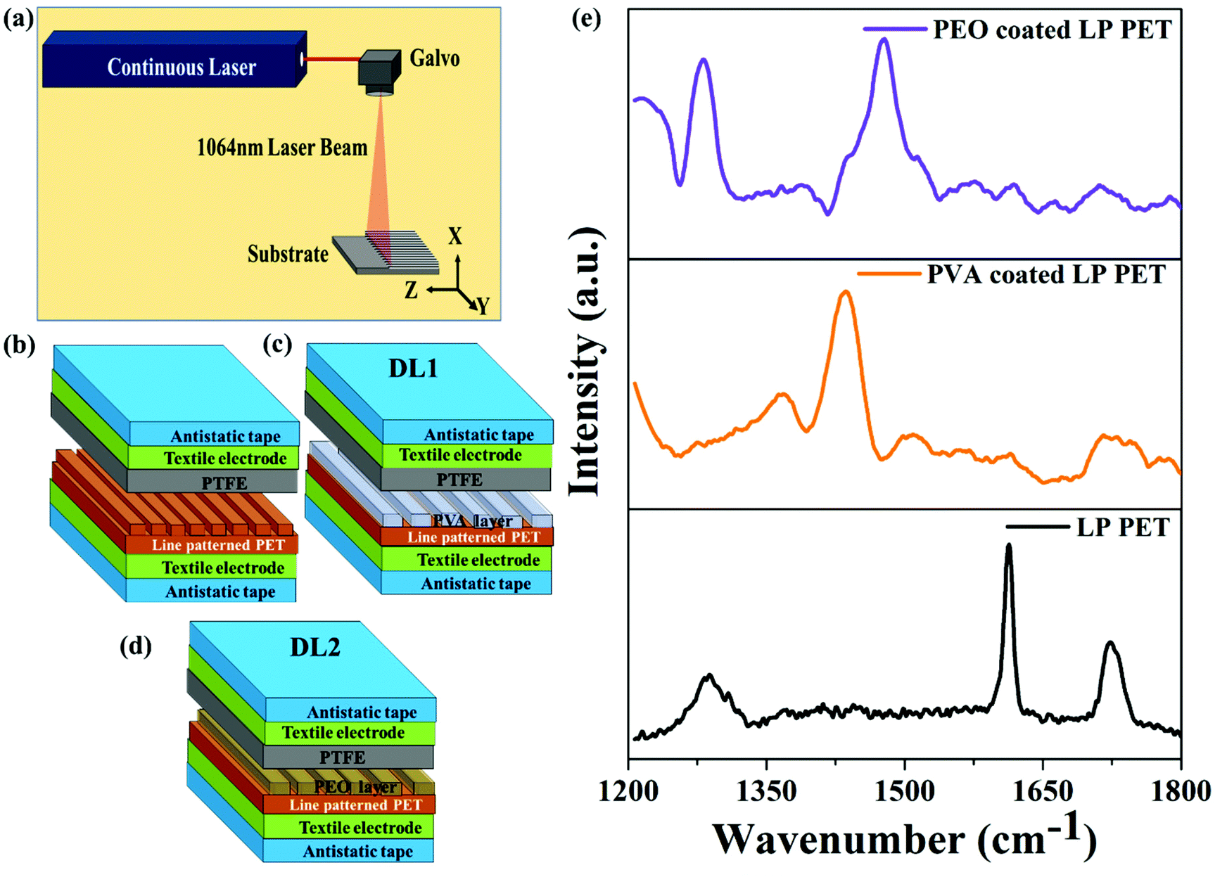 | ||
| Fig. 1 (a) Schematic diagram of laser processing (b) pristine LP-PTFE TENG device, (c) PVA coated LP-PTFE TENG, (d) PEO coated LP-PTFE TENG device, and (e) Raman shift before and after PEO/PVA coating of the LP PET surface. | ||
2.3 Characterization
The surface chemical modification of LP PET, DL1, and DL2 was analyzed by Raman spectroscopy with a 523 nm excitation wavelength. The as-fabricated TENG devices were characterized in the Dynamic fatigue failure system (Popwill Model YPS-1) for investigating the output performance with different mechanical parameters such as frequency (1–5 Hz), contact separation (CS) distance (2–12 mm), and mechanical force (10–70 N). A Femto/Pico ammeter (B2981A) was used to measure the current generated from the TENG devices. The series resistance of 110 MΩ was used across the device to measure the open-circuit voltage by an oscilloscope. The backside electrode of DL1 and DL2 devices was connected with a positive lead and the electrode of PTFE was the negative lead. The output measurement was carried out after the stabilized output, which was less than 100 cycles. Since, the PEO film is sensitive to humidity; a higher humidity affects the TENG performance. Hence, the whole experiments were carried out under the temperature of 25 °C and humidity of 35%.3. Results and discussion
The chemical modification and band stretching of pristine LP PET, DL1 and DL2 coated LP PET were analyzed by Raman spectroscopy (Fig. 1(e)). The carboxylic acid group and C![[double bond, length as m-dash]](https://www.rsc.org/images/entities/char_e001.gif) O bonds of the LP PET surface were confirmed and related to 1726 cm−1,39 but the peak intensities were reduced in the DL1 and DL2 layers due to –CH2CH2O– and –HOCHCH2-layers covered on the surface. It was observed that the PEO's CH2 groups are related to peaks at 1281 and 1479 cm−1 in the active Raman spectrum.48 However, at 1281 cm−1 the peak showed an increase which might be due to the amorphous part of the polymer chain.49 The oxygen group can donate an electron which increases the electrification of the device.50 In addition, the intermolecular interaction in the chemically modified LP PET and bare PET was analysed by FTIR and shown in Fig. S1.† There are four functional groups in the bare PET film: two esters, an aromatic ring, and an ethyl group. The terephthalate group is formed by combining the aromatic and two ester groups, and it contains different bonds such as C–C, C–H, C–O, CO, and aromatic rings (Table S1†). It was observed that laser-induced photophysical modification sharpened the ethyl and ester group peaks in the LP PET sample. Furthermore, at 1725 cm−1, a significant stretching vibration of CO was detected. Also, the strong and mild bending ethyl groups both showed up at 2970 and 731 cm−1, respectively. The transmittance intensity of the ethyl group increased due to a reduction in the concentration and oxygen may be expelled from the band which oxidizes the surface that improves the wettability and surface polarity.51 Another reason for the increase in intensity might be the thermal breakdown of PET chains and photo crosslinking between neighbouring chains.52 The TENG device's output is improved as a result of these surface modifications. The charge transport mechanism is explained in detail in the ESI section (S1).†
O bonds of the LP PET surface were confirmed and related to 1726 cm−1,39 but the peak intensities were reduced in the DL1 and DL2 layers due to –CH2CH2O– and –HOCHCH2-layers covered on the surface. It was observed that the PEO's CH2 groups are related to peaks at 1281 and 1479 cm−1 in the active Raman spectrum.48 However, at 1281 cm−1 the peak showed an increase which might be due to the amorphous part of the polymer chain.49 The oxygen group can donate an electron which increases the electrification of the device.50 In addition, the intermolecular interaction in the chemically modified LP PET and bare PET was analysed by FTIR and shown in Fig. S1.† There are four functional groups in the bare PET film: two esters, an aromatic ring, and an ethyl group. The terephthalate group is formed by combining the aromatic and two ester groups, and it contains different bonds such as C–C, C–H, C–O, CO, and aromatic rings (Table S1†). It was observed that laser-induced photophysical modification sharpened the ethyl and ester group peaks in the LP PET sample. Furthermore, at 1725 cm−1, a significant stretching vibration of CO was detected. Also, the strong and mild bending ethyl groups both showed up at 2970 and 731 cm−1, respectively. The transmittance intensity of the ethyl group increased due to a reduction in the concentration and oxygen may be expelled from the band which oxidizes the surface that improves the wettability and surface polarity.51 Another reason for the increase in intensity might be the thermal breakdown of PET chains and photo crosslinking between neighbouring chains.52 The TENG device's output is improved as a result of these surface modifications. The charge transport mechanism is explained in detail in the ESI section (S1).†
Fig. 2(a) and (b) show the vertical contact separation mechanism of a single and double dielectric layer coated TENG device model. The coupled effect of contact electrification and electrostatic induction is the basic phenomenon of the TENG mechanism.6,7 The conductive textile tape served as a top and bottom electrode of the device, over which the single and double electric layers were stacked. All the dielectric materials have dissimilar surface charge density, which assists to affirm the positive and negative charges of the TENG layer.36 When the force is imposed on top of the device, both dielectric layers come into contact with each other and transfer the charge from higher to lower electron affinity phases. However, when both layers are contact with each other, the electrons do not drive to the external circuit due to the electrical equilibrium state. When increasing the distance between two layers, the electric field drives the electrons from the top surface to the bottom electrode that leads to the negative current. When the device layers are close to each other for the next cycle, a reverse electrostatic potential is generated between the two surfaces, and that results in a positive current. The equation for the triboelectric field strength is derived from the Gaussian theorem (eqn (1) and (2)).44
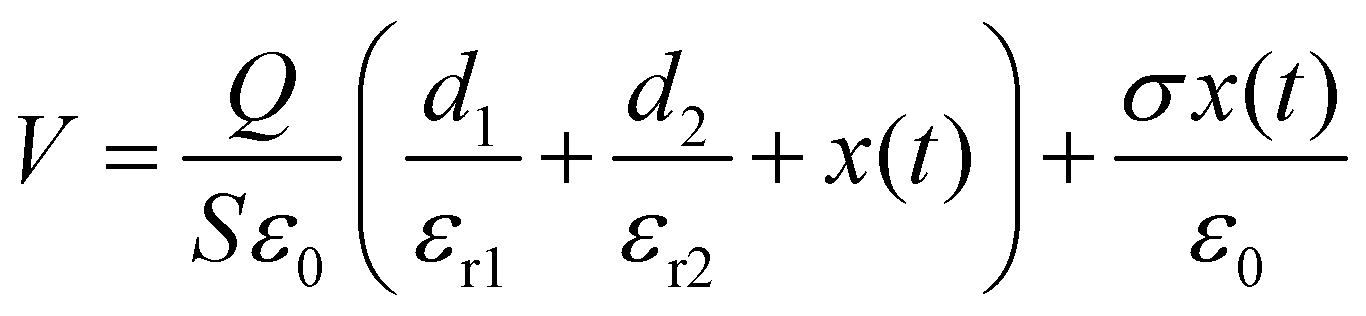 | (1) |
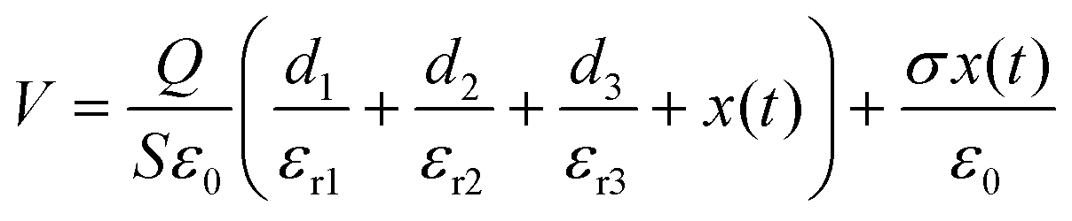 | (2) |
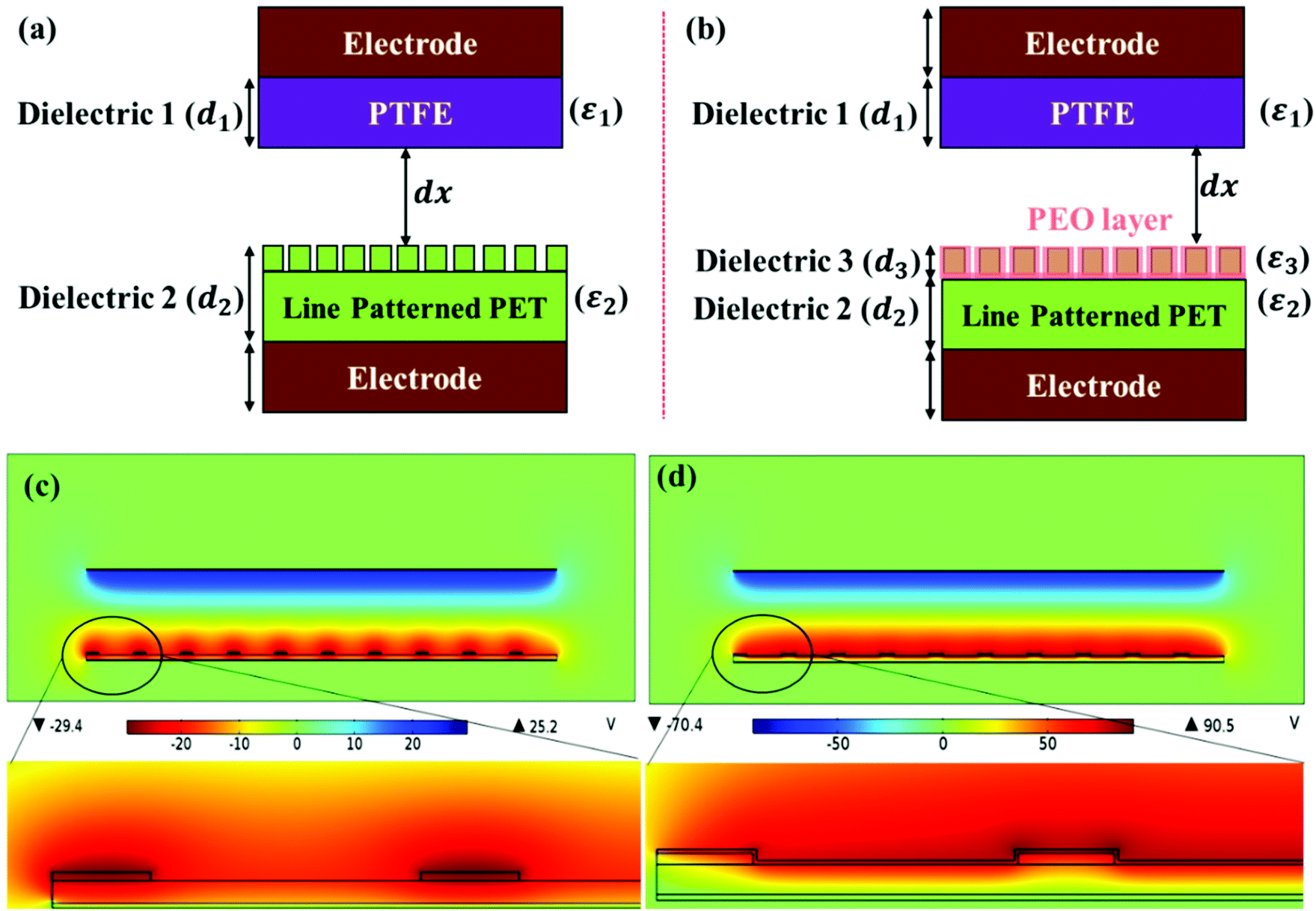 | ||
| Fig. 2 (a) and (b) Schematic diagram of single and DL2 TENG in the contact separation mode, (c) and (d) COMSOL Multiphysics simulation of pristine and the PEO coated LP PET TENG device. | ||
To investigate the triboelectric performance of the pristine LP PET surface and interfacial polymer coated-LP PET surface, we have designed the TENG structures and simulated them in the COMSOL Multiphysics software with contact separation mode. Fig. 2(c) and (d) depict the voltage generation between the two different TENG devices such as the PTFE with pristine LP PET device and the PTFE with DL2 device. Among them, the PTFE with DL2 device has generated a higher voltage compared to the former. The inset image shows the before and after PEO coating of pristine LP PET. It has been observed that no voltage was generated (Fig. S2†) when mechanical force is imposed on the device due to electrical equilibrium conditions. Once the mechanical force is released from the device, the electric field builds up and drives the electrons from one side to the other side. Hence, the PTFE with DL2 device attains higher performance than the pristine device.
The triboelectric output performance was evaluated for the pristine LP TENG and DL1 and DL2 TENG by the contact separation mechanism. These devices were initially deployed with a force of 50 N, frequency of 4 Hz, and CS distance of 4 mm for measuring the open circuit (Voc) voltage and short circuit current (Isc). Fig. 3(a) depicts the FESEM image of DL2 coated LP PET and the inset image shows the digital photos of the dielectric coated PET with/without the electrode. The transferred charge was measured for the single, DL1 and DL2 TENG (Fig. 3(b)), in which the DL2 TENG device (13.8 nC) transferred more charges compared to other devices. Such high performance is attributed to the higher surface contact area as well improved interfacial area between the LP PET and PEO which promotes charge accumulation53,60 and thus enhanced transferred charges.
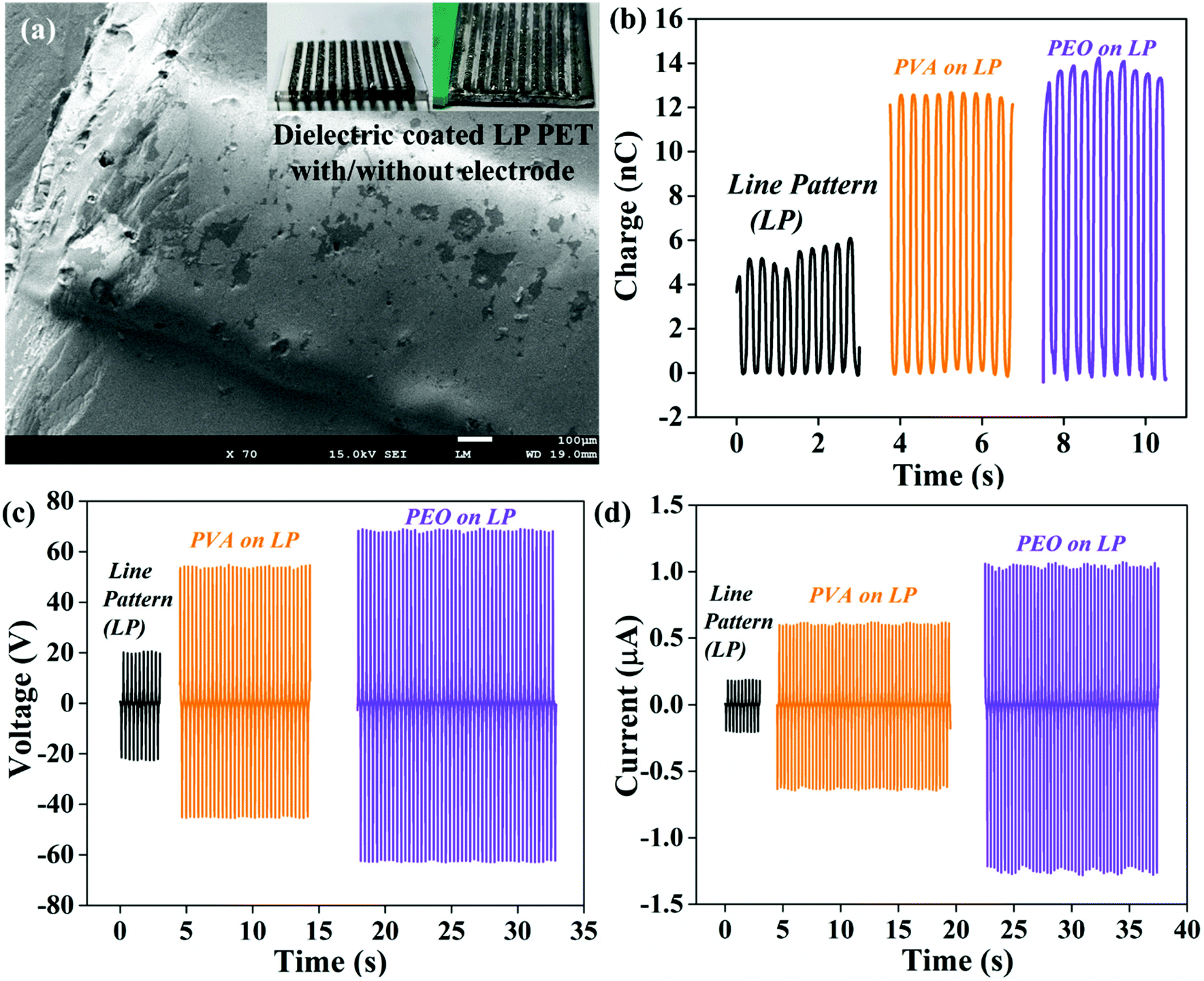 | ||
| Fig. 3 (a) Photographic image of the dielectric coated with and without electrode LP PET (b) transfer charges of single and double-layered TENG (c) and (d) Voc and Isc measurement of DL1 and DL2 TENG devices with the fixed operational parameters i.e., frequency of 5 Hz, CS distance 4 mm, and a force of 50 N. | ||
Fig. 3(c) and (d) depict the Voc and Isc of single, DL1 and DL2 TENG devices. The single-layer TENG device generated a peak-to-peak (PP) Voc of 42.65 V and Isc of 0.485 μA at a load resistance of 110 MΩ. The DL2 device generated a peak to peak Voc of 131.85 V and Isc of 2.327 μA. The DL2 device exhibited 2-fold higher performance than single-layer TENG device. The comprehensive results are tabulated in Table S2.† It is due to more charge accumulation and a higher tendency to trap more charges between LP PET and the PEO layer, owing to its lower electron affinity and the unique PEO chains, such as –C–, –O–, and – H–, which repelled electrons from its surface by the electrostatic effect.54 This property substantially aids in improving the triboelectrification process of the device. Also, the larger surface contact area is one of the inevitable factors to enhance its output performance. Compared to our previous work,42 the present study improves the output performance by 4-fold by the effect of the PEO layer as well larger surface contact area. For further investigations, PEO-coated LP TENG has been used.
It is essential to examine the DL2 device performance with various mechanical parameters such as mechanical force, frequency, contact separation distance, and load resistance. Fig. 4(a) and (b) depict the Voc and Isc of the DL2 TENG device at different frequencies of 1–5 Hz, fixed force, and CS distance of 50 N and 4 mm with 110 MΩ resistance. Lower Voc (85.69 V) and Isc (0.782 μA) were generated at 1 Hz. However, the device exhibited higher output (161.16 V, 2.466 μA) at a frequency of 5 Hz. The output performance was considerably increased by increasing the frequency. More tapping induced faster electron flow between the surfaces.55 Based on the following equation, the output performance under various frequency conditions has been analyzed.
 | (3) |
 | (4) |
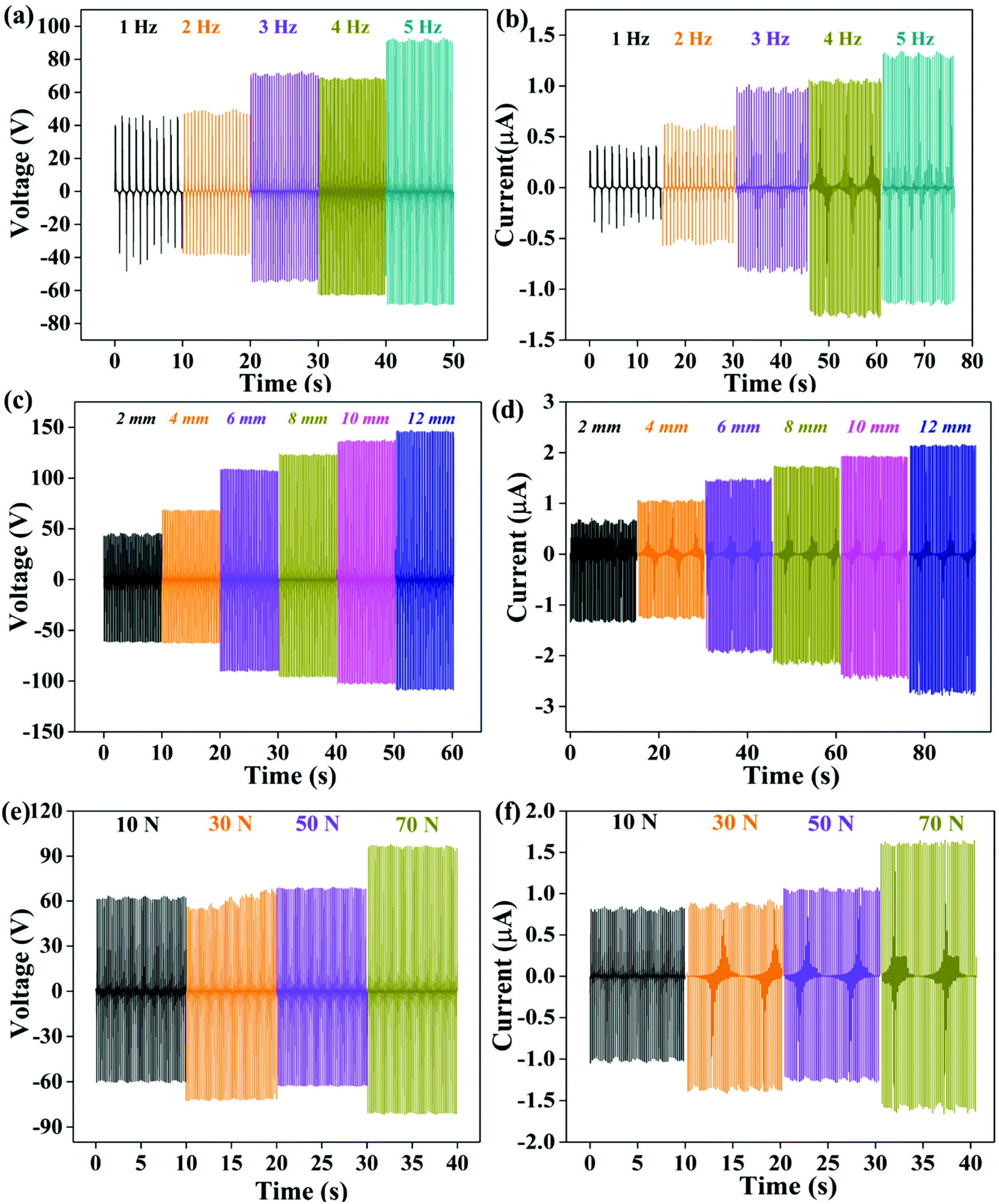 | ||
| Fig. 4 (a) and (b) Voc and Isc of DL1/DL2 TENG with various frequencies (1–5 Hz); CS distance and load were fixed at 4 mm, and 50 N, (c) and (d) Voc and Isc evaluation under different CS distances (2 to 12 mm) with a constant load of 50 N and frequency of 4 Hz, (e) and (f) shows the performance of Voc and Isc for different contact forces (10–70 N) with a constant frequency and CS distance (4 Hz and 4 mm). | ||
The device's functional ability is determined by the contact separation distance. So, the fabricated device was deployed at various CS distances from 2–12 mm with an interval of 2 mm, a frequency of 4 Hz, and a fixed load of 50 N shown in Fig. 4(c) and (d). Due to the weaker electric field generated between the two surfaces, the smaller CS distance resulted in a low Isc of 2.0494 μA and Voc of 107.42 V. At the larger CS distance (12 mm), the DL2 device has obtained a notable output Voc of 254 V and Isc of 4.848 μA compared to other distances. According to eqn (3), the larger contact separation distance improves relative contact velocity which leads to drive the electron flow very fast.43,47 Above a certain distance, the system performance gets slowly saturated.
Mechanical force is a vital parameter that assists to correlate the effective contact area with induced charges. Hence, the DL2 TENG device performance was investigated thoroughly with various contact forces from 10 N to 70 N and it is depicted in Fig. 4(e) and (f). It is observed that the lower contact force of 10 N yields a smaller potential of 123.08 V and Isc of 1.864 μA. The output range progressively improved (123.08 to 178.25 V) as the contact force was increased from 10 N to 70 N. At the higher level of contact force, the PTFE layer completely contacts each corner of the DL2 surface due to being elastic in nature. The higher contact area has more interaction between the two subjected dielectric layers which increases the kinetic energy of electron transfer.55,56,59
The endurance of a mechanical energy harvesting system is essential for assessing its stability and reliability. The DL2 TENG device was operated for 10000 cycles at 4 Hz frequency, 50 N mechanical force, and 4 mm CS distance (Fig. 5(a)). In the graph, the last 500 cycles of each consecutive 1000 cycles has been plotted (1–500, 1501–2000, 2501–3000…). The device exhibits excellent mechanical robustness without any notable deterioration in the Isc. The various load resistances (1 kΩ to 4 GΩ) were used for maximum output voltage and Isc drop as shown in Fig. 5(b). The Voc gradually increased from 0 to 363.72 V as the load resistance increased and saturated after 1 GΩ but the Isc was reversed, and, due to the higher resistance, the current flow decreased drastically beyond 110 MΩ. The output power density was estimated using eqn (5).
 | (5) |
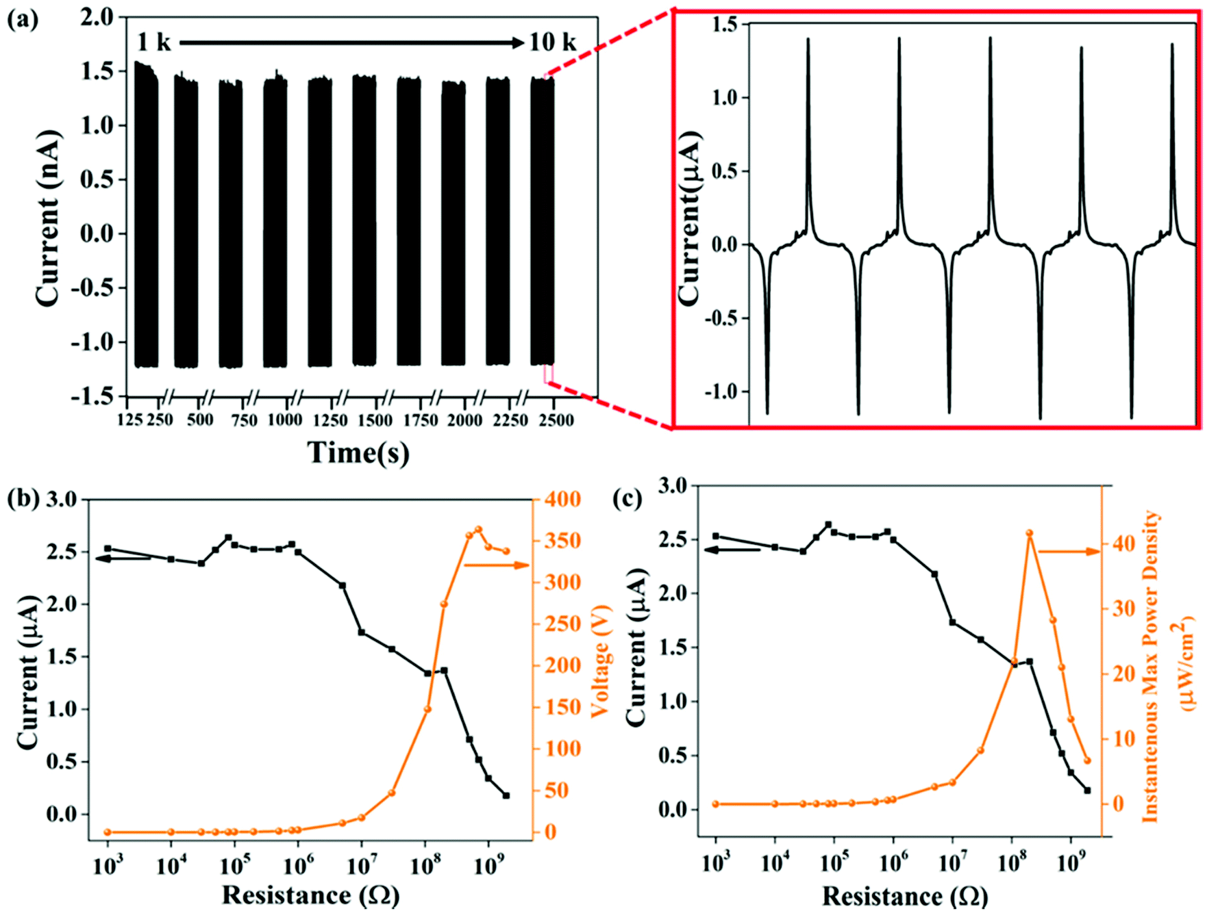 | ||
| Fig. 5 (a) Endurance evaluation of Isc for the DL2 device operated up to 10000 cycles with a force of 50 N, frequency of 4 Hz, and CS distance of 4 mm; the inset images show that performance at the middle of the endurance operation evaluation and peak degradation analysis. (b) Voc and Isc across the different load resistance, and (c) Instantaneous max power density measurement with the different load resistance. | ||
Also, eqn (5) was used to appraise the instantaneous max power density and Isc drop (Fig. 5(c)). The power density steadily increased when the load resistance increased from 1 kΩ to 110 MΩ. The maximum power density of 41.6 μW cm−2 was obtained at 110 MΩ load resistance. Hence, this maximum power density can be used to power up the microsensors and low-power electronic devices.3,27,33
Furthermore, Fig. 6(b) depicts the storage capability of the DL2 device in which the generated energy is stored in three different capacitors (0.1 μF, 2.2 μF, and 22 μF) with a length of 40 s by using the external circuit connection (Fig. 6(a)). It is observed that the device charged a maximum of 5 V with a small capacitance of 0.1 μF at 40 s, and in the case of higher capacitance it required more time to store maximum voltage. Fig. 6(c) shows the energy stored in various commercial capacitors and the 2.2 μF capacitor stored the maximum energy of 1.73 μJ within a short period than the others. It is noticed that increasing the capacitance will increase the time for charging and discharging, hence the optimal capacitance (2.2 μF) will be appropriate. The charged capacitor was deployed to light ten LEDs with high intensity and is shown in Fig. 6(d). Thus, the DL2 device can power up micro and nanoelectronic devices.
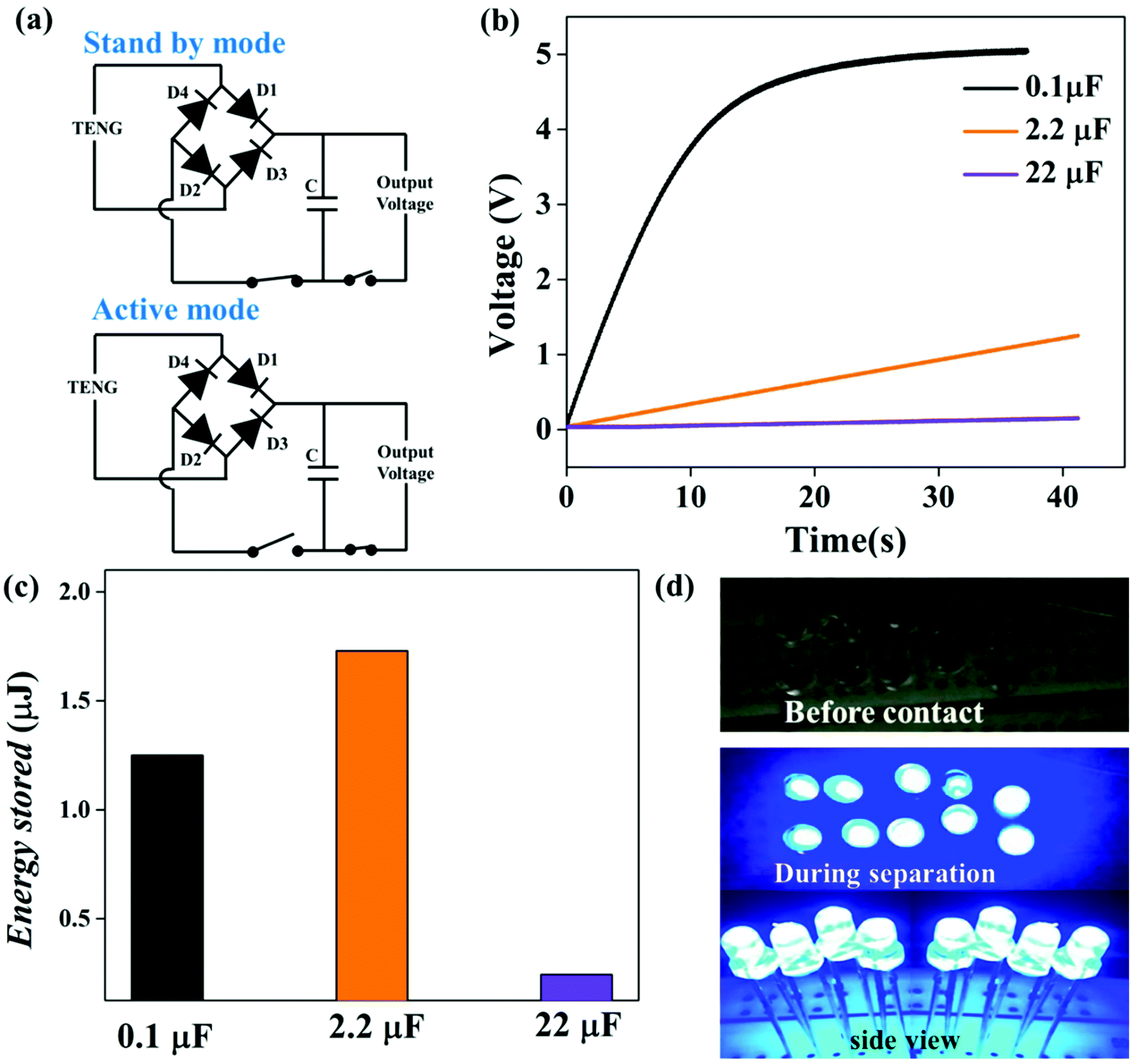 | ||
| Fig. 6 Schematic diagram of the charging circuit (a) and (b) the DL2 device deployed to generate the voltage stored in different capacitors, (c) the amount of energy stored in various capacitors, and (d) the digital image of ten LEDs lighten up by charged capacitor. | ||
4. Conclusion
Single and two different double layer (DL1, DL2) coated LP TENG devices were demonstrated to boost the triboelectric output performance. The DL2 device exhibited higher performance than the DL1 and single-layer device due to the enhanced interfacial area and surface contact area. Subsequently, the triboelectric behaviours were thoroughly investigated with different mechanical parameters such as mechanical force (10–70 N), frequency (1–5 Hz), CS distance (2–12 mm), and load resistance (1000–4 GΩ). The optimized mechanical parameters resulted in a higher output voltage, current, and instantaneous power density of 131 V and 2.32 μA, 41.6 W cm−2 for the DL2 device (4 Hz, 4 mm, and 50 N). The performance was enhanced 2-fold for the single layer TENG device and 4-fold for the DL2 device compared to the PA6-laser patterned PET TENG device (our previous report), which satisfies the motivation of this work. Additionally, the DL2 device endurance was evaluated for 10000 cycles which shows no negligible degradation. Also, ten LEDs that were serially connected glowed with the charged capacitor. Hence, the PEO coated LP TENG device will be suitable for powering micro and nano-electronic devices.
Author contributions
Manikandan Muthu: Conceptualization, data curation, writing – review and editing, writing – original draft, investigation, formal analysis, methodology, software, validation, visualization, funding acquisition. Rajagopalan Pandey: Investigation, formal analysis, methodology, writing – review and editing. Shujia Xu: Software, visualization. Palani IA: Project administration, resources, supervision, validation. Vipul Singh: Supervision, validation. Xiaozhi Wang: Resources, formal analysis, validation. Wenzhuo Wu: Formal analysis, validation.Conflicts of interest
There are no conflicts of interest to declare.Acknowledgements
Manikandan M would like to express his gratitude to SERB India (SB/S9/Z-03/2017-XIV (2019-20)) for the fellowship from the India-Purdue OVDF Program. MM is thankful to Zhejiang University's Department of Information Science and Electronic Science for providing the characterization facility. MM would like to thank the mechatronics and instrumentation group, the molecular nano research group, and Mr Sarathkumar K of IIT Indore for his valuable discussion. Also, MM is thankful to Prof Wu's research group for their valuable discussion.References
- Y. Yang, L. Lin, Y. Zhang, Q. Jing, T. C. Hou and Z. L. Wang, ACS Nano, 2012, 6(11), 10378–10383 CrossRef CAS PubMed.
- J. Zhao, R. Ghannam, K. O. Htet, Y. Liu, M. K. Law, V. A. Roy, B. Michel, M. A. Imran and H. Heidari, Adv. Healthcare Mater., 2020, 9(17), 2000779 CrossRef CAS PubMed.
- A. Nozariasbmarz, H. Collins, K. Dsouza, M. H. Polash, M. Hosseini, M. Hyland, J. Liu, A. Malhotra, F. M. Ortiz, F. Mohaddes and V. P. Ramesh, Appl. Energy, 2020, 258, 114069 CrossRef.
- M. Manikandan, P. Rajagopalan, N. Patra, S. Jayachandran, M. Muralidharan, S. M. Prabu, I. A. Palani and V. Singh, Nanotechnology, 2020, 31(18), 185401 CrossRef CAS PubMed.
- R. Pandey, G. Khandelwal, I. A. Palani, V. Singh and S. J. Kim, Nanoscale, 2019, 11(29), 14032–14041 RSC.
- P. Rajagopalan, S. Huang, L. Shi, H. Kuang, H. Jin, S. Dong, W. Shi, X. Wang and J. Luo, Nano Energy, 2021, 80, 105560 CrossRef CAS.
- F. R. Fan, Z. Q. Tian and Z. L. Wang, Nano Energy, 2012, 1(2), 328–334 CrossRef CAS.
- S. Xu and W. Wu, Adv. Intell. Syst., 2020, 2(10), 2000117 CrossRef.
- X. Chen, Y. Wu, J. Shao, T. Jiang, A. Yu, L. Xu and Z. L. Wang, Small, 2017, 13(47), 1702929 CrossRef PubMed.
- Y. S. Zhou, G. Zhu, S. Niu, Y. Liu, P. Bai, Q. Jing and Z. L. Wang, Adv. Mater., 2014, 26(11), 1719–1724 CrossRef CAS PubMed.
- Y. Wang, H. Wu, L. Xu, H. Zhang, Y. Yang and Z. L. Wang, Sci. Adv., 2020, 6(34), eabb9083 CrossRef CAS PubMed.
- R. Wang, L. Mu, Y. Bao, H. Lin, T. Ji, Y. Shi, J. Zhu and W. Wu, Adv. Mater., 2020, 32(32), 2002878 CrossRef CAS PubMed.
- R. D. I. G. Dharmasena and S. R. P. Silva, Nano Energy, 2019, 62, 530–549 CrossRef CAS.
- Z. Xie, J. Dong, F. Yang, R. Xu, Q. Gao, T. Cheng and Z. L. Wang, Extreme Mech. Lett., 2020, 37, 100713 CrossRef.
- C. Wu, A. C. Wang, W. Ding, H. Guo and Z. L. Wang, Adv. Energy Mater., 2019, 9(1), 1802906 CrossRef.
- Y. Long, Y. Chen, Y. Liu, G. Chen, W. Guo, X. Kang, X. Pu, W. Hu and Z. L. Wang, Nanoscale, 2020, 12(24), 12753–12759 RSC.
- Y. Xie, Q. Ma, H. Qi, X. Liu, X. Chen, Y. Jin, D. Li, W. Yu and X. Dong, Nanoscale, 2021, 13, 19144–19154 RSC.
- S. Fu, W. He, Q. Tang, Z. Wang, W. Liu, Q. Li, C. Shan, L. Long, C. Hu and H. Liu, Adv. Mater., 2021, 2105882 CrossRef PubMed.
- Y. Yu and X. Wang, Extreme Mech. Lett., 2016, 9, 514–530 CrossRef.
- X. S. Zhang, M. D. Han, B. Meng and H. X. Zhang, Nano Energy, 2015, 11, 304–322 CrossRef CAS.
- L. Lin, S. Wang, Y. Xie, Q. Jing, S. Niu, Y. Hu and Z. L. Wang, Nano Lett., 2013, 13(6), 2916–2923 CrossRef CAS PubMed.
- I. Kim, H. Roh, W. Choi and D. Kim, Nanoscale, 2021, 13(19), 8837–8847 RSC.
- S. W. Chen, X. Cao, N. Wang, L. Ma, H. R. Zhu, M. Willander, Y. Jie and Z. L. Wang, Adv. Energy Mater., 2017, 7(1), 1601255 CrossRef.
- Y. Ra, J. H. Choi, S. J. Choi, M. La, S. J. Park, M. J. Kim and D. Choi, Extreme Mech. Lett., 2020, 40, 100910 CrossRef.
- L. Lin, S. Wang, S. Niu, C. Liu, Y. Xie and Z. L. Wang, ACS Appl. Mater. Interfaces, 2014, 6(4), 3031–3038 CrossRef CAS PubMed.
- M. G. Stanford, J. T. Li, Y. Chyan, Z. Wang, W. Wang and J. M. Tour, ACS Nano, 2019, 13(6), 7166–7174 CrossRef CAS PubMed.
- C. K. Chung and K. H. Ke, Appl. Surf. Sci., 2020, 508, 145310 CrossRef CAS.
- H. Phan, P. N. Hoa, H. A. Tam, P. D. Thang and N. H. Duc, Extreme Mech. Lett., 2020, 40, 100886 CrossRef.
- R. Wang, S. Gao, Z. Yang, Y. Li, W. Chen, B. Wu and W. Wu, Adv. Mater., 2018, 30(11), 1706267 CrossRef PubMed.
- Y. Chen, B. Xie, J. Long, Y. Kuang, X. Chen, M. Hou, J. Gao, S. Zhou, B. Fan, Y. He and Y. T. Zhang, Adv. Mater., 2021, 2104290 CrossRef CAS PubMed.
- X. S. Zhang, M. D. Han, R. X. Wang, F. Y. Zhu, Z. H. Li, W. Wang and H. X. Zhang, Nano Lett., 2013, 13(3), 1168–1172 CrossRef CAS PubMed.
- Y. Hu, X. Wang, H. Li, H. Li and Z. Li, Nano Energy, 2020, 71, 104640 CrossRef CAS.
- F. R. Fan, L. Lin, G. Zhu, W. Wu, R. Zhang and Z. L. Wang, Nano Lett., 2012, 12(6), 3109–3114 CrossRef CAS PubMed.
- V. T. Bui, Q. Zhou, J. N. Kim, J. H. Oh, K. W. Han, H. S. Choi, S. W. Kim and I. K. Oh, Adv. Funct. Mater., 2019, 29(28), 1901638 CrossRef.
- A. R. Mule, B. Dudem and J. S. Yu, Energy, 2018, 165, 677–684 CrossRef CAS.
- A. Chen, C. Zhang, G. Zhu and Z. L. Wang, Adv. Sci., 2020, 7(14), 2000186 CrossRef CAS PubMed.
- Y. Zhou, M. Shen, X. Cui, Y. Shao, L. Li and Y. Zhang, Nano Energy, 2021, 105887 CrossRef CAS.
- W. He, X. Fu, D. Zhang, Q. Zhang, K. Zhuo, Z. Yuan and R. Ma, Nano Energy, 2021, 2021, 105880 CrossRef.
- H. S. Wang, C. K. Jeong, M. H. Seo, D. J. Joe, J. H. Han, J. B. Yoon and K. J. Lee, Nano Energy, 2017, 35, 415–423 CrossRef CAS.
- Y. H. Kwon, S. H. Shin, J. Y. Jung and J. Nah, Nanotechnology, 2016, 27(20), 205401 CrossRef PubMed.
- S. H. Shin, D. Park, J. Y. Jung, P. Park and J. Nah, Nanoscale, 2018, 10(45), 20995–21000 RSC.
- V. Raman, J. Jo and H. K. Kim, Mater. Sci. Semicond. Process., 2020, 120, 105277 CrossRef CAS.
- M. Muthu, R. Pandey, X. Wang, A. Chandrasekhar, I. A. Palani and V. Singh, Nano Energy, 2020, 78, 105205 CrossRef CAS.
- J. J. Shao, W. Tang, T. Jiang, X. Y. Chen, L. Xu, B. D. Chen, T. Zhou, C. R. Deng and Z. L. Wang, Nanoscale, 2017, 9(27), 9668–9675 RSC.
- N. Cui, J. Liu, Y. Lei, L. Gu, Q. Xu, S. Liu and Y. Qin, ACS Appl. Energy Mater., 2018, 1(6), 2891–2897 CrossRef CAS.
- J. Chun, B. U. Ye, J. W. Lee, D. Choi, C. Y. Kang, S. W. Kim, Z. L. Wang and J. M. Baik, Nat. Commun., 2016, 7(1), 1–9 Search PubMed.
- P. Ding, J. Chen, U. Farooq, P. Zhao, N. Soin, L. Yu, H. Jin, X. Wang, S. Dong and J. Luo, Nano Energy, 2018, 46, 63–72 CrossRef CAS.
- A. Kotzianova, J. Rebicek, O. Zidek, M. Pokorny, J. Hrbac and V. Velebny, Anal. Methods, 2015, 7(23), 9900–9905 RSC.
- I. S. Elashmawi and L. H. Gaabour, Results Phys., 2015, 5, 105–110 CrossRef , 3.
- A. Chen, C. Zhang, G. Zhu and Z. L. Wang, Adv. Sci., 2020, 7(14), 2000186 CrossRef CAS PubMed.
- A. A. El-Saftawy, A. Elfalaky, M. S. Ragheb and S. G. Zakhary, Radiat. Phys. Chem., 2014, 102, 96–102 CrossRef CAS.
- M. A. Fadel, N. A. Kamel, M. M. Darwish, S. L. Abd El-Messieh, K. N. Abd-El-Nour and W. A. Khalil, Prog. Biomater., 2020, 9(3), 107–114 CrossRef CAS PubMed.
- D. Yoo, E. Y. Go, D. Choi, J. W. Lee, I. Song, J. Y. Sim, W. Hwang and D. S. Kim, Nanomaterials, 2019, 9(1), 71 CrossRef PubMed.
- J. M. Wu, Y. H. Lin and B. Z. Yang, Nano Energy, 2016, 22, 468–474 CrossRef CAS.
- R. Pan, W. Xuan, J. Chen, S. Dong, H. Jin, X. Wang, H. Li and J. Luo, Nano Energy, 2018, 45, 193–202 CrossRef CAS.
- M. L. Seol, S. H. Lee, J. W. Han, D. Kim, G. H. Cho and Y. K. Choi, Nano Energy, 2015, 17, 63–71 CrossRef CAS.
- J. Xiong, P. Cui, X. Chen, J. Wang, K. Parida, M. F. Lin and P. S. Lee, Nat. Commun., 2018, 9(1), 1–9 CrossRef PubMed.
- M. Zhang, L. Xia, S. Dang, L. Shi, A. Cao, Q. Deng and C. Du, AIP Adv., 2019, 9(7), 075221 CrossRef.
- A. Chandrasekhar, N. R. Alluri, M. S. P. Sudhakaran, Y. S. Mok and S. J. Kim, Nanoscale, 2017, 9(28), 9818–9824 RSC.
- D. W. Kim, J. H. Lee, J. K. Kim and U. Jeong, NPG Asia Mater., 2020, 12(1), 1–17 CrossRef.
Footnote |
| † Electronic supplementary information (ESI) available. See DOI: 10.1039/d1nr07021e |
| This journal is © The Royal Society of Chemistry 2021 |