
Electronic and magnetic properties of n-type and p-doped MoS2 monolayers
Xu Zhao*a,
Peng Chena,
Congxin Xiaa,
Tianxing Wang*a and
Xianqi Daiab
aCollege of Physics and Electronic Engineering, Henan Normal University, Xinxiang, Henan 453007, China. E-mail: zhaoxu@htu.cn; wtxdd@163.com
bDepartment of Physics, Zhengzhou Normal University, Zhengzhou, Henan 450044, China
First published on 2nd February 2016
Abstract
The electronic and magnetic properties of n- and p-type impurities by means of group V and VII atoms substituting sulfur in a MoS2 monolayer were investigated using first-principles methods based on density functional theory. Numerical results show that group V and VII atoms can induce magnetic properties, and the magnetic moment mainly originates from the dopant’s p orbital and neighbor Mo atoms’ d orbital. N-, P-, F-, and I-doped (or As-doped) MoS2 exhibits magnetic nanomaterial (or metallic) features, and Cl- and Br-doped systems exhibit half-metallic ferromagnetism (HMF). Moreover, the formation energy calculations also indicate that it is energetically favorable and relatively easier to incorporate group V and VII atoms into a MoS2 monolayer under Mo-rich experimental conditions. The formation energy of the F-doped system is the lowest, the next lowest formation energy is obtained in the Cl-doped system. By comparison, Cl-doped MoS2 is more suitable for spin injection. This finding is important for the achievement of spin devices on MoS2 nanostructures.
I. Introduction
Transition metal dichalcogenides (TMDs), with the chemical formula MX2 (M = Ti, Zr, Hf, V, Nb, Ta, Cr, Mo, and W, X = S, Se and Te), have been extensively studied. Layered semiconductor TMDs have proven to be important candidates for use as an absorber layer in low cost thin film solar cells.1 This is due to their relatively small band gap (∼1–2 eV) and large absorption coefficient.2 In particular, MoS2 has been steadily attracting more attention. Recently, possible applications, including transistors,3,4 photoemitting devices,5 photovoltaics,6 catalysis,7 hydrogen storage,8 lubricants,9 and Li-ion batteries10 have been proposed and investigated. Great attention has been paid to the exploration of the magnetic properties of transition-metal dichalcogenides for nanoscale spintronic devices. As is well-known, spintronic devices play an important role in their promising application in information technologies.11,12 Highly spin-polarized ferromagnetism, especially half-metallic ferromagnetism (HMF) is a key ingredient for future high-performance spintronic devices.13–15 HMF, where one spin direction behaves like a metal and the other is semiconducting were first predicted.16 Thus far, HMF has been found in different types of materials, such as pure organic compounds,17 organic–inorganic hybrid compounds,18 transition-metal oxides,19 transition-metal pnictides and chalcogenides,20 Heusler alloys,21,22 and zincblende compounds.23,24 Dilute magnetic semiconductors (DMSs) with half-metallicity have been extensively studied due to their carrier-mediated ferromagnetism, which makes them ideal for spintronics applications by offering the possibility of electronic control of magnetism.25,26 Manifestation of the ferromagnetic (FM) phase has been done with various treatments: vacancy-defect formation,27–29 nanoribbon with zigzag edges,30–33 and adsorption or substitution of a transition metal.34–38 Transition-metal-doped semiconductors have been the subject of investigations for possible spintronics applications.39–43 In particular, some groups have reported that intrinsic nonmagnetic elements such as dopants can produce HMF in some semiconductors.29,44–50 While, the systematic study of the electronic and magnetic characteristics of n- and p-type impurities by means of group V and VII atoms substituting sulfur in a MoS2 monolayer so far is still limited. In this paper, we investigate the structural, electronic and magnetic properties of (V, VII)-doped MoS2, using first-principles calculations, which may find promising applications in spintronics devices.The paper is organized as follows. In Sec. II we give an overview on the theoretical methods used in the work. In Sec. III we investigate the electronic and magnetic properties of (V, VII)-doped MoS2 using first-principle calculations, we find that group V and VII atoms can induce magnetic properties, N-, P-, F-, and I-doped (or As-doped) MoS2 exhibits magnetic nanomaterial (or metallic) features, Cl- and Br-doped MoS2 exhibits half-metallic ferromagnetism (HMF) and the half-metallic gap is about 0.115 and 0.081 eV, respectively. The Cl-doped system is suitable for spin injection. Section IV summarizes the work.
II. Theoretical models and methods
Bulk MoS2 is an indirect gap semiconductor, with a gap of ∼1.3 eV,51,52 while as the material transitions to a monolayer the gap becomes direct with size ∼1.8 eV.53,54 Layered MoS2 consists of stacked S–Mo–S layers. MoS2 layers have a P63/mmc space group symmetry with the Mo atoms having a trigonal prismatic coordination with the S atoms, as shown in Fig. 1. The bonds within the trilayers are covalent, adjacent layers are held together by weak van der Waals forces, enabling the well-known method of mechanical exfoliation. Thus, one can cleave the material down to single layer thickness.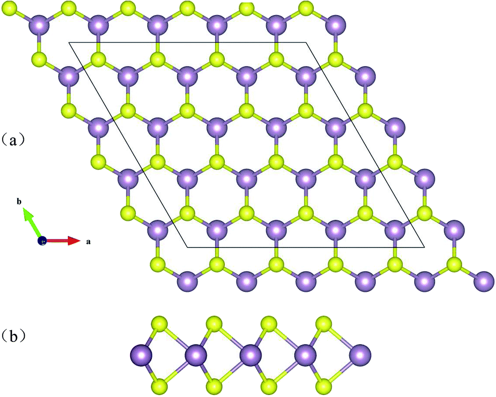 | ||
| Fig. 1 Schematic structure of MoS2. The top and side views of the layered forms are shown. The purple and yellow balls represent Mo and S atoms, respectively. | ||
Our calculations were performed within first-principles DFT using the projector augmented wave (PAW) method55 within the Vienna ab initio simulation package (VASP).56 Electron exchange and correlation effects were described within the generalized gradient approximation (GGA) in the Perdew–Burke–Ernzerhof (PBE) parametrization.57 In all calculations, an energy cutoff of 500 eV for the plane-wave expansion of the wavefunctions was used. The valence electron configuration was S (3s2p4), Mo(4d55s1), N(2s2p3), P(3s2p3), As(4s2p3), F(2s2p5), Cl(3s2p5), Br(4s2p5) and I(5s2p5). The Brillouin-zone integrations were performed using special k-point sampling of the Monhkorst–Pack scheme. The k-points 9 × 9 × 1 were used for the two-dimensional 4 × 4 × 1 MoS2 supercell. In order to avoid any artificial interaction between neighboring images, the vacuum layer along the z-direction was at least 15 Å for the MoS2 supercell. All the structures were fully relaxed to minimize the total energy of the systems until a precision of 10−5 was reached. Both the atomic positions and cell parameters were optimized until the residual forces fell below 0.01 eV/Å.
III. Results and discussion
In this work, we investigate firstly the structural and electronic properties of the X-doped MoS2 monolayer. The calculated Mo–X binding length (X denotes group V and VII atoms), dMo–X, magnetic moment, MMo, MX, Mtot, total energy of the doped system, Edoped and the formation energy in different experimental conditions, Eform, are listed in Table 1. It can be seen that dMo–X, except for dMo–N, dMo–P and dMo–F, is more than dMo–S (2.407 Å), indicating a covalent-bond interaction between the Mo and X atoms. As the atomic size increases, dMo–X increases from N to As (or from F to I). The shortest dMo–X of 2.015 Å was found for a N impurity. We can also see from Table 1 that the total energy of the N-doped MoS2 case is lowest, which indicates that the N-doped MoS2 monolayer is much more stable than the other considered impurity cases. Our calculations demonstrate that a magnetic moment was observed for group V and VII atom substitution, and the total magnetic moment of the As-doped system was the smallest (0.053 μB) of those studied. However, the magnetic moment of all X-doped systems was less than 1 μB.| System | dX–Mo1 (Å) | dX–Mo2 (Å) | dX–Mo3 (Å) | MMo1 (μB) | MMo2 (μB) | MMo3 (μB) | X (μB) | Mtot (μB) | Edoped (eV) | Eform (eV) | |
|---|---|---|---|---|---|---|---|---|---|---|---|
| Mo-rich | S-rich | ||||||||||
| N | 2.015 | 2.015 | 2.015 | 0.034 | 0.034 | 0.034 | 0.231 | 0.779 | −351.04 | 0.574 | 2.02 |
| P | 2.387 | 2.387 | 2.389 | 0.094 | 0.089 | 0.093 | 0.169 | 0.72 | −348.06 | 1.312 | 2.758 |
| As | 2.58 | 2.58 | 2.595 | 0.002 | 0.002 | 0.018 | 0.007 | 0.053 | −347.24 | 4.184 | 5.63 |
| F | 2.364 | 2.364 | 2.154 | 0.294 | 0.301 | 0.081 | 0.066 | 0.853 | −346.82 | −1.469 | −0.023 |
| Cl | 2.573 | 2.573 | 2.495 | 0.321 | 0.334 | 0.09 | 0.061 | 0.863 | −345.07 | 0.216 | 1.662 |
| Br | 2.674 | 2.674 | 2.683 | 0.223 | 0.25 | 0.261 | 0.068 | 0.857 | −344.38 | 1.058 | 2.504 |
| I | 2.824 | 2.824 | 3.004 | 0.115 | 0.115 | 0.485 | 0.074 | 0.823 | −343.79 | 1.542 | 2.988 |
To probe the stability of the X-doped MoS2 monolayer, the formation energy Eform can be calculated according to the following formula58–62
| Eform = E(doped) − E(pure) + n(μS − μX). | (1) |
| 2μS + μMo = μMoS2 | (2) |
Next, we studied the electronic structures of the X-doped MoS2 monolayer. Fig. 2 illustrates the results of the band structure for the pristine and X-doped MoS2 monolayer. For the pristine monolayer MoS2 4 × 4 supercell, the direct band gap at the k-point is estimated to be Eg = 1.80 eV, which is very consistent with that of the primitive cell calculation.53,54 Compared with the pristine case, flat impurity bands are introduced inside the band gap due to dopants in all doped cases. Furthermore, Fig. 2 also shows that for the N, P and As substitutions, the impurity states are close to the valance bands indicating p-type doping. For the F, Cl, Br and I substitutions, the impurity states are close to the conduction bands, which indicates n-type doping occurs in these cases. Moreover, from Fig. 2, we can see the spin-up and spin-down components are asymmetric for the X-doped systems. For N-, P-, F-, and I-doped MoS2, the band structures indicate magnetic nanomaterial characteristics. For As-doped MoS2, the calculated band structures show a magnetic metallic feature. For the Cl- and Br-doped MoS2 monolayer, the calculated band structures show a half-metallic feature. The half-metallic (HM) gap is an important parameter to determine application in spintronic devices, which is defined as a minimum of Ec and Ev, where Ec is the bottom energy of the minority-spin conduction band with respect to the Fermi level and Ev is the absolute value of the top energy of the minority-spin valence band, also with respect to the Fermi level. According to this rule, the HM gap of the Cl- and Br-doped MoS2 monolayer is about 0.115, and 0.081 eV, respectively. 100% spin polarization near the Fermi level here ensures a high degree of passage of preferred spin, and thus these systems may have potential for spin filter device applications. By comparison, we can see that the Cl-doped system is more suitable for spin injection.
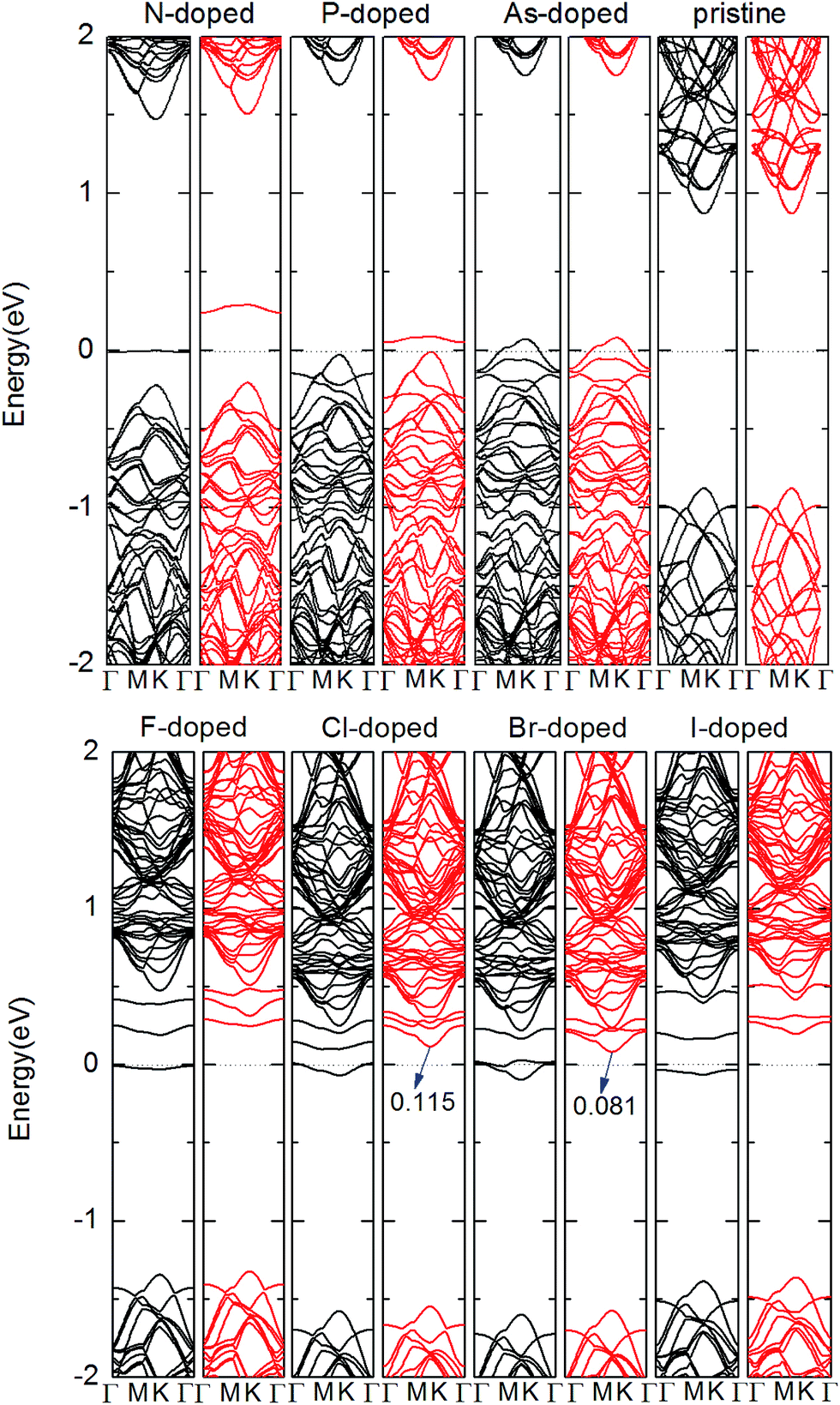 | ||
| Fig. 2 Band structures of pristine and one X-doped 4 × 4 × 1 MoS2 monolayer. The black lines and red lines represent the spin-up and spin-down components, respectively, where the Fermi level is indicated by the dot line. | ||
To gain more insight into the electronic and magnetic properties of the X-doped MoS2 monolayer, the total density of states (TDOS) and partial total density of states (PDOS) of the dopants and neighbor Mo atoms are illustrated in Fig. 3. One can clearly see that the impurity levels of the group V atoms lie close to the valence band maximum (VBM), whereas those of the group VII atoms are close to the conduction band minimum (CBM). This is confirmed from the midgap impurity bands found in the corresponding band structures of Fig. 2. Further, it shows that the impurity bands of the N- and P-doped systems are mostly derived from the Mo dz2 and X pz orbitals near the Fermi level. For the As-doped system, the impurity bands are mostly derived from the Mo dx2 − y2 and As px and py orbitals near the Fermi level. For the group VII atom substitutions, we can see that the impurity bands mainly originate from the hybridization of Mo dxy and dyz, and the F atom pz states near the Fermi level. For the case of the Cl-doped system, the impurity bands mainly originate from the hybridization of Mo dz2 and dx2 − y2, and Cl atom px states near the Fermi level. For the case of the Br- and I-doped systems, the impurity bands mainly come from the hybridization of Mo dz2, and X atom py states near the Fermi level. From Fig. 3, an asymmetrical distribution of DOS can be seen between the majority-spin and minority spin states which produces magnetism in all doped systems. We conclude the magnetic property mainly originates from the doped X atoms and neighboring three Mo atoms. The most important hybridization occurs at 0 eV, where the Fermi level crosses the spin-up states, resulting in the Cl and Br-doped system becoming half-metal. However, for the N, P, F, and I-doped systems, the spin states are not crossed by the Fermi level and distribute asymmetrically, resulting in these systems becoming magnetic nanomaterials. For the case of As-doped, the Fermi level crosses the spin-up and spin-down states and distributes asymmetrically, resulting in As-doped system becoming magnetic metal.
 | ||
| Fig. 3 TDOS and PDOS of X dopants and their neighboring Mo atoms in the X-doped 4 × 4 × 1 MoS2. | ||
Furthermore, the spin density of the X-doped MoS2 monolayer is given in Fig. 4. We can see that a significant portion of the spin density is localized on the X atoms and neighboring three Mo atoms. For the N-, P-, and Br-doped systems, the spin density distribution of dopants and neighboring three Mo atoms is almost symmetrical, which can be attributed to the almost identical bond length of the X atoms and three Mo atoms (see Table 1). But for the F-, and Cl-doped systems, we can see the spin density distribution of the dopants and three Mo atoms is asymmetrical, the hybridization of the X atom and Mo1 and Mo2 is stronger than that of the X atom and Mo3. For the As- and I-doped systems, the hybridization of the X atom and Mo3 is stronger than that of the X atom and Mo1 and Mo2. From Table 1 and Fig. 4, we can see that the p orbital of the N and P atoms plays an important role in the total magnetism in the N- and P-doped systems, but the d orbital of the Mo atoms plays an important role in the total magnetism in As-, F-, Cl-, Br-, I-doped systems.
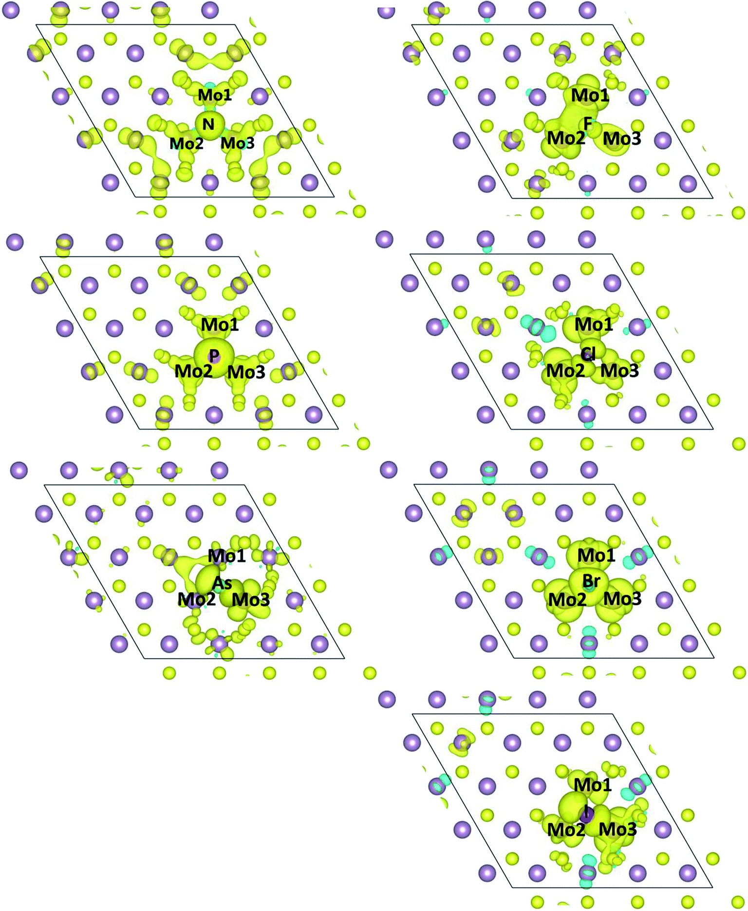 | ||
| Fig. 4 Spin densities of one X dopant and its neighboring Mo atoms in X-doped MoS2. Aqua isosurfaces represent positive spin densities (+0.001 e/Å3). | ||
IV. Conclusion
In summary, we investigated the electronic and magnetic properties of the V- and VII-doped MoS2 monolayer using first-principles methods. We find that group V and VII atoms can induce magnetic properties, and the magnetic moment mainly originates from the dopant’s p orbital and neighboring Mo atoms’ d orbital. N-, P-, F-, and I-doped MoS2 exhibits magnetic nanomaterial features, As-doped MoS2 shows a magnetic metallic feature, the Cl- and Br-doped systems exhibit half-metallic ferromagnetism (HMF) with half-metallic gaps of about 0.115 and 0.081 eV, respectively. Moreover, the formation energy calculations also indicate that it is energetically favorably and relatively easier to incorporate group V and VII atoms into the MoS2 monolayer under Mo-rich experimental conditions. The formation energy of the F-doped system is the lowest of those studied, the next lowest formation energy being obtained in the Cl-doped system. Cl-doped MoS2 is more suitable for spin injection in the future. By comparison, we can see that the p orbital of the N and P atoms plays an important role in the total magnetism of the N- and P-doped systems, but the d orbital of the Mo atoms plays an important role in the total magnetism of the As-, F-, Cl-, Br-, I-doped systems. We believe that these results are helpful for the further study of the properties and applications of MoS2 monolayer based diluted magnetic semiconductors.Acknowledgements
This work is supported by a Grant from the National Natural Science Foundation of China (NSFC) under the Grant No. 11504092, National Undergraduate Training Programs for Innovation and Entrepreneurship (No. 201510476043), Natural science foundation research project of education department of Henan province (No. 2011A140018), Science and technology research key project of education department of Henan province (No. 14A140012), and High Performance Computing Center of Henan Normal University.References
- E. Gourmelon, O. Lignier, H. Hadouda, G. Couturier, J. C. Bernède, J. Tedd, J. Pouzet and J. Salardenne, Sol. Energy Mater. Sol. Cells, 1997, 46, 115 CrossRef CAS.
- P. P. Hankare, A. H. Manikshete, D. J. Sathe, P. A. Chate, A. A. Patil and K. M. Garadkar, J. Alloys Compd., 2009, 479, 657 CrossRef CAS.
- B. Radisavljevic, A. Radenovic, J. Brivio, V. Giacometti and A. Kis, Nat. Nanotechnol., 2011, 6, 147 CrossRef CAS PubMed.
- Q. H. Wang, K. Kalantar-Zadeh, A. Kis, J. N. Coleman and M. S. Strano, Nat. Nanotechnol., 2012, 7, 699 CrossRef CAS PubMed.
- G. Eda, H. Yamaguchi, D. Voiry, T. Fujita, M. W. Chen and M. Chhowalla, Nano Lett., 2011, 11, 5111 CrossRef CAS PubMed.
- M. Thomalla and H. Tributsch, J. Phys. Chem. B, 2006, 110, 12167 CrossRef CAS PubMed.
- T. Drescher, F. Niefind, W. Bensch and W. Grunert, J. Am. Chem. Soc., 2012, 134, 18896 CrossRef CAS PubMed.
- A. M. Seayad and D. M. Antonelli, Adv. Mater., 2004, 16, 765 CrossRef CAS.
- M. Mosleh, N. D. Atnafu, J. H. Belk and O. M. Nobles, Wear, 2009, 267, 1220 CrossRef CAS.
- K. Chang and W. X. Chen, ACS Nano, 2011, 5, 4720 CrossRef CAS PubMed.
- S. A. Wolf, D. D. Awschalom, R. A. Buhrman, J. M. Daughton, S. Von Molnár, M. L. Roukes, A. Y. Chtchelkanova and D. M. Treger, Science, 2001, 294, 1488 CrossRef CAS PubMed.
- D. D. Awschalom and J. M. Kikkawa, Phys. Today, 1999, 52, 33 CrossRef CAS.
- S. A. Wolf, D. D. Awschalom, R. A. Buhrman, J. M. Daughton, S. Von Molnár, M. L. Roukes, A. Y. Chtchelkanova and D. M. Treger, Science, 2001, 294, 1488 CrossRef CAS PubMed.
- D. D. Awschalom and J. M. Kikkawa, Phys. Today, 1999, 52, 33 CrossRef CAS.
- Y. H. Zhao, G. P. Zhao, Y. Liu and B. G. Liu, Phys. Rev. B: Condens. Matter Mater. Phys., 2009, 80, 224417 CrossRef.
- R. A. de Groot, F. M. Mueller, P. G. van Engen and K. H. J. Buschow, Phys. Rev. Lett., 1983, 50, 2024 CrossRef CAS.
- S. J. Luo and K. L. Yao, Phys. Rev. B: Condens. Matter Mater. Phys., 2003, 67, 214429 CrossRef.
- H. M. Huang, S. J. Luo and K. L. Yao, J. Magn. Magn. Mater., 2009, 321, 2200 CrossRef CAS.
- S. M. Watts, S. Wirth, S. von Molnár, A. Barry and J. M. D. Coey, Phys. Rev. B: Condens. Matter Mater. Phys., 2000, 61, 9621 CrossRef CAS.
- P. Mavropoulos and I. Galanakis, J. Phys.: Condens. Matter, 2007, 19, 315221 CrossRef PubMed.
- H. Z. Luo, Z. Y. Zhu, G. D. Liu, S. F. Xu, G. H. Wu, H. Y. Liu, J. P. Qu and Y. X. Li, J. Magn. Magn. Mater., 2008, 320, 421 CrossRef CAS.
- H. Rached, D. Rached, R. Khenata, A. H. Reshak and M. Rabah, Phys. Status Solidi B, 2009, 246, 1580 CrossRef CAS.
- I. Galanakis and Ph. Mavropoulos, Phys. Rev. B: Condens.Matter Mater. Phys., 2003, 67, 104417 CrossRef.
- Y. Xing, Y. Liu, S. N. Li, Y. H. Zhao and W. H. Xie, Phys. Status Solidi B, 2010, 247, 2268 CrossRef CAS.
- H. Ohno, A. Shen, F. Matsukura, A. Oiwa, A. Endo, S. Katsumoto and Y. Iye, Appl. Phys. Lett., 1996, 69, 363 CrossRef CAS.
- T. Dietl, Nat. Mater., 2010, 9, 965 CrossRef CAS PubMed.
- C. Ataca and S. Ciraci, J. Phys. Chem. C, 2011, 115, 13303 CAS.
- Y. Zhou, P. Yang, H. Zu, F. Gao and X. Zu, Nanoholes Nanodots and Antidots, Phys. Chem. Chem. Phys., 2013, 15, 10385–10394 RSC.
- S. W. Han, Y. H. Hwang, S.-H. Kim, W. S. Yun, J. D. Lee, M. G. Park, S. Ryu, J. S. Park, D. H. Yoo and S.-P. Yoon, et al., Phys. Rev. Lett., 2013, 110, 247201 CrossRef PubMed.
- Y. Ma, Y. Dai, M. Guo, C. Niu, J. Lu and B. Huang, Phys. Chem. Chem. Phys., 2011, 13, 15546–15553 RSC.
- S. Tongay, S. S. Varnoosfaderani, B. R. Appleton, J. Wu and A. F. Hebardet, Appl. Phys. Lett., 2012, 101, 123105 CrossRef.
- L. Kou, C. Tang, Y. Zhang, T. Heine, C. Chen and T. Frauenheim, J. Phys. Chem. Lett., 2012, 3, 2934–2941 CrossRef CAS PubMed.
- P. Lu, X. Wu, W. Guo and X. C. Zeng, Phys. Chem. Chem. Phys., 2012, 14, 13035–13040 RSC.
- E. Durgun, D. I. Bilc, S. Ciraci and P. Ghosez, J. Phys. Chem. C, 2012, 116, 15713 CAS.
- Y. Xie and J. M. Zhang, Comput. Theor. Chem., 2011, 976, 215 CrossRef CAS.
- Y. C. Cheng, Z. Y. Zhu, W. B. Mi, Z. B. Guo and U. Schwingenschlögl, Phys. Rev. B: Condens. Matter Mater. Phys., 2013, 87, 100401(R) CrossRef.
- A. Ramasubramaniam and D. Naveh, Phys. Rev. B: Condens. Matter Mater. Phys., 2013, 87, 195201 CrossRef.
- R. H. Mishra, W. Zhou, S. J. Pennycook, S. T. Pantelides and J. C. Idrobo, Phys. Rev. B: Condens. Matter Mater. Phys., 2013, 88, 144409 CrossRef.
- H. Ohno, A. Shen, F. Matsukura, A. Oiwa, A. Endo, S. Katsumoto and Y. Iye, Appl. Phys. Lett., 1996, 69, 363 CrossRef CAS.
- K. Sato, L. Bergqvist, J. Kudrnovský, P. H. Dederichs, O. Eriksson, I. Turek, B. Sanyal, G. Bouzerar, H. Katayama-Yoshida, V. A. Dinh, T. Fukushima, H. Kizaki and R. Zeller, Rev. Mod. Phys., 2010, 82, 1633 CrossRef CAS.
- H. Ohno, Science, 1998, 281, 951 CrossRef CAS PubMed.
- X. Zhao, C. X. Xia, T. X. Wang and X. Q. Dai, Solid State Commun., 2015, 220, 31–35 CrossRef CAS.
- X. Zhao, C. X. Xia, T. X. Wang and X. Q. Dai, J. Alloys Compd., 2016, 654, 574–579 CrossRef CAS.
- C. W. Zhang and S. S. Yan, Appl. Phys. Lett., 2009, 95, 232108 CrossRef.
- S. W. Fan, K. L. Yao, Z. L. Liu, G. Y. Gao, Y. Min and H. G. Cheng, J. Appl. Phys., 2008, 104, 043912 CrossRef.
- H. Pan, Y. P. Feng, Q. Y. Wu, Z. G. Huang and J. Y. Lin, Phys. Rev. B: Condens. Matter Mater. Phys., 2008, 77, 125211 CrossRef.
- S. S. Li, C. W. Zhang, F. Li, W. X. Ji, P. Li, M. J. Ren, P. J. Wang and M. Yuan, RSC Adv., 2014, 4, 24399–24405 RSC.
- C. W. Zhang and S. S. Yan, Appl. Phys. Lett., 2009, 95, 232108 CrossRef.
- F. B. Zheng, C. W. Zhang, S. S. Yan and F. Li, J. Nanopart. Res., 2013, 15, 1647 CrossRef.
- Y. F. Chen, Q. G. Song, H. Y. Yan, X. Yang and T. Wei, Solid State Commun., 2011, 151, 619–623 CrossRef CAS.
- K. F. Mak, C. Lee, J. Hone, J. Shan and T. F. Heinz, Phys. Rev. Lett., 2010, 105, 136805 CrossRef PubMed.
- A. Splendiani, L. Sun, Y. Zhang, T. Li, J. Kim, C. Y. Chim, G. Galli and F. Wang, Nano Lett., 2010, 10, 1271–1275 CrossRef CAS PubMed.
- Y. H. Lee, X. Q. Zhang, W. Zhang, M. T. Chang, C. T. Lin, K. D. Chang, Y. C. Yu, J. T. W. Wang, C.-S. Chang and L. J. Li, et al., Adv. Mater., 2012, 24, 2320–2325 CrossRef CAS PubMed.
- W. Zhou, X. Zou, S. Najmaei, Z. Liu, Y. Shi, J. Kong, J. Lou, P. M. Ajayan, B. I. Yakobson and J.-C. Idrobo, Nano Lett., 2013, 13, 2615–2622 CrossRef CAS PubMed.
- P. E. Blochl, Phys. Rev. B: Condens. Matter Mater. Phys., 1994, 50, 17953 CrossRef.
- G. Kresse and J. Furthmüller, Phys. Rev. B: Condens. Matter Mater. Phys., 1996, 54, 11169 CrossRef CAS.
- J. P. Perdew, K. Burke and M. Ernzerhof, Phys. Rev. Lett., 1996, 77, 3865 CrossRef CAS PubMed.
- C. X. Xia, Y. T Peng, S. Y. Wei and Y. Jia, Acta Mater., 2013, 61, 7720–7725 CrossRef CAS.
- C. X. Xia, Y. T Peng, H. Zhang, T. X. Wang, S. Y. Wei and Y. Jia, Phys. Chem. Chem. Phys., 2014, 16, 19674 RSC.
- Y. T Peng, C. X. Xia, H. Zhang, T. X. Wang, S. Y. Wei and Y. Jia, Phys. Chem. Chem. Phys., 2014, 16, 18799 RSC.
- Y. T Peng, C. X. Xia, H. Zhang, T. X. Wang, S. Y. Wei and Y. Jia, J. Appl. Phys., 2014, 116, 044306 CrossRef.
- C. X. Xia, Y. Jia, M. Tao and Q. Zhang, Phys. Lett. A, 2013, 377, 1943 CrossRef CAS.
- X. Zhao, C. X. Xia, T. X. Wang, Y. T. Peng and X. Q. Dai, J. Alloys Compd., 2015, 649, 357–361 CrossRef CAS.
| This journal is © The Royal Society of Chemistry 2016 |