
 Open Access Article
 This Open Access Article is licensed under a Creative Commons Attribution-Non Commercial 3.0 Unported Licence
Flexible and transparent electrodes imprinted from Au nanowires: stability and ageing†
Lukas F.
Engel
 a,
Lola
González-García
*a and
Tobias
Kraus
*ab
a,
Lola
González-García
*a and
Tobias
Kraus
*ab
aINM – Leibniz Institute for New Materials, Campus D2 2, 66123 Saarbrücken, Germany. E-mail: tobias.kraus@leibniz-inm.de; lola.gonzalez-garcia@leibniz-inm.de; Tel: +49 (0)681-9300-269, +49 (0)681-9300-389
bColloid and Interface Chemistry, Saarland University, Campus D2 2, 66123 Saarbrücken, Germany
First published on 29th July 2022
Abstract
We study the stability of flexible transparent electrodes (FTEs) that were self-assembled from ultra-thin gold nanowires (AuNW) by direct nanoimprinting of inks with different particle concentrations (1 to 10 mg mL−1). The resulting lines were less than 3 μm wide and contained bundles of AuNW with oleylamine (OAm) ligand shells. Small-angle X-ray scattering confirmed a concentration-independent bundle structure. Plasma sintering converted the wire assemblies into lines with a thin metal shell that contributes most to electrical conductivity and covers a hybrid core. We studied the relative change in sheet resistance and the morphology of the FTEs with time. The sheet resistance increased at all concentrations, but at different rates. The metal shell aged by de-wetting and pore formation. The hybrid core de-mixed and densified, which led to a partial collapse of the shell. Residual organics migrated through the shell via its pores. Lines formed at low concentration (cAu = 2 to 3 mg mL−1) contained less residual organics and aged slower than those formed at high cAu ≥ 5 mg mL−1. We passivated the conductive shell with thin, adsorbed layers of PEDOT:PSS and found that it decelerated degradation by slowing surface diffusion and hindering further rupture of the shell. Thick capping layers prevented degradation entirely and stopped pore formation.
1 Introduction
Ultra-thin gold nanowires (AuNW) have core diameters dw ≈ 1.7 nm,1 a shell of oleylamine (OAm), and lengths around lw ≈ 3 to 6 μm.2,3 They are suitable as building blocks of flexible and transparent electrodes (FTEs).4,5 The wires form in a simple one-pot synthesis,6 and have a conductive7 and chemically inert8 Au core and a low percolation threshold9 due to their high aspect ratio lw![[thin space (1/6-em)]](https://www.rsc.org/images/entities/char_2009.gif) :dw > 103. Purification and re-dispersion of the AuNW in cyclohexane provides colloidal inks of varying Au concentration cAu (AuNW inks) in which >70% of the wires self-assemble into bundles even at low cAu = 1 mg mL−1.10 Maurer et al.5 showed that direct nanoimprinting of AuNW inks leads to the self-assembly of AuNW bundles on flexible, transparent polyethylene terephthalate (PET) foils.
:dw > 103. Purification and re-dispersion of the AuNW in cyclohexane provides colloidal inks of varying Au concentration cAu (AuNW inks) in which >70% of the wires self-assemble into bundles even at low cAu = 1 mg mL−1.10 Maurer et al.5 showed that direct nanoimprinting of AuNW inks leads to the self-assembly of AuNW bundles on flexible, transparent polyethylene terephthalate (PET) foils.
Transparent electrodes are key components11 in opto-electronic devices12 to collect charges from layers, e.g. in solar cells, or to supply layers with charge carriers, e.g. in light-emitting diode displays.13 Transparent electrodes for light and flexible devices14 should provide low sheet resistance, high optical transmittance, good mechanical flexibility, and long term stability. Thin metal grids have the potential to combine these characteristics.
Grids with arbitrary geometry and sub-micron line width are attainable under ambient conditions in an efficient roll-to-roll compatible process using a soft silicone elastomer stamp as described by Maurer et al.5 The ink is confined in the stamp's cavities and the solvent (cyclohexane) permeates through the silicone. Ligand-dominated supra-molecular interactions cause the wires to bundle into hierarchical, percolating superstructures in the stamp's features. A soft plasma sintering step in a 5% H2 in Ar (H2/Ar) atmosphere removes insulating OAm ligands while retaining the overall imprinted structure and turns the grid into a conductive electrode. Maurer et al.5 nanoimprinted FTEs with square, hexagonal, and line-like features on PET and found optical transmittances ≥90% over the entire visible range and sheet resistances Rsh ranging from 106 to 168 Ωsq with better mechanical flexibility than commercial electrodes based on tin-doped indium oxide (ITO).
In our previous work,15 we studied the effect of the grid line morphology of AuNW-derived FTEs on their opto-electronic performance as a function of gold concentration cAu and found that plasma sintering removed the insulating OAm ligands only partially. The plasma-sintered lines have thin conductive Au shells covering an insulating hybrid core. The thickness tshell of the porous shell is virtually independent of cAu (tshell = 5.66 ± 1.06 nm). Thin, porous metal films are prone to de-wetting,16 and AuNW are prone to the Rayleigh–Plateau instability,17–19 which raises the question of stability for electrodes imprinted from AuNWs.
The stability of random silver nanowire (AgNW) network electrodes has been studied extensively.13,20–25 They were found to be sensitive to UV light, chemical corrosion by sulfides, oxygen, and acids; the wires undergo thermally activated spheroidization due to the Rayleigh–Plateau instability and can fail through electromigration. Stability was improved by coatings that protect the metal surface from corrosion or reduce its diffusivity.
Few studies exist on the stability of AuNW based electrodes. Maurer et al.26 prepared ≈10 nm thick, disordered layers of AuNW on glass via dip-coating at cAu ≈ 2 mg mL−1, subjected them to plasma sintering in O2 or H2/Ar for different periods, and investigated their stability under ambient conditions. Untreated AuNW layers were non-conductive and fragmented within one week. Plasma sintering for 1 min led to conductive layers whose Rsh exceeded the measurable range after 4 h. The AuNW fragmented into spheres with diameters above those expected for the Rayleigh–Plateau instability, suggesting subsequent Ostwald ripening. Plasma sintering for 5 min or 15 min led to conductive layers that were stable for at least 4 months. Maurer et al.26 concluded that OAm slows wire fragmentation, whereas partial OAm removal accelerates it.
In a different study, Maurer et al.27 prepared ≈3 nm and ≈9 nm thick disordered AuNW layers on glass by dip-coating at cAu ≈ 3 mg mL−1 and investigated their stability at 120 °C, 180 °C, and 250 °C with and without plasma sintering in H2/Ar. Unsintered AuNW fragmented within 30 min of annealing, followed by a ripening process. Annealing of sintered layers caused de-wetting that accelerated with increasing temperature and decreasing film thickness. We are not aware of any studies on the stability of structured AuNW layers.
Here, we report on the stability of grid-like FTEs imprinted from AuNW. Arrays of about 1.6 μm wide, parallel lines with a pitch of 19.5 μm and heights of up to ≈275 nm were imprinted with inks of different cAu on PET foils as in Engel et al.,15 analyzed with small-angle X-ray scattering (SAXS), and sintered in H2/Ar plasma. Their Rsh was monitored during storage under ambient conditions in the dark and correlated with the grid morphology from scanning (SEM) and transmission electron microscopy (TEM). The sheet resistance Rsh increased at all cAu, but the rates depended on cAu and the line height. The decisive factor was the fraction of residual organics in the partially sintered cores. We adsorbed thin layers of PEDOT:PSS and found that it slowed electrode degradation. A thick capping layer of PEDOT:PSS prevented degradation and resulted in a slow decrease of Rsh during ≈3.5 months.
2 Materials and methods
2.1 Synthesis of Au nanowires
For a typical synthesis, 60 mg of HAuCl4·3H2O (10 mM) were placed in a disposable 50 mL glass snap-on vial from Carl Roth GmbH + Co. KG (Karlsruhe, Germany), followed by 9.9 mL of n-hexane and 2.04 mL of oleylamine (400 mM). The resulting mixture was vortexed for 1 min to obtain a solution. To the solution, 3.06 mL (1 M) of triisopropylsilane (TIPS) were added as reducing agent. The mixture was vortexed for 30 s and then left to itself in an oven at 25 °C for 24 h.
The weighing of the very hygroscopic HAuCl4·3H2O was carried out in a glove box from SylaTech GmbH (Walzbachtal, Germany) since the presence of water causes shorter wires.29 The glass snap-on vial was pre-flushed with dry Ar. OAm and TIPS were added with a 5 mL pipette in the given order and immediate succession.
2.2 Nanoimprinting
Silanization of the silicon master was directly performed, while silanization of the PDMS master was performed after its plasma activation for 1.5 min using an oxygen plasma at 0.3 mbar in a low pressure plasma reactor of type Pico from Diener electronic GmbH & Co. KG (Ebhausen, Germany). Silanization of each master was performed by vapour phase deposition inside a conventional glass desiccator with a snap-on vial cap containing 30 μL of (tridecafluoro-1,1,2,2-tetrahydrooctyl)trichlorosilane from abcr GmbH (Karlsruhe, Germany). The snap-on vial cap was shielded from the masters to achieve uniform silanization. The desiccator was flushed with Ar, evacuated to 3 mbar, and disconnected from the vacuum pump. After 30 min, the desiccator was slowly ventilated with air.
The pre-polymer and the cross-linker of a PDMS kit, Sylgard 184 from Dow Inc. (Midland, USA), were mixed in a 10:1 (w/w) ratio and degassed in a Speedmixer DAC 600.2 VAC-P from Hauschild GmbH & Co. KG (Hamm, Germany) at a speed of 2350 rpm and a pressure of 1 mbar for 3 min so that no air bubbles remained. This mixture was poured onto the respective master. A Teflon ring (2 mm thick) which was sealed at the edges with add-i-gum light N from DE Healthcare Products (Gillingham, UK) and on top with a glass plate, was used as a spacer to ensure uniform thickness. Before carefully peeling off the replicate along the stamp channels, the PDMS was cured at 80 °C for 3 h.
The replicates of the PDMS masters were cut into two halves, each constituting an imprinting stamp. Both had an area of 3.5 cm × 8 cm of which 3.5 cm × 7 cm were patterned and 3.5 cm × 0.5 cm at either end were not. The latter were run-in and run-out areas during imprinting.
2.3 Plasma sintering
Plasma sintering was performed in a low pressure 13.56 MHz RF plasma reactor of type Pico from Diener electronic GmbH & Co. KG (Ebhausen, Germany) right after imprinting. A mixture of 5% H2 in Ar was used as process gas. The sintering conditions were: room temperature and ≈0.3 mbar for 20 min with 100 W RF power.2.4 Small-Angle X-Ray Scattering (SAXS)
The structural arrangement of the wires within the pre-plasma lines was studied in transmission via SAXS on PET right after imprinting. Any influence of applied vacuum was avoided by performing the measurements in air at room temperature. Background scattering due to the substrate was measured separately as reference. The scattering instrument was a Xeuss 2.0 HR SAXS/WAXS instrument from Xenocs SAS (Grenoble, France) with a Cu Kα source. The detector was a PILATUS3 R 1 M from DECTRIS AG (Baden, Switzerland) which was set up at a distance of ≈550 mm from the samples. The distance was precisely calibrated with a Ag behenate sample prior to each measurement. Samples were measured for a total of 2 h each. The 2D scattering images were azimuthally integrated over an angular sector at 90° and an aperture angle of 10° (to take the anisotropy due to the alignment of wires in imprinting direction into account) with the software Foxtrot from Synchrotron SOLEIL (Saint-Aubin, France) to obtain the scattering curves.2.5 Sheet resistance measurements
Electrical resistances were measured in 2-point-probe configuration using a multi-channel multi-meter (DAQ6510 data acquisition logging multi-meter system) equipped with multiplexer cards (7702 40-channel differential multiplexer module with screw terminals) from Keithley Instruments GmbH (Germering, Germany). Electrodes were contacted by applying a fast drying Ag paste ACHESON Ag DAG 1415 from Plano GmbH (Wetzlar, Germany) and AGF 1 miniature crocodile clamps from SKS Kontakttechnik GmbH (Niederdorf, Germany). The Ag paste was deposited in two parallel lines, each 1.5 cm long and spaced 1.5 cm apart, yielding a square measurement field. This caused the measured resistances being equal to the desired sheet resistances. Measurements were automatically recorded every 10 min during storage under controlled ambient conditions (T ≈ 22 °C, rH ≈ 55%) in the dark. Light was excluded to avoid e.g. radiation heating.2.6 Dip coating
Electrodes were dip coated in an aqueous PEDOT:PSS dispersion of type Clevios™ P from Heraeus Deutschland GmbH & Co. KG (Hanau, Germany) right after plasma treatment (taking advantage of the plasma's hydrophilising effect) and the subsequent preparation for contacting. For contacting purposes, a fast drying Ag paste ACHESON Ag DAG 1415 from Plano GmbH (Wetzlar, Germany) was applied as described in the section above. The contacted electrodes were slowly dipped into the dispersion and were then immediately pulled out again slowly. Excess PEDOT:PSS was either allowed to drip off (capping layer) or was washed off (adsorbate layer) in deionised water by carefully moving the electrode up and down until no more PEDOT:PSS residues were visible (PEDOT:PSS is deep blue) and presumably only a thin layer of chemisorbed PEDOT:PSS remained (Au–S bond). Such coated electrodes were then dried for 15 min in a drying oven at 50 mbar and room temperature. Afterwards, for the electrodes from which the excess PEDOT:PSS only dripped off, the Ag paste contacting was gently freed from the PEDOT:PSS capping layer using mini head clean room polyester swabs moistened with deionised water.2.7 Cross-sectioning via Focused Ion Beam (FIB)
Cross-sections of printed and of sintered lines were prepared using a FEI Versa 3D DualBeam from Thermo Fisher Scientific GmbH (Schwerte, Germany). The surfaces of the lines were protected by Pt-layers first deposited by an electron beam, then with an ion beam.2.8 Transmission Electron Microscopy (TEM)
All TEM lamellae from FIB cross-sectioning were imaged at an acceleration voltage of 200 kV in a JEM 2010 from JEOL GmbH (Freising, Germany).2.9 Scanning Electron Microscopy (SEM)
Scanning electron micrographs were taken with a FEI Quanta 400 ESEM or a FEI Versa 3D DualBeam from Thermo Fisher Scientific GmbH (Schwerte, Germany) using the secondary electron detectors. For better imaging, the grids were imprinted onto polished, p-type Si wafers from Siegert Wafer GmbH (Aachen, Germany).3 Results and discussion
We prepared inks from oleylamine-covered gold nanowires and printed grids at different nanowire concentrations on flexible polyethylene terephthalate (PET) foils using the same stamp. All grids underwent plasma sintering to obtain electrically conductive FTEs. We monitored the change in their sheet resistance Rsh over a storage period of 14 days at a constant temperature T ≈ 22 °C and a humidity of rH ≈ 55% in the dark. Fig. 1 shows the change in Rsh as a function of the ink concentration. The lowest concentration of cAu = 2 mg mL−1 was the minimum to achieve sufficient percolation and reasonable conductivities. The highest cAu = 6 mg mL−1 marks the concentration from which on ageing became concentration-independent.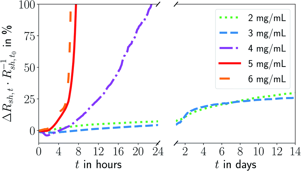 | ||
| Fig. 1 Relative change in sheet resistance (Rsh,t − Rsh,t0)Rsh,t0−1 = ΔRsh,tR−1sh,t0 after time t for electrodes imprinted at different ink concentrations cAu. The results of repeated experiments and additional concentrations are shown in Fig. S1 in the ESI.† | ||
The sheet resistances of all electrodes increased with time. The rate of increase was much larger for electrodes imprinted at 5 mg mL−1 than at 3 mg mL−1. The resistance of electrodes imprinted at 3 mg mL−1 increased by ≈30% within 14 days of ageing; electrodes imprinted at 5 mg mL−1 became non-conductive within 8 h.
Fig. 2 and 3 show electron micrographs of the surfaces and cross-sections of relatively stable grid lines imprinted at 2 mg mL−1 (“low cAu”) and highly unstable lines imprinted at 6 mg mL−1 (“high cAu”), respectively. Images were taken directly after imprinting, after plasma sintering, and after 24 h of storage under ambient conditions (T ≈ 22 °C, rH ≈ 55%) in the dark. Plasma sintering led to a structure with a thin shell, a coarsened core, and a loss in height (compare panel A with C and B with D). Height loss continued during ageing with the core further densifying (compare panel C with E and D with F). At high cAu, ageing also caused de-mixing inside the core (Fig. 3F) and rupture of the shell (Fig. 3E). This is consistent with the illustrations in panels G–I, which illustrate the associated change in the line structure: orange depicts gold wires or shells, with the wires arranged in hexagonal bundles (dotted black lines); green indicates oleylamine ligand molecules and their fragments (residual organics).
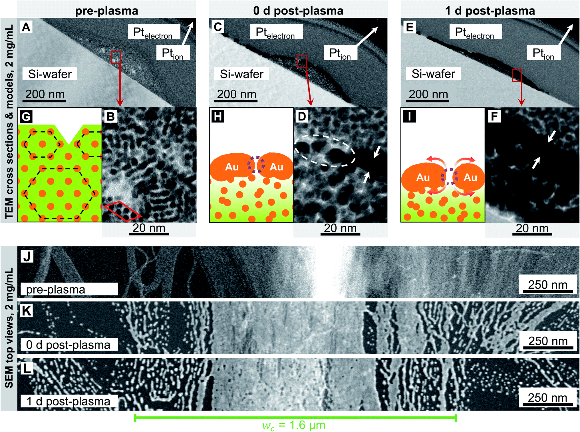 | ||
| Fig. 2 Cross-sections and surfaces of lines imprinted at 2 mg mL−1 before (A, B and J), immediately after (C, D and K), and one day after (E, F and L) plasma sintering. They show the core–shell structure after plasma sintering (C and D), the densifying (A, C and E) and coarsening (B, D and F) core, and the coarse surface morphology with small pores in the shell (from K to L). The illustrations in panels (G–I) illustrate the overall structure. Orange depicts gold wires or shells, green indicates oleylamine ligand molecules and their fragments (residual organics). The wires are arranged in hexagonal bundles (dotted black lines) in (G). They form porous shells in (H), and the bundles loose their order. The pores in (I) have gently grown by surface diffusion and the densifying core causing the shell to collapse. | ||
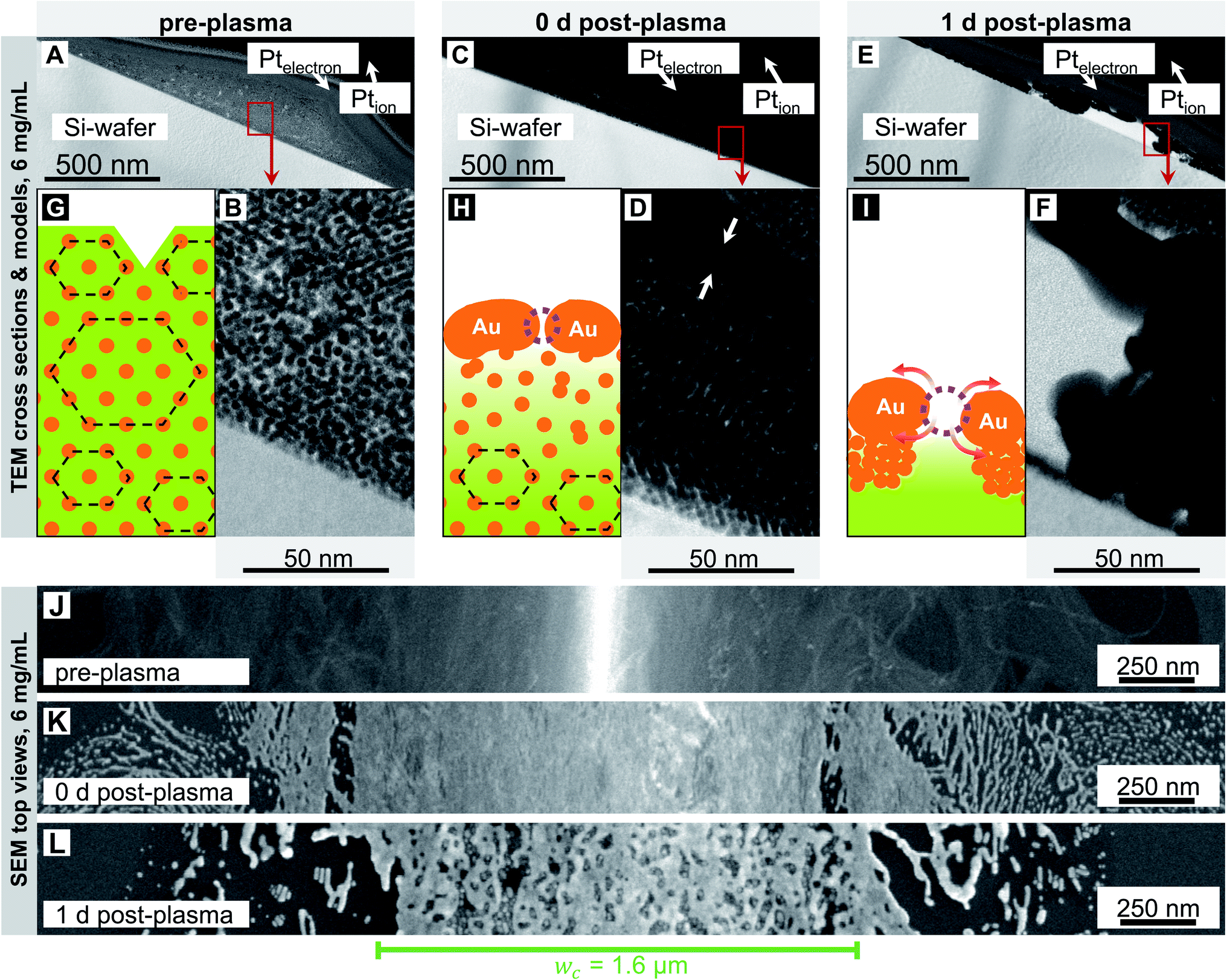 | ||
| Fig. 3 Cross-sections and surfaces of lines imprinted at 6 mg mL−1 before (A, B and J), immediately after (C, D and K), and one day after (E, F and L) plasma sintering. They show the core–shell structure after plasma sintering (C and E), the densifying (A, C and E) and coarsening (B, D and F) core, and the coarse surface morphology with growing pores (from K to L). The illustrations in panels (G–I) illustrate the overall structure. Orange depicts gold wires or shells, green indicates oleylamine ligand molecules and fragments. The wires are arranged in hexagonal bundles (dotted black lines) in (G). They form porous shells in (H), and the bundles loose their order. The pores in (I) have grown prominently by surface diffusion and by the both de-mixing and densifying core causing the shell to collapse. | ||
We first consider lines printed at low cAu in more detail (Fig. 2). The pre-plasma lines (Fig. 2A) contained AuNW in hexagonally packed bundles. They are visible in the TEM cross-section in Fig. 2B and caused peaks in SAXS (Fig. S2 in the ESI†). The bundle packing was noticeably denser than inside the ink, with a center-to-center distance ac–c = 4.22 ± 0.04 nm versus ainkc–c = 5.9 ± 0.02 nm in liquid.10 The surface-to-surface distance of the gold cores was as–s ≈ 2.52 nm. as–s is only ≈23% above the length of an OAm molecule (lOAm ≈ 2.05 nm (ref. 32)), probably due to a zipper-like interdigitation of the OAm shells.31
Most of the wires were well aligned in lines that were narrower than the channel width of the imprinting stamp. Some wires bleeded beyond the channel width; these were only partially aligned in imprinting direction (Fig. 2J). The surface of the freshly printed lines exhibited a ridge that is visible as a bright area in Fig. 2J. Fig. 2G shows an illustration of the rough surface of the lines before plasma sintering that is caused by the bundled wires.
Plasma sintering formed a thin metal shell around a hybrid core (Fig. 2C and D). The surface of the sintered line appears coarse, the ridge is blunted (Fig. 2K), and the wire bundle structure is lost (Fig. 2D). The shell was porous and has holes indicated in Fig. 2D. Shell porosity likely results from the bundle-induced roughness. Wires may partially fragment before they sinter.18 Thin layers of sparse AuNW adjacent to the main line fragmented, probably due to the Rayleigh–Plateau instability.17–19 They formed finger-like structures that indicate solid-state de-wetting.16
The morphology of the core (Fig. 2B) visibly coarsened during sintering (Fig. 2D) through its entire thickness (Fig. S3 in the ESI†) of up to hmax = 68 ± 14 nm.15 A relevant fraction of OAm has apparently been removed. This likely turns the core partially porous, too. The initial OAm content was ≈87 vol%10 (see Section 2.2 in the ESI†). The plasma's kinetic ions remove the ligands and enhance the Au surface mobility,33–37 which renders the wires highly susceptible to the Rayleigh–Plateau instability.26 There probably exists a gradient in the residual organic concentration from the shell (Fig. 2H, very light green) towards the substrate (Fig. 2H, darker green), as the plasma sintering attacks from the outside.38
We stored the samples for 24 h and analyzed morphological changes. The core appeared denser (Fig. 2C–F), probably because the cores' pores began to close, and the maximum line height hmax decreased (compare Fig. 2C and E). Small pores appeared on the surface. They are clearly visible in the SEM top view (Fig. 2L) but not in the cross-sectional TEM (Fig. 2E and F) that show lamellae with a thickness on the order of ≈200 nm. The pores probably form by solid-state de-wetting and the shrinkage of the core that compensates for the loss of OAm. Solid-state de-wetting starts at pre-existing holes (visible in Fig. 2D) in the thin shell. De-wetting requires diffusion and is faster for decreasing shell thicknesses.16 A continuous, ≈6 nm thick Au film does not de-wet at room temperature during 24 h.16 It is thus likely that the compacting core is more important for the ageing of the line. This is consistent with the unchanged microstructures on both sides of the printed lines (Fig. 2LversusFig. 2K) that did not de-wet. The increase in shell porosity increased Rsh by only 7.3% within 24 h. Apparently, the pores were small in size, and relaxation effects after plasma sintering that release stress and lattice distortions39 in the shell counteracted a larger increase in Rsh. Compared with Fig. 2H and I shows an illustration with a slightly thicker shell, an increased pore size and due to the shrinking core a lower height. As the core has densified, the residual organics are now distributed within a smaller volume (represented by a slightly darker shade of green in Fig. 2I).
We now consider the lines printed at high particle concentration in more detail (Fig. 3). Before plasma-sintering, SAXS confirmed the same 2D hexagonal arrangement of the AuNW as observed at low concentrations (Fig. S2 in the ESI†). The morphology seen in TEM cross-sections appears unchanged, too (Fig. 3A and B). SEM top-views show wider lines with w > wc (Fig. 3J), but the surface morphology appears similar to that seen at 2 mg mL−1 (Fig. 2J). The most relevant change in line morphology before plasma sintering seems to be the increased height (compare Fig. 3A and 2A).
Plasma sintering yielded the same core–shell structure as described above. The pores in the shell are not visible in the TEM images (Fig. 3C and D) but have been identified in our previous work.15 A pronounced gradient in core density that decreased towards the substrate was visible in the cross-sections (compare Fig. 3B with D). We did not observe such strong gradients at lower concentrations, probably because those lines were thinner. The gradient likely results from partial removal of OAm that is more efficient close to the shell. The overall morphology of the sintered lines did not change with ink concentration and remained as shown in Fig. 2H, but with adjusted height and structural gradient (Fig. 3H).
Ageing for 24 h caused the shell to become increasingly porous (Fig. 3E). The density of pores was similar to that at 2 mg mL−1, but the pores were larger (compare top view SEM images in Fig. 3LversusFig. 2L). Some of the pores joined into large cracks that revealed the fragmented wires of the core. The hybrid core appeared heterogeneously densified and de-mixed (Fig. 3E and F); metallic gold accumulated on the fragmented shell. The metal-rich volumes appear to contain larger spheres, possibly formed by wires undergoing Rayleigh–Plateau fragmentation,17–19 and possibly growing by Ostwald ripening.40Fig. 3I shows an illustration of the de-mixing core–shell structure.
These results suggest that the same mechanisms are responsible for the ageing of sintered lines printed at 2 mg mL−1 and 6 mg mL−1, but that they operate at larger rates for the higher concentration. The reason likely is the increased fraction of residual organic molecules in the cores of sintered lines printed at high concentration. Inks with high cAu form thicker lines that are not fully penetrated by the plasma and thus remain richer in OAm and its fragments. The low binding energy of Au–NH2,41,42 the partial fragmentation of OAm, and the low viscosity8 of OAm at room temperature increase the mobility of the core components43–45 and accelerate ageing. This effect apparently saturates at high fractions of residual organics reached at 6 mg mL−1.
We conclude that some of the advantages that AuNWs have for the nanoimprinting of conductive structures limit the stability of the resulting structures. The wires' mechanical flexibility and high aspect ratio promote percolation but lead to coarse surface microstructures of the unsintered lines (see Fig. 2J and 3J), causing pores in the conductive shell which foster solid-state de-wetting after plasma sintering. The wires' small diameters make them susceptible to the Rayleigh–Plateau instability,17–19 which renders only partially sintered line cores unstable; the weakly bound OAm shell41,42 that occupies approximately ≈87 vol%10 of the pre-plasma solid turns the sintered parts of the line core porous, and its residues accelerate de-mixing.43–45
Lines printed at low ink concentrations are comparatively thin, and the OAm is largely removed from them during plasma sintering. This slows solid-state de-wetting of the shell and makes the electrodes comparatively stable. Lines printed at high concentrations are thicker, remain rich in OAm and its fragments after sintering. They age faster so that electrodes fail in less than 24 h. The transition from comparatively stable to highly unstable electrodes coincides with the concentration at which the line width w reaches the channel width wc of the imprinting stamp (4 mg mL−1). Above this concentration, the maximum line height hmax increases faster than the line width.15
How can we stabilize AuNW electrodes? Full sintering of the printed lines would reduce mobility and thus obviate several ageing mechanisms identified above. Plasma sintering of AuNW grids is self-limiting,38 however, and excludes full sintering of the thick lines imprinted at high cAu that have the best performance.15 The shell shields the core from the plasma and contains the (partially fragmented) OAm. We are not aware of any other existing sintering technique that could retain the structure of the printed lines but remove all organic content.
An alternative approach is to stabilize the conductive shell. Metal thin films can be stabilized using adsorbates that prevent or slow the diffusive processes underlying solid-state de-wetting.16 A promising material for that purpose is PEDOT:PSS, a mixture of the positively charged poly(3,4-ethylenedioxythiophene) and the negatively charged polystyrene sulfonate. There is evidence that polythiophenes bind covalently to Au via sulphur.46,47 Their molecular configuration depends on the crystallographic orientation and the curvature of the Au surface.48
We used the commercial PEDOT:PSS aqueous dispersion Clevios™ P that contains swollen, gel-like PEDOT:PSS particles of diameter d50 = 80 nm at a PEDOT:PSS weight ratio of 1:2.5 and a pH of 1.9 without any additives.49,50 While its acidity is harmful for AgNWs,24 it does not etch AuNWs. Dried films of Clevios™ P exhibit conductivities of 5 S cm−1,50 five orders of magnitude below that of the Au shells.15 We used dip-coating to prepare electrodes with adsorbate layers of PEDOT:PSS. Excess PEDOT:PSS was removed by washing in water to retain only the adsorbed film; some samples were not washed to retain a thicker capping layer after drying. Note that rough and porous Au surfaces improve the bonding of PEDOT:PSS.51 The samples were then stored under ambient conditions (T ≈ 22 °C, rH ≈ 55%) in the dark and we analyzed their ageing.
Fig. 4 shows the relative change in sheet resistance of electrodes imprinted at 6 mg mL−1 for different coatings (A–C) and the reconstructed morphology illustrations (D–F). Bare electrodes deteriorated fast (five-fold increase of Rsh in roughly 7 h) and became insulating in less than 1 day. Their relative change in Rsh increased exponentially (Fig. 4A). The resistance of electrodes with a PEDOT:PSS adsorbate layer initially decreased by up to ≈16% and then slowly increased with an almost linear trend, so that Rsh quintupled after 62 days (Fig. 4B). It is likely that the adsorbed PEDOT:PSS layer prevents a fast rupture of the shell but cannot entirely suppress diffusion at the shell's Au–air and neither at the core's Au–OAm residue interfaces. It cannot fully stabilize the shell mechanically when the hybrid core shrinks.
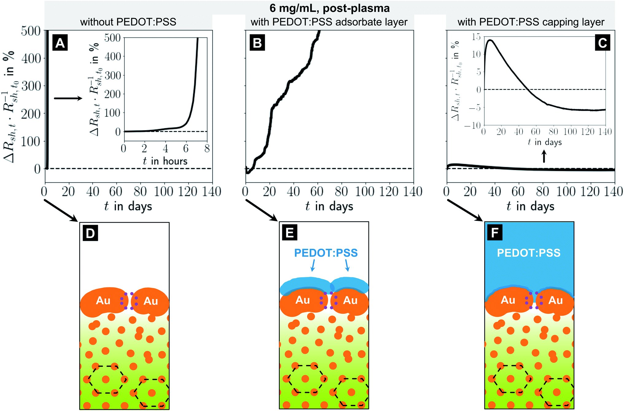 | ||
| Fig. 4 (A–C): Relative change in sheet resistance (Rsh,t − Rsh,t0)Rsh,t0−1 = ΔRsh,tRsh,t0−1 after time t for electrodes imprinted at 6 mg mL−1 with different coating finishes. (D–F): illustrations of the apparent microstructures. | ||
A thick PEDOT:PSS capping layer caused an initial increase in Rsh of about +14% within ≈7 days and a subsequent slow, almost linear decrease by 20 percentage points down to ≈94% of the initial Rsh before saturating after 100 days (Fig. 4C). We think that the initial increase in Rsh is due to residual water at the Au-PEDOT:PSS interface which evaporates only slowly and drives de-wetting. At the same time, the thick capping layer prevents the shell from collapse and apparently slows de-mixing, probably by restricting material displacements through the shell. The decrease in Rsh by 20 percentage points suggests that it may even be possible to direct the remaining mobility such that the conductive cross-section of the shell grows with time.
In summary, we find that PEDOT:PSS adsorbate layers can slow electrode degradation noticeably, but cannot fully prevent it. A defect-free metal shell proves to be a key element of stable electrodes. PEDOT:PSS capping layers permanently patch the porous shells and prevent degradation. The patched shell directs the demixing of the core such that a larger fraction of the imprinted Au reduces the electrodes' Rsh.
4 Conclusions
Flexible transparent electrodes were imprinted from OAm-coated AuNW at different wire concentrations and plasma sintered, partially removing the OAm ligands. We found strong correlations between the cAu used for imprinting, the resulting morphology of the FTEs after plasma sintering, and their ageing during storage under ambient conditions in the dark. The sheet resistances of all FTEs increased at rates that strongly depended on the ink concentration cAu. Electrodes printed at low cAu of 2 to 3 mg mL−1 increased their Rsh by ≈30% within 14 days, whereas electrodes printed at high cAu ≥ 5 mg mL−1 lost all measurable conductivity within less than 1 day.We demonstrated that the degradation is due to the microstructure of the printed lines after sintering. Plasma sintering yielded a porous, conductive Au shell around a core that contained a hybrid, nanostructured mixture of Au and OAm residues. We identified three ageing mechanisms: solid-state de-wetting of the shell, de-mixing inside the core, and partial collapse of the shell. The rates of solid-state de-wetting and de-mixing strongly depended on the fraction of residual organics in the core that changed the overall microscale mobility. At low cAu, most of the OAm was removed from the core, which slowed de-mixing and degradation. At high cAu, thicker lines formed that were not fully penetrated during plasma sintering and retained a larger fraction of OAm and its fragments, resulting in less stable electrodes.
Degradation could be slowed and even inhibited by coating the conductive lines with PEDOT:PSS. Thin, adsorbed layers of PEDOT:PSS reduced the degradation rate by slowing de-wetting and hindering a fast rupture of the shell. Thicker layers prevented conductivity losses up to at least 120 days and led to a decrease in Rsh of 6% after 100 days. The layer changed the degradation mechanism, activating paths towards a slow growth of the conductive shell. This hints at a possible “ageing design” through coatings that direct the transport of the metal, similar to known self-healing concepts.52
The importance of microstructure for degradation that we observed here suggests that the geometry of the colloid used for imprinting will affect ageing mechanisms, too. Spheres, for example, have been shown to yield lines with a smoother surface morphology than wires that form a thinner, porous shell after plasma sintering.15 Larger spheres reduce the fraction of OAm that affects the mobility of the core. The effect of another particle geometry is currently under investigation and will be the topic of a forthcoming manuscript.
Author contributions
L. F. Engel designed the experiments, performed the experiments himself or supervised them, implemented Python code for data analysis and visualization, analysed and visualized all acquired data, and wrote the original draft. T. Kraus and L. González-García devised the research strategy, acquired funding, administered, and supervised the project. They reviewed, edited, and commented the manuscript drafts.Conflicts of interest
There are no conflicts to declare.Acknowledgements
The authors thank Birgit Nothdurft for recording TEM images of the line cross-sections after preparation via FIB and for additional SEM microscopy, Marcus Koch for recording TEM images of the line cross-sections, Bart-Jan Niebuur for SAXS measurements, and Eduard Arzt for his continuing support of the project.Notes and references
- E. S. A. Nouh, E. A. Baquero, L.-M. Lacroix, F. Delpech, R. Poteau and G. Viau, Langmuir, 2017, 33, 5456–5463 CrossRef CAS PubMed.
- X. Lu, M. S. Yavuz, H.-Y. Tuan, B. A. Korgel and Y. Xia, J. Am. Chem. Soc., 2008, 130, 8900–8901 CrossRef CAS PubMed.
- M. Saitoh, Y. Kashiwagi and M. Chigane, Soft matter, 2017, 13, 3927–3935 RSC.
- J. H. M. Maurer, L. González-García, B. Reiser, I. Kanelidis and T. Kraus, Nano Lett., 2016, 16, 2921–2925 CrossRef CAS PubMed.
- J. H. M. Maurer, L. González-García, I. K. Backes, B. Reiser, S. M. Schlossberg and T. Kraus, Adv. Mater. Technol., 2017, 2, 1700034 CrossRef.
- H. Feng, Y. Yang, Y. You, G. Li, J. Guo, T. Yu, Z. Shen, T. Wu and B. Xing, Chem. Commun., 2009, 1984–1986 RSC.
- Y. Zhang, W. Chu, A. D. Foroushani, H. Wang, D. Li, J. Liu, C. J. Barrow, X. Wang and W. Yang, Materials, 2014, 7, 5169–5201 CrossRef PubMed.
- CRC Handbook of Chemistry and Physics: A Ready-Reference Book of Chemical and Physical Data, ed. W. M. Haynes, CRC Press, Boca Raton and London and New York, 97th edn, 2017 Search PubMed.
- S. K. Kumar and R. Krishnamoorti, Annu. Rev. Chem. Biomol. Eng., 2010, 1, 37–58 CrossRef CAS PubMed.
- S. Bettscheider, B. Kuttich, L. F. Engel, L. González-García and T. Kraus, J. Phys. Chem. C, 2021, 125, 3590–3598 CrossRef CAS.
- D. S. Ginley, Handbook of Transparent Conductors, Springer, New York, Heidelberg, 2010 Search PubMed.
- W. Cao, J. Li, H. Chen and J. Xue, J. Photonics Energy, 2014, 4, 040990 CrossRef CAS.
- J. J. Patil, W. H. Chae, A. Trebach, K.-J. Carter, E. Lee, T. Sannicolo and J. C. Grossman, Adv. Mater., 2021, 33, e2004356 CrossRef PubMed.
- L. Lian, H. Wang, D. Dong and G. He, J. Mater. Chem. C, 2018, 6, 9158–9165 RSC.
- L. F. Engel, L. González-García and T. Kraus, Nanoscale Adv., 2022, 4, 3370–3380 RSC.
- C. V. Thompson, Annu. Rev. Mater. Res., 2012, 42, 399–434 CrossRef CAS.
- S. Bettscheider, T. Kraus and N. A. Fleck, J. Mech. Phys. Solids, 2019, 123, 3–19 CrossRef CAS.
- S. Bettscheider, T. Kraus and N. A. Fleck, Acta Mater., 2022, 231, 117799 CrossRef CAS.
- L. Rayleigh, Proceedings of the London Mathematical Society, 1878, vol. s1–10, pp. 4–13 Search PubMed.
- G. Deignan and I. A. Goldthorpe, RSC Adv., 2017, 7, 35590–35597 RSC.
- J. Jiu, J. Wang, T. Sugahara, S. Nagao, M. Nogi, H. Koga, K. Suganuma, M. Hara, E. Nakazawa and H. Uchida, RSC Adv., 2015, 5, 27657–27664 RSC.
- H. H. Khaligh and I. A. Goldthorpe, Nanoscale Res. Lett., 2013, 8, 235 CrossRef PubMed.
- A. Madeira, M. Plissonneau, L. Servant, I. A. Goldthorpe and M. Tréguer-Delapierre, Nanomaterials, 2019, 9, 899 CrossRef CAS PubMed.
- C. Mayousse, C. Celle, A. Fraczkiewicz and J.-P. Simonato, Nanoscale, 2015, 7, 2107–2115 RSC.
- T.-B. Song, Y. S. Rim, F. Liu, B. Bob, S. Ye, Y.-T. Hsieh and Y. Yang, ACS Appl. Mater. Interfaces, 2015, 7, 24601–24607 CrossRef CAS PubMed.
- J. H. M. Maurer, L. González-García, B. Reiser, I. Kanelidis and T. Kraus, ACS Appl. Mater. Interfaces, 2015, 7, 7838–7842 CrossRef CAS PubMed.
- J. H. M. Maurer, L. González-García, B. Reiser, I. Kanelidis and T. Kraus, Phys. Status Solidi A, 2016, 213, 2336–2340 CrossRef CAS.
- U. Schubert, N. Hüsing and R. M. Laine, Materials Syntheses: A Practical Guide, Springer, Wien, 2008 Search PubMed.
- Y. Chen, Y. Wang, J. Peng, Q. Xu, J. Weng and J. Xu, ACS Nano, 2017, 11, 2756–2763 CrossRef CAS PubMed.
- S. Gong, Y. Zhao, L. W. Yap, Q. Shi, Y. Wang, J. A. P. B. Bay, D. T. H. Lai, H. Uddin and W. Cheng, Adv. Electron. Mater., 2016, 2, 1600121 CrossRef.
- B. Reiser, D. Gerstner, L. González-García, J. H. M. Maurer, I. Kanelidis and T. Kraus, Phys. Chem. Chem. Phys., 2016, 18, 27165–27169 RSC.
- S. Mourdikoudis and L. M. Liz-Marzán, Chem. Mater., 2013, 25, 1465–1476 CrossRef CAS.
- J. E. Gerbi, P. M. Voyles, M. M. J. Treacy, J. M. Gibson and J. R. Abelson, Appl. Phys. Lett., 2003, 82, 3665–3667 CrossRef CAS.
- D. K. Goswami and B. N. Dev, Phys. Rev. B: Condens. Matter Mater. Phys., 2003, 68, 033401 CrossRef.
- W. M. Greene, W. G. Oldham and D. W. Hess, Appl. Phys. Lett., 1988, 52, 1133–1135 CrossRef CAS.
- J. L. Hodgkinson and D. W. Sheel, Surf. Coat. Technol., 2013, 230, 73–76 CrossRef CAS.
- M. Marinov, Thin Solid Films, 1977, 46, 267–274 CrossRef CAS.
- I. Reinhold, C. E. Hendriks, R. Eckardt, J. M. Kranenburg, J. Perelaer, R. R. Baumann and U. S. Schubert, J. Mater. Chem., 2009, 19, 3384 RSC.
- S. M. Rossnagel and J. J. Cuomo, Thin Solid Films, 1989, 171, 143–156 CrossRef CAS.
- W. Ostwald, Z. Phys. Chem., 1897, 22U, 289–330 CrossRef.
- Q. Tang and D.-e. Jiang, Chem. Mater., 2017, 29, 6908–6915 CrossRef CAS.
- H. Shen, J. Niu, X. Li, H. Wang, M. Xing, X. Chen and L. S. Li, Nanoscale, 2012, 4, 2741–2747 RSC.
- W. D. Luedtke and U. Landman, J. Phys. Chem., 1996, 100, 13323–13329 CrossRef CAS.
- G. Tian, T. Zhao, J. Niu, H. Shen and L. S. Li, RSC Adv., 2014, 4, 39547 RSC.
- Y. Zhang, P. Yu, Y. Qi, F. Chen, Y. Li and Y. Zhang, Mater. Lett., 2017, 193, 93–96 CrossRef CAS.
- J. Noh, E. Ito, K. Nakajima, J. Kim, H. Lee and M. Hara, J. Phys. Chem. B, 2002, 106, 7139–7141 CrossRef CAS.
- R. Samba, Open Surf. Sci. J., 2013, 5, 17–20 CrossRef.
- I. K. Backes, L. González-García, A. Holtsch, F. Müller, K. Jacobs and T. Kraus, J. Phys. Chem. Lett., 2020, 11, 10538–10547 CrossRef CAS PubMed.
- A. Elschner, PEDOT: Principles and Applications of an Intrinsically Conductive Polymer, CRC Press, Boca Raton FL, 2011 Search PubMed.
- W. Lövenich, Polym. Sci., Ser. C, 2014, 56, 135–143 CrossRef.
- A. S. Pranti, A. Schander, A. Bödecker and W. Lang, Sens. Actuators, B, 2018, 275, 382–393 CrossRef CAS.
- M. D. Hager, P. Greil, C. Leyens, S. van der Zwaag and U. S. Schubert, Adv. Mater., 2010, 22, 5424–5430 CrossRef CAS PubMed.
Footnote |
| † Electronic supplementary information (ESI) available. See https://doi.org/10.1039/d2na00352j |
| This journal is © The Royal Society of Chemistry 2022 |