DOI:
10.1039/C7QM00607A
(Research Article)
Mater. Chem. Front., 2018,
2, 1009-1016
The lower rather than higher density charge carrier determines the NH3-sensing nature and sensitivity of ambipolar organic semiconductors†
Received
22nd December 2017
, Accepted 27th February 2018
First published on 27th February 2018
Abstract
Despite the extensive studies and great application potentials, the sensing nature of ambipolar organic semiconductor gas sensors still remains unclarified, unlike their inorganic counterparts. Herein, different numbers of thiophenoxy groups are introduced into the phthalocyanine periphery of bis(phthalocyaninato) rare earth semiconductors to continuously tune their HOMO and LUMO energies, resulting in the ambipolar M[Pc(SPh)8]2 [M = Eu (1), Ho (2)] and p-type M(Pc)[Pc(SPh)8] [M = Eu (3), Ho (4)]. An OFET in combination with direct I–V measurements over the devices from the self-assembled nanostructures of 1–4 revealed the original electron and hole densities (ne and nh) of 3.6 × 10¹⁵ and 3.6 × 1018 cm−3 for ambipolar 1, 9.8 × 10¹⁶ and 6.0 × 1020 cm−3 for ambipolar 2, and the original hole density (nh) of 2.8 × 10¹⁷ and 2.4 × 1017 cm−3 for 3 and 4, respectively. The comparative studies on the sensing behavior of the self-assembled nanostructures of 1–4 revealed that, towards reducing gas NH3, the ambipolar 1 and 2 show an n-type sensing behavior, with the response nature determined by the lower ne rather than higher nh. Meanwhile, the NH3 sensor from 1 with much lower ne than 2 displays higher sensitivity. Nevertheless, also towards NH3, 3 and 4 exhibit a p-type response, with the lower carrier density device 4 showing higher sensitivity. Consequently, the originally lower density carrier (hole vs. electron) with a faster charge transporting speed in the ambipolar semiconducting layer determines not only the gas sensing response nature but also the sensitivity. This is also true for the p-type organic semiconductor in terms of the gas sensing sensitivity.
Introduction
Solution-processed organic semiconducting transducers have attracted significant research interest in the past few decades due to their advantages in terms of the variety of molecular materials, low cost, simple fabrication, room temperature (RT) operation, and selective detection in comparison with their inorganic counterparts.1–3 Great progress has been achieved towards developing novel organic semiconductor materials, optimizing the semiconducting layer microstructure,4,5 and improving the device structure for the detection of both oxidizing and reducing gases.6–9 In addition to the relatively traditional p-type single polar organic semiconducting gas sensors, interest has gradually been shifted to ambipolar semiconducting gas sensors/detectors in recent years.10–14 However, the output response nature of the charge carriers in organic semiconducting sensors still remains relatively unexplored despite the extensive studies in this field. In particular, in spite of the intrinsic ambipolar charge transporting nature on the basis of theoretical considerations15,16 and even revealed by organic field effect transistor measurements,10,11,17,18 most of the organic semiconducting gas sensors show only one unipolar response behavior (either p- or n-type response).19–28 In 2011, Bouvet et al. found that the vacuum evaporated film of CoPc with a well-organized nanostructure exhibited a p-type response with good sensitivity to electron-donating NH3, while the drop-casting film of the sulfonated Co[Pc(SO3Na)2,3] with a low crystallinity showed an n-type response to NH3 with a poor sensitivity.29 The different response natures and sensitivities toward NH3 were attributed mainly to the different HOMO and LUMO energy levels of these two phthalocyanines in addition to the different microstructures.30 This, however, seems not true for the bis(phthalocyaninato) holmium double-decker complexes, Ho(Pc)[Pc(OPh)8] and Ho[Pc(OPh)8]2.31 Despite their almost identical HOMO/LUMO energy levels, −4.56/−3.42 eV for the former vs. −4.60/−3.46 eV for the latter, these two semiconductor sensors exhibited a completely opposite current response behavior when exposed to NH3, with a decrease in the current for the former and an increase for the latter. As a total result, the relationship between the sensing behavior and the charge transport characteristics of organic and in particular ambipolar organic semiconductors still remains unexplored and unclarified.
On the basis of the previous investigations over a series of sandwich-type tetrapyrrole lanthanide multiple-decker organic semiconductors,32–39 in the present work, different numbers of electron withdrawing groups are introduced onto the phthalocyanine periphery of the bis(phthalocyaninato) lanthanide double-decker complexes to continuously tune their HOMO/LUMO energy levels, resulting in the symmetrical homoleptic M[Pc(SPh)8]2 [Pc(SPh)8 = 2,3,9,10,16,17,23,24-octathiophenoxyphthalocyanine; M = Eu, Ho] (1, 2) and unsymmetrical heteroleptic M(Pc)[Pc(SPh)8] [Pc = unsubstituted phthalocyanine; M = Eu, Ho] (3, 4), Fig. 1A. Organic field effect transistor (OFET) measurement for the self-assembled nanostructures of 1–4 revealed the ambipolar characteristics of the homoleptic analogues (1, 2) and p-type semiconducting nature of the heteroleptic double-decker analogues (3, 4). Towards the electron-donating gas NH3, the self-assembled nanostructures of the ambipolar semiconductors 1 and 2 show an n-type sensing behavior, with the device fabricated from 1 displaying a higher NH3 sensing sensitivity, by a factor of ca. 2. While the p-type semiconductors 3 and 4, also towards NH3, exhibit a p-type response, with the lower carrier density device 4 showing higher sensitivity by a factor of ca. 2. Combinative studies on the OFET characteristics, direct current–voltage (I–V) conductivity result, and NH3-sensing properties of ambipolar bis(phthalocyaninato) rare earth semiconductors unravel the key role of the lower density carriers (hole versus electron) with a faster charge transporting speed in determining both the gas sensing response nature (p- or n-type) and the sensing sensitivity of ambipolar organic semiconductors for reducing gas NH3. This is also true for the p-type organic semiconductor in terms of the gas sensing sensitivity. This result is surely helpful towards clarifying the sensing nature of organic semiconductors.
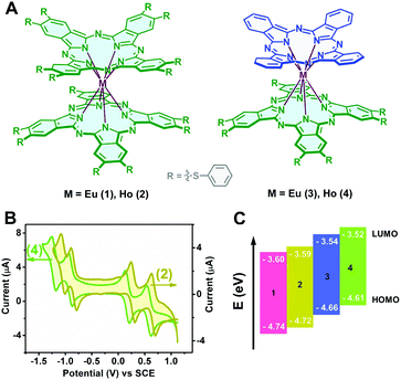 |
| | Fig. 1 (A) Schematic molecular structures of the bis(phthalocyaninato)lanthanide(III) complexes 1–4; (B) cyclic voltammetry of Ho[Pc(SPh)8]2 (2) and Ho(Pc)[Pc(SPh)8] (4) in CH2Cl2 containing 0.1 M [NBu4][ClO4] at a scan rate of 20 mV s−1 and (C) comparison of the HOMO and LUMO energy levels of 1–4. | |
Results and discussion
Electrochemistry
The HOMO (highest occupied molecular orbital) and LUMO (lowest unoccupied molecular orbital) energy levels relative to those of the working electrode are crucial in determining the majority charge carrier and charge carrier stability in typical organic semiconductors.40,41 The electrochemical properties of a series of double-deckers 1–4 were characterized using cyclic voltammetry (CV). Fig. 1B shows the cyclic voltammograms of 2 and 4 as typical representatives. As can be seen, within the electrochemical window of CH2Cl2, these double-deckers show one one-electron oxidation labelled as Oxd1 and three one-electron reductions (Red1–Red3), Table S1 (ESI†). As expected, along with a decrease in the number of electron withdrawing thiophenoxy groups from M[Pc(SPh)8]2 to M(Pc)[Pc(SPh)8], the half-wave potentials (vs. SCE) for both the first oxidation (Oxd1) and the first, second, and third reductions (Red1–Red3) are distinctly shifted to the more negative direction.42–48 On the basis of the first and second reductions (vs. SCE) of these compounds,31,43 the HOMO energies are estimated to range from −4.74 (1), to −4.72 (2), −4.66 (3), and −4.61 eV (4), while the LUMO energies amount to −3.60 (1), −3.59 (2), −3.54 (3), and −3.52 eV (4), as shown in Fig. 1C and Table S1 (ESI†), suggesting the intrinsic ambipolar semiconductor nature of the series of double-decker complexes with an enhanced air stability of 1 and 2 relative to 3 and 4 on the basis of previous investigation results.49,50 It is noteworthy that the HOMO and LUMO energy levels measured by cyclic voltammetry only represent the data for an individual molecule, which might be higher compared with those in the solid state due to the electronic coupling between the neighbouring molecules in the solid state.44,51,52 Therefore, ultraviolet photoelectron spectrometry (UPS) measurement was carried out for the self-assembled nanostructures of 1–4 (named as aggregates 1–4), Fig. S1 (ESI†). As expected, the lower HOMO energy levels of −5.18 (1), −5.07 (2), −4.71 (3), and −4.62 eV (4) than those obtained in solution were indeed derived on the basis of the UPS results for the aggregates. In addition, along with the increase in the number of thiophenoxy groups from M(Pc)[Pc(SPh)8] (3, 4) to M[Pc(SPh)8]2 (1, 2), the energy gap of EHOMO − Ef (Fermi level) becomes obviously larger, Fig. S1 (ESI†), equivalent to a larger shift of Ef towards the LUMO level from 3 and 4 to 1 and 2, revealing the generation of much more free electrons53 and a more effective n-type semiconducting nature of the aggregates 1 and 2vs.3 and 4.
OFET device performance
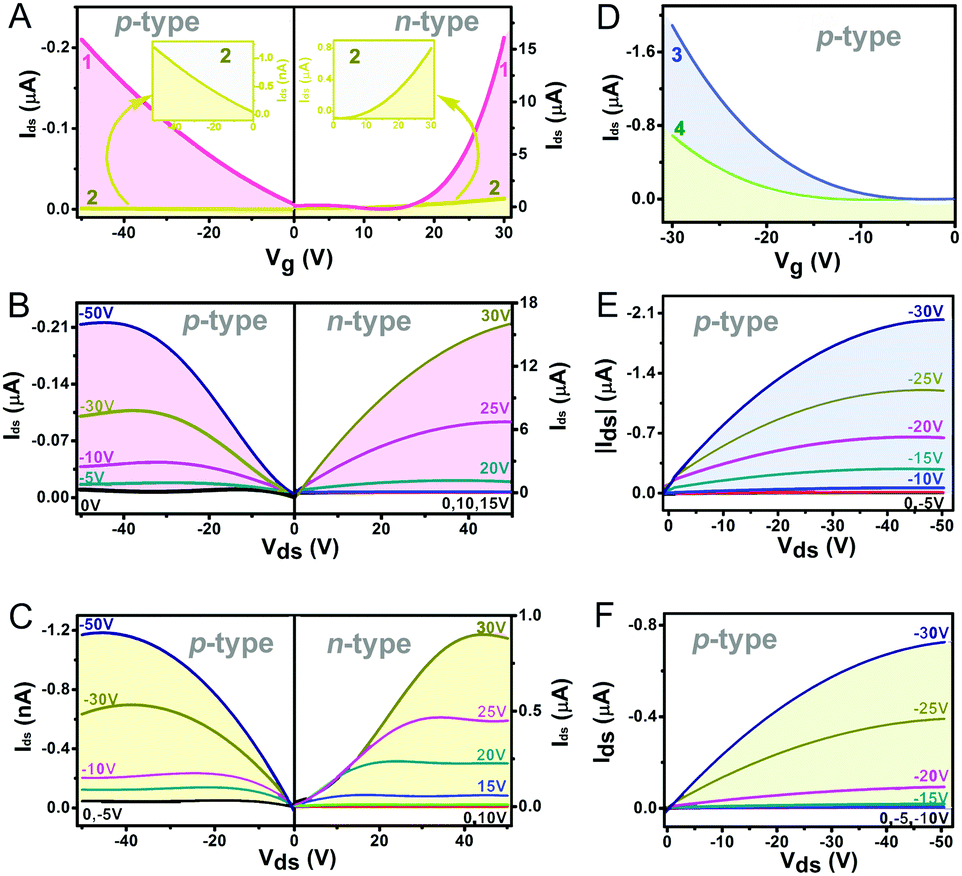
Organic field effect transistors (OFETs) provide a simple device structure that allows detailed analysis of material charge transport characteristics via evaluation of the current–voltage response upon the application of a negative or positive gate-source bias.41 As a consequence, the nanostructures self-assembled from 1–4 using a solution-based quasi-Langmuir–Shäfer (QLS) method54 have been fabricated into OFET devices on a hexamethyldisilazane (HMDS)-treated substrate. As summarized in Table 1 and shown in Fig. 2A and B, the devices based on the self-assembled nanostructures of the homoleptic double decker 1 present carrier mobility not only for holes but also for electrons with an average value of 1.1 × 10⁻⁴ cm2 V−1 s−1 in air and 0.11 cm2 V−1 s−1 in N2, respectively, revealing the typical ambipolar semiconductor nature of this compound. This is also true for the devices fabricated from homoleptic analogue 2 but with significantly lower hole and electron mobilities as low as 4.9 × 10⁻⁷ and 3.0 × 10⁻³ cm2 V−1 s−1 (Table 1 and Fig. 2A, C), respectively, related mainly to the lower intermolecular interactions and molecular ordering/packing of the aggregates of 2 than those of 1 (vide infra). It is worth noting that the n-type OFET characteristics of the aggregates 1 and 2 could be detected only under an inert N2 atmosphere, indicating that the LUMO energies of 1 and 2 in the aggregates still do not meet the energy required for an air-stable n-type OFET (ELUMO < −4.0 eV) against air-derived electron traps.40,55 Furthermore, the measurements of the device performance disclosed the only p-type characteristics for aggregates 3 and 4 in both air and N2 atmosphere with a carrier mobility for holes of up to 4.4 × 10⁻³ and 2.6 × 10⁻³ cm2 V−1 s−1, respectively, Fig. 2D–F and Table 1. As can be seen, despite the intrinsic ambipolar semiconducting properties of 3 and 4 suggested by their electrochemical results, the n-channel behavior was not detected on the devices even in N2. This should attributed to the large Mott–Schottky barrier resulting from the mismatching between their relatively high LUMO levels (∼−3.54 and −3.52 eV) and the Fermi level of the Au electrode (−4.8 to −5.1 eV).15
Table 1 Electrical properties and NH3-sensing behaviours of the self-assembled aggregates of compounds 1–4
| Compounds |
μ
h (cm2 V−1 s−1) |
μ
e (cm2 V−1 s−1) |
σ (S cm−1) |
n
h (cm−3) |
n
e (cm−3) |
Response type |
Sensitivity (%ppm−1) |
| 15–100 ppm |
100–800 ppm |
| Eu[Pc(SPh)8]2 (1) |
1.1 × 10⁻⁴ |
0.11 |
6.4 × 10⁻⁵ |
3.6 × 10¹⁸ |
3.6 × 10¹⁵ |
n |
0.022 |
0.011 |
| Ho[Pc(SPh)8]2 (2) |
4.9 × 10⁻⁷ |
3.0 × 10⁻³ |
4.7 × 10⁻⁵ |
6.0 × 10²⁰ |
9.8 × 10¹⁶ |
n |
0.011 |
0.0054 |
| EuPc[Pc(SPh)8] (3) |
4.4 × 10⁻³ |
N/A |
2.0 × 10⁻⁴ |
2.8 × 10¹⁷ |
N/A |
p |
−0.0083 |
−0.0029 |
| HoPc[Pc(SPh)8] (4) |
2.6 × 10⁻³ |
N/A |
1.0 × 10⁻⁴ |
2.4 × 10¹⁷ |
N/A |
p |
−0.019 |
−0.0053 |
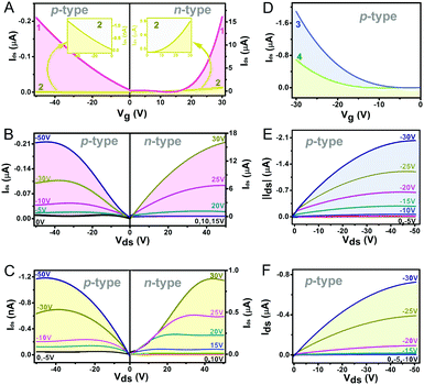 |
| | Fig. 2 Transfer plots (A and D) and output plots (B and C, and E and F) for OFETs fabricated from the aggregates 1 (A and B), 2 (A and C), 3 (D and E), and 4 (D and F), respectively, on the HMDS-treated SiO2/Si substrates. | |
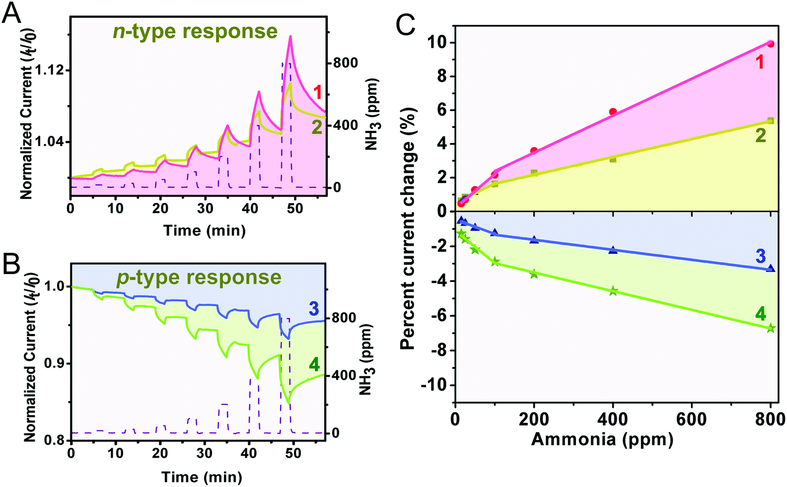
NH3 sensing nature and sensitivity
To assess the applicability in chemical gas sensing of the four double-deckers, devices made of the aggregates 1–4 were exposed to different concentrations of the electron-donating gas NH3 (15–800 ppm) diluted by an argon atmosphere, with a duty cycle where the dynamic exposure period is fixed at 2 min and the recovery period is fixed at 5 min. The electrical responses recorded at room temperature for the four sensors at different NH3 concentrations are compared in Fig. 3A and B, where the time-dependent current plots were normalized at t = 0 s. As can be found, during the exposure period the devices of the aggregates 1 and 2 exhibit a positive response to the electron-donating NH3, and therefore behave as an n-type semiconductor.56,57 This is in good contrast to the negative response of the devices of the aggregates 3 and 4 and their p-type semiconductor behaviour. This indicates the effect of the number of peripheral electron-withdrawing thiophenoxy substituents on the response nature upon chemical doping by electron donating NH3, in line with previous findings.29,57,58 Furthermore, the current change (in percentage) was calculated for each concentration accordingly, current change (%) = [(I0 − If)/I0] × 100, where I0 is the current value at the beginning of an exposure/recovery cycle and If is the current value at the end of the 2 min exposure period. As can be seen in Fig. 3C, all the sensors of 1–4 respond linearly to the concentration of NH3 in the range of both 15–100 ppm and 100–800 ppm (Adj. R-square > 0.97), suggesting the good application potential of this kind of sensor in quantitatively analyzing NH3. The slope of the linear fit for the current change in percentage versus NH3 concentration (% ppm−1, defined as sensitivity) is about 0.022, 0.011, −0.0083, and −0.019 in the range of 15–100 ppm, and 0.011, 0.0054, −0.0029, and −0.0053 in the range of 100–800 ppm, for 1, 2, 3, and 4, respectively, Fig. 3C and Table 1. Obviously, aggregates 1–4 are more sensitive towards NH3 with a low concentration range of 15–100 ppm, which is actually the range encountered in practical industrial waste control (10–100 ppm),14 confirming again their potential practical application as industrial NH3 sensors and/or detectors. It is clear that the n-type responses of aggregates 1 and 2 are more sensitive towards NH3 than the p-type responses of aggregates 3 and 4. Furthermore, along with the increase of the metal ion radius from Ho in 2 to Eu in 1, the sensitivity gets increased by a factor of ca. 2 for the n-type response, which however conversely gets decreased by a factor of ca. 2 for the p-type response from aggregate 4 to 3. For aggregate 1, a close-packing molecular architecture with highly ordered nanostructures as detailed below is believed to be able to provide more effective adsorption sites for NH3 and in turn yield a large modulation in current (i.e. the highest sensitivity) in the homoleptic series (1 and 2), actually the highest one among these aggregates 1–4.59 This, however, is not the case for the heteroleptic aggregate 3. Despite the higher hole mobility and stronger inter-molecular interaction (resulting from an increased metal ion radius) relative to aggregate 4, aggregate 3 still exhibits low sensitivity towards NH3, actually the lowest one among these four aggregates.
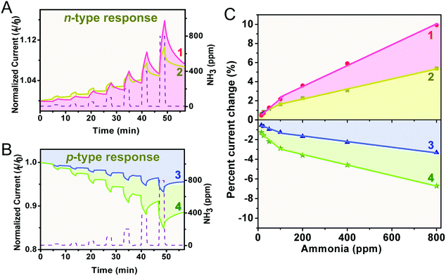 |
| | Fig. 3 The time-dependent current plots exposed to NH3 at various concentrations in the range of 15–800 ppm for the aggregates 1–2 (A) and 3–4 (B); the sensor response varies linearly with the NH3 concentration in the range of 15–800 ppm for the aggregates 1–4 (C). | |
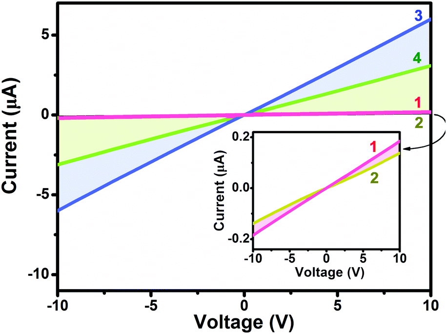
Electrical conductivity
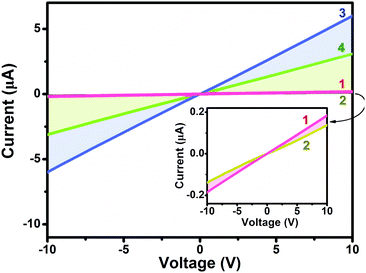
Towards clarifying the significantly different gas sensing behavior [in terms of both the response nature (p- or n-type) and sensing sensitivity] between heteroleptic and homoleptic double-deckers as well that between the Ho and Eu counterparts within the respective series, the electrical conductivity of the aggregates 1–4 was evaluated based on a current–voltage (I–V) measurement, Fig. 4. In air, the four devices fabricated from aggregates 1–4 exhibit a similar Ohmic behavior at a low bias voltage of 10 V with the current values of 1.9 × 10⁻⁷, 1.4 × 10⁻⁷, 6.0 × 10⁻⁶, and 3.1 × 10⁻⁶ A for aggregate 1, 2, 3, and 4, respectively. The conductivity (σ) is therefore estimated to be ca. 6.4 × 10⁻⁵, 4.7 × 10⁻⁵, 2.0 × 10⁻⁴, and 1.0 ×10⁻⁴ S cm−1, respectively, Table 1.60 Obviously, the electrical conductivity gets decreased by one order of magnitude along with an increase in the peripheral substituent number from eight in M(Pc)[Pc(SPh)8] for 3 and 4 to sixteen in M[Pc(SPh)8]2 for 1 and 2 associated with the electron-withdrawing thiophenoxy group effect.31,42 This trend in performance is consistent with the previously reported electrical behaviour of MPc and MPcF16 (M = Cu, Zn) films since the addition of electron-withdrawing substituents on a metallo phthalocyanine macrocycle decreases the electron density of the conjugated cycle and increases the oxidation potential of the macrocycle.57,61–63 In addition, the conductivity of aggregate 3 of Eu(Pc)[Pc(SPh)8] is about two times higher than that of aggregate 4 of Ho(Pc)[Pc(SPh)8] due to the larger ionic radius as detailed below. This is also true for 1vs.2 in the corresponding devices.
 |
| | Fig. 4 Representative I–V characteristics of the aggregates of 1–4. | |
Lower density charge carrier makes sense
Based on the carrier mobility μ (μh for hole and μe for electron) and conductivity σ, following the equation σ = neμ (where n and e stand for the density of the charge carrier and elementary charge, respectively), the charge carrier density for holes and/or electrons for aggregates 1–4 can be calculated and the results are listed in Table 1. As summarized in Table 1, the original carrier densities of electrons (ne) and holes (nh) amount to 3.6 × 10¹⁵ and 3.6 × 1018 cm−3 for 1, and 9.8 × 10¹⁶ and 6.0 × 1020 cm−3 for 2, respectively. Obviously, the original electron density (ne) for both aggregates is about three orders of magnitude lower than their respective hole density (nh). Interestingly, this lower density of charge carriers determines their sensing nature, causing these two ambipolar double-deckers 1 and 2 to show an n-type rather than a p-type response towards NH3. This seems quite strange at first glance; however, it could be easily rationalized on the basis of the higher mobility of electrons for both aggregates 1 and 2versus that of holes due to the well-known natural phenomenon: the higher the charge transporting speed, the easier it is for it to be affected upon external perturbation. Nevertheless, within these two n-type NH3 sensors, aggregate 1 possessing lower original electron density (ne) but higher electron transporting speed relative to aggregate 2 was revealed to exhibit higher sensitivity. As a consequence, for the ambipolar organic semiconductor gas sensors, first the lower density of the original carrier (hole versus electron) determines the response nature (n- versus p-type). Second, the lower density carrier in the same series determines the higher sensing sensitivity. Additional support for this point comes from the NH3 sensing performance of aggregates 3 and 4.
As can be found, the original hole density (nh) for the p-type sensor of aggregate 3 is 2.8 × 1017 cm−3, while the one for the same p-type sensor of aggregate 4 amounts to 2.4 × 1017 cm−3. Obviously, the lower original hole density in aggregate 4 is responsible for the higher sensitivity towards NH3 than aggregate 3, disclosing again the key role of the original carrier (here the hole) density in determining the gas sensing sensitivity: the lower the original carrier density in the device, the faster the charge transporting speed, the easier it is for it to be affected upon external doping, and the higher the gas sensing sensitivity. It is worth noting that someone might claim the higher hole mobility for aggregate 3 over that of 4 as shown in Table 1. This however is rationalized on the basis of the higher relative hole mobility (μr) for aggregate 4versus that of 3 (μr = μh4/μh3 = 1.17) after normalization of the conductivity.
Microstructures and morphologies
Towards clarifying the relationship between the electrical properties (i.e. carrier mobility and conductivity) and microstructures of aggregates 1–4, analysis of the molecular packing mode of the double-decker molecules and the internal structure in these aggregates was carried out on the basis of UV-vis spectroscopy, XRD measurement, and AFM observations. As shown in Fig. S2 and summarized in Table S1 (ESI†), the double-decker compound in CH2Cl2 solution shows an intense Q-band at 716, 709, 694 and 688 nm for 1, 2, 3, and 4, respectively. As a result, the main Q band is blue-shifted by 7 nm from 1 to 2, and 6 nm from 3 to 4, implying a stronger face-to-face intra-molecular interaction along with the decrease in ionic radius from Eu to Ho. After being fabricated into the aggregates, the main Q band red-shifts to 730, 719, 702 and 691 nm, indicating the formation of a J aggregate (edge-to-edge) depending on the dominant side-group interaction in cooperation with the π–π interaction among the double-decker molecules. The main Q band gets red-shifted by 14 and 10 nm for 1 and 2, as well as 8 and 3 nm for 3 and 4, compared to the respective monomeric state in solution. Consequently, the degree of red-shift gets increased from 2 to 1, and also from 4 to 3, indicating a larger edge-to-edge inter-molecular interaction along with an increased metal ionic radius from Ho to Eu. Furthermore, a more significant red-shift in the main Q band occurs for the homoleptic double-deckers 1 and 2 (red-shifted by 14 and 10 nm) involving sixteen peripheral thiophenoxy groups than for the heteroleptic double-deckers 3 and 4 involving eight peripheral substituents (red-shifted by 8 and 3 nm). This suggests the increased population of the molecular transition dipoles arranged in a head-to-tail fashion from 4 and 3 to 2 and 1 in these aggregates and the contribution of aggregation to the LUMO energetic stabilization of the double-decker materials in the solid state.44
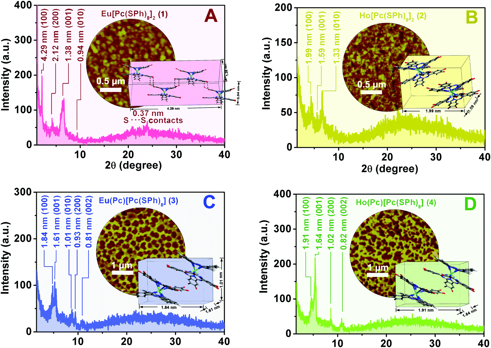
Fig. 5 shows the XRD patterns of the self-assembled aggregates 1–4. In the XRD diagram of aggregate 1, significantly intensified and sharpened diffractions were observed at 4.29, 1.38, and 0.94 nm, which are ascribed to the diffractions from the (100), (001), and (010) planes, respectively,34Fig. 5A. According to the single crystal X-ray diffraction analysis result of the double-decker counterpart Eu[Pc(OPh)8]2,64 a parallelepiped lattice consisting of four Eu[Pc(SPh)8]2 molecules with the cell parameters of 4.29 nm (length) × 1.38 nm (width) × 0.94 nm (thickness) formed from the edge-to-edge (J-type) stacking of the four double-decker molecules, is therefore constructed for aggregate 1, the inset of Fig. 5A. More importantly, the observation of one additional high-order diffraction at 0.37 nm for aggregate 1, which is just equal to twice the van der Waals radius of a sulfur atom, reveals the formation of S–S bonding between the sulfur atoms of the adjacent Eu[Pc(SPh)8]2 molecules.58,65 Meanwhile, the appearance of the higher-order diffraction at 2.12 nm due to the (200) plane in the XRD pattern of aggregate 1 confirms again the more favorable molecular packing and in turn long-range periodicity along the [100] direction in this aggregate. This, however, is not the case for aggregate 2. As shown in Fig. 5B, the well-defined Bragg peaks in the XRD pattern of aggregate 2 are observed at 1.99, 1.59, and 1.33 nm due to the (100), (001), and (010) planes,42 resulting in a unit cell only consisting of two Ho[Pc(SPh)8]2 molecules from a parallelepiped lattice with the cell parameters of 1.99 nm (length) × 1.59 nm (width) × 1.33 nm (thickness), the inset of Fig. 5B. In comparison with those of aggregate 2, the a slightly smaller thickness and a significantly enlarged length in one unit cell for aggregate 1 suggest the stronger intermolecular interactions along the vertical and parallel directions to the phthalocyanine ring between the adjacent double-decker molecules depending on the intermolecular S–S bonding and π–π interaction as well as van der Waals interactions. These lead to higher molecular ordering and enhanced crystallinity in aggregate 1 and thus to its higher carrier mobilities of both holes (μh) and electrons (μe) as well as better conductivity (σ) revealed in comparison with those for aggregate 2 as detailed above. In the XRD pattern of aggregate 3, the diffraction peaks observed at 1.84, 1.61 and 1.01 nm are attributed to the diffractions from the (100), (001) and (010) planes, respectively, resulting in a unit cell with the dimensional size of 1.84 nm (length) × 1.61 nm (width) × 1.01 nm (thickness), formed from the edge-to-edge (J-type) stacking of two double-decker molecules depending on the intermolecular π–π interaction and van der Waals interactions, Fig. 5C. In addition, the observation of two additional higher-order diffractions at 0.93 and 0.81 nm for aggregate 3, corresponding to the (200) and (002) planes, seems to indicate the relatively high molecular-ordering of this nanostructure along the [100] and [001] directions. This is also true for aggregate 4, Fig. 5D. The slightly larger unit cell with dimension parameters of 1.91 nm (length) × 1.64 nm (width) derived for aggregate 4 than for 3, the inset of Fig. 5D, however, suggests a smaller degree of intermolecular thiophenoxy side group interdigitation for 4 than 3. The denser molecular packing in aggregate 3 is certainly responsible for its higher carrier mobility for holes (μh) and conductivity (σ) revealed in comparison with those for aggregate 4. These results are fully consistent with the results of the electronic absorption spectroscopic study.
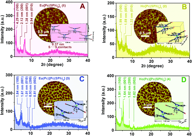 |
| | Fig. 5 XRD profiles of the self-assembled aggregates 1–4 (A–D) and the corresponding schematic molecular arrangement of 1–4 in the self-assembled aggregates (insets of A–D). The dashed lines in the inset of A indicate S⋯S contact of 0.37 nm in aggregate 1; AFM images of the self-assembled aggregates 1–4 (also the insets of A–D). | |
The AFM observations of aggregates 1–4 reveal a distinct different microstructure between the aggregates of M[Pc(SPh)8]2 (1, 2) and M(Pc)[Pc(SPh)8] (3, 4), the insets of Fig. 5. Aggregate 1 shows fairly uniform crystalline grains and fine connectivity with an average diameter of ca. 300 nm, the inset of Fig. 5A, which is surely closely related with the S–S bonding interaction in addition to the larger van der Waals force in solid state packing between the neighbouring Eu[Pc(SPh)8]2 molecules. As shown in the inset of Fig. 5B, aggregate 2 comprises small grains/domains approximately 50–200 nm in diameter together with some gaps and cracks between the aggregate domains. Obviously, a stronger intermolecular interaction for aggregate 1 in turn results in a larger extent of ordered molecular packing and larger domain size in the solid state, which then contribute to the significant increase in the carrier mobility and gas sensing sensitivity of the corresponding devices. Interestingly, decrease in the thiophenoxy substituent number from sixteen in M[Pc(SPh)8]2 to eight in M(Pc)[Pc(SPh)8] induces a significant change in the aggregate surface morphology. As can be seen from the insets of Fig. 5C and D, aggregate 3 displays a uniform nest-like structure with an average cell diameter of ca. 300 nm and wall thickness of ca. 150 nm, while aggregate 4 exhibits a nest-like morphology composed of a large number of long and flexible nanofibrils ca. 100–200 nm in width. More uniform-sized nano-nests were achieved for aggregate 3 relative to those of 4 because of the enhanced intermolecular interactions as detailed above, which then led to fewer traps and/or defects around the cell boundaries in aggregate 3 and thus contributed to improving its electrical conductivity and carrier mobility.
Conclusions
Systematic studies on the OFET performance, conductivity, and NH3-sensing properties of the self-assembled nanostructures fabricated from the ambipolar bis(phthalocyaninato) rare earth complexes in a combinative manner clearly unravel the key role of low density carriers (hole versus electron) in determining both the gas sensing response nature (p- or n-type) and the sensing sensitivity of ambipolar organic semiconductors for reducing gas NH3. Additional support comes from the sensing behavior of the p-type organic semiconductor in terms of the sensing sensitivity. The present result will be surely helpful towards clarifying the sensing nature of organic semiconductors.
Conflicts of interest
There are no conflicts to declare.
Acknowledgements
This work was financially supported by the National Key Basic Research Program of China (No. 2013CB933402), the National Natural Science Foundation of China (No. 21771192, 21371073, 21301017, 21631003, and 21671017), the Natural Science Foundation of Shandong Province (ZR2017ZB0315), the Taishan Scholar Foundation (ts201511019) and the Research Foundation from China University of Petroleum (East China) (Y1510051).
Notes and references
- Z. Wang, L. Huang, X. Zhu, X. Zhou and L. Chi, Adv. Mater., 2017, 29, 1703192 CrossRef PubMed.
- B. Wang, T. P. Huynh, W. Wu, N. Hayek, T. T. Do, J. C. Cancilla, J. S. Torrecilla, M. M. Nahid, J. M. Colwell, O. M. Gazit, S. R. Puniredd, C. R. McNeill, P. Sonar and H. Haick, Adv. Mater., 2016, 28, 4012–4018 CrossRef CAS PubMed.
- O. Voznyy, B. R. Sutherland, A. H. Ip, D. Zhitomirsky and E. H. Sargent, Nat. Rev. Mater., 2017, 2, 17026 CrossRef CAS.
- Y. Li, T. Liu, H. Liu, M. Tian and Y. Li, Acc. Chem. Res., 2014, 47, 1186–1198 CrossRef CAS PubMed.
- H. Liu, J. Xu, Y. Li and Y. Li, Acc. Chem. Res., 2010, 43, 1496–1508 CrossRef CAS PubMed.
- C. Zhang, P. Chen and W. Hu, Chem. Soc. Rev., 2015, 44, 2087–2107 RSC.
- H. Jeong, D. Kim, D. Xiang and T. Lee, ACS Nano, 2017, 11, 6511–6548 CrossRef CAS PubMed.
- M. Segev-Bar and H. Haick, ACS Nano, 2013, 7, 8366–8378 CrossRef CAS PubMed.
- J. Kong, N. R. Franklin, C. Zhou, M. G. Chapline, S. Peng, K. Cho and H. Dai, Science, 2000, 287, 622–625 CrossRef CAS PubMed.
- G. Lu, K. Yu, L. E. Ocola and J. Chen, Chem. Commun., 2011, 47, 7761–7763 RSC.
- B. Xu, M. Zhu, W. Zhang, X. Zhen, Z. Pei, Q. Xue, C. Zhi and P. Shi, Adv. Mater., 2016, 28, 3333–3339 CrossRef CAS PubMed.
- H. Wang, X. Kong, S. Zhao, J. Wu, X. Li and Y. Chen, New J. Chem., 2017, 41, 11955–11961 RSC.
- K. Abdullah, Y. Wu, S. Zhao, X. Kong, X. Li and Y. Chen, Inorg. Chem. Commun., 2017, 86, 1–5 CrossRef CAS.
- X. Kong, Z. Dong, Y. Wu, X. Li, Y. Chen and J. Jiang, Chin. J. Chem., 2016, 34, 975–982 CrossRef CAS.
- J. Zaumseil and H. Sirringhaus, Chem. Rev., 2007, 107, 1296–1323 CrossRef CAS PubMed.
- E. J. Meijer, D. M. de Leeuw, S. Setayesh, E. van Veenendaal, B.-H. Huisman, P. W. M. Blom, J. C. Hummelen, U. Scherf and T. M. Klapwijk, Nat. Mater., 2003, 2, 678–682 CrossRef CAS PubMed.
- R. K. Paul, S. Badhulika, N. M. Saucedo and A. Mulchandani, Anal. Chem., 2012, 84, 8171–8178 CrossRef CAS PubMed.
- S. Mao, S. Cui, G. Lu, K. Yu, Z. Wen and J. Chen, J. Mater. Chem., 2012, 22, 11009–11013 RSC.
- C. D. Dimitrakopoulos and P. R. L. Malenfant, Adv. Mater., 2002, 14, 99–117 CrossRef CAS.
- G. Horowitz, Adv. Mater., 1998, 10, 365–377 CrossRef CAS.
- H. Sirringhaus, Adv. Mater., 2005, 17, 2411–2425 CrossRef CAS.
- R. Li, W. Hu, Y. Liu and D. Zhu, Acc. Chem. Res., 2010, 43, 529–540 CrossRef CAS PubMed.
- H. Usta, A. Facchetti and T. J. Marks, Acc. Chem. Res., 2011, 44, 501–510 CrossRef CAS PubMed.
- L. Valli, Adv. Colloid Interface Sci., 2005, 116, 13–44 CrossRef CAS PubMed.
- W. Wu, Y. Liu and D. Zhu, Chem. Soc. Rev., 2010, 39, 1489–1502 RSC.
- R. P. Ortiz, A. Facchetti and T. J. Marks, Chem. Rev., 2010, 110, 205–239 CrossRef CAS PubMed.
- S. Liu, W. M. Wang, A. L. Briseno, S. C. B. Mannsfeld and Z. Bao, Adv. Mater., 2009, 21, 1217–1232 CrossRef CAS.
- Y. Wang, Y. Chen, R. Li, S. Wang, X. Li and J. Jiang, Langmuir, 2007, 23, 5836–5842 CrossRef CAS PubMed.
- T. Sizun, M. Bouvet, Y. Chen, J. M. Suisse, G. Barochi and J. Rossignol, Sens. Actuators, B, 2011, 159, 163–170 CrossRef CAS.
- J. H. Zagal, S. Griveau, J. F. Silva, T. Nyokong and F. Bedioui, Coord. Chem. Rev., 2010, 254, 2755–2791 CrossRef CAS.
- Y. Chen, D. Li, N. Yuan, J. Gao, R. Gu, G. Lu and M. Bouvet, J. Mater. Chem., 2012, 22, 22142–22149 RSC.
- Y. Chen, W. Su, J. Jiang, X. Li and Y. Liu, J. Am. Chem. Soc., 2005, 127, 15700–15701 CrossRef CAS PubMed.
- J. Kan, Y. Chen, D. Qi, Y. Liu and J. Jiang, Adv. Mater., 2012, 24, 1755–1758 CrossRef CAS PubMed.
- D. Gao, X. Zhang, X. Kong, Y. Chen and J. Jiang, ACS Appl. Mater. Interfaces, 2015, 7, 2486–2493 CAS.
- X. Kong, X. Zhang, D. Gao, D. Qi, Y. Chen and J. Jiang, Chem. Sci., 2015, 6, 1967–1972 RSC.
- G. Lu, X. Kong, P. Ma, K. Wang, Y. Chen and J. Jiang, ACS Appl. Mater. Interfaces, 2016, 8, 6174–6182 CAS.
- D. Li, H. Wang, J. Kan, Y. Chen and J. Jiang, Org. Electron., 2013, 14, 2582–2589 CrossRef CAS.
- T. Ye, T. Takami, R. Wang, J. Jiang and P. S. Weiss, J. Am. Chem. Soc., 2006, 128, 10984–10985 CrossRef CAS PubMed.
- T. Takami, T. Ye, B. K. Pathem, D. P. Arnold, K. Sugiura, Y. Bian, J. Jiang and P. S. Weiss, J. Am. Chem. Soc., 2010, 132, 16460–16466 CrossRef CAS PubMed.
- B. A. Jones, A. Facchetti, M. R. Wasielewski and T. J. Marks, J. Am. Chem. Soc., 2007, 129, 15259–15278 CrossRef CAS PubMed.
- A. Facchetti, M. Mushrush, M.-H. Yoon, G. R. Hutchison, M. A. Ratner and T. J. Marks, J. Am. Chem. Soc., 2004, 126, 13480–13501 CrossRef CAS PubMed.
- G. Lu, M. Bai, R. Li, X. Zhang, C. Ma, P.-C. Lo, D. K. P. Ng and J. Jiang, Eur. J. Inorg. Chem., 2006, 3703–3709 CrossRef CAS.
- P. Zhu, F. Lu, N. Pan, D. P. Arnold, S. Zhang and J. Jiang, Eur. J. Inorg. Chem., 2004, 510–517 CrossRef CAS.
- R. Murdey, M. Bouvet, M. Sumimoto, S. Sakaki and N. Sato, Synth. Met., 2009, 159, 1677–1681 CrossRef CAS.
- Z. Bao, A. Lovinger and J. Brown, J. Am. Chem. Soc., 1998, 120, 207–208 CrossRef CAS.
- M. L. Tang, J. H. Oh, A. D. Reichardt and Z. Bao, J. Am. Chem. Soc., 2009, 131, 3733–3740 CrossRef CAS PubMed.
- D. Schlettwein, D. Wohrle, E. Karmann and U. Melville, Chem. Mater., 1994, 6, 3–6 CrossRef CAS.
- P. Ma, J. Kan, Y. Zhang, C. Hang, Y. Bian, Y. Chen, N. Kobayshi and J. Jiang, J. Mater. Chem., 2011, 21, 18552–18559 RSC.
- M. L. Tang, A. D. Reichardt, P. Wei and Z. Bao, J. Am. Chem. Soc., 2009, 131, 5264–5273 CrossRef CAS PubMed.
- C. R. Newman, C. D. Frisbie, D. A. da Silva Filho, J.-L. Brédas, P. C. Ewbank and K. R. Mann, Chem. Mater., 2004, 16, 4436–4451 CrossRef CAS.
- J. L. Brédas, D. Beljonne, V. Coropceanu and J. Cornil, Chem. Rev., 2004, 104, 4971–5004 CrossRef PubMed.
- J. L. Brédas, Mater. Horiz., 2014, 1, 17–19 RSC.
- K. Shi, Z. Lu, Z. Yu, H. Liu, Y. Zou, C. Yang, Y. Dai, Y. Lu, J. Wang and J. Pei, Adv. Electron. Mater., 2017, 1700164 CrossRef.
- Y. Chen, M. Bouvet, T. Sizun, Y. Gao, C. Plassard, E. Lesniewska and J. Jiang, Phys. Chem. Chem. Phys., 2010, 12, 12851–12861 RSC.
- Z. Wang, C. Kim, A. Facchetti and T. J. Marks, J. Am. Chem. Soc., 2007, 129, 13362–13363 CrossRef CAS PubMed.
- V. Parra, M. Bouvet, J. Brunet, M. L. Rodríguez-Méndez and J. A. de Saja, Thin Solid Films, 2008, 516, 9012–9019 CrossRef CAS.
- V. Parra, J. Brunet, A. Pauly and M. Bouvet, Analyst, 2009, 134, 1776–1778 RSC.
- B. A. Minch, W. Xia, C. L. Donley, R. M. Hernandez, C. Carter, M. D. Carducci, A. Dawson, D. F. O’Brien and N. R. Armstrong, Chem. Mater., 2005, 17, 1618–1627 CrossRef CAS.
- M. Bora, D. Schut and M. A. Baldo, Anal. Chem., 2007, 79, 3298–3303 CrossRef CAS PubMed.
- A. W. Snow and H. Wohltjen, Chem. Mater., 1998, 10, 947–949 CrossRef CAS.
- Z. J. Bao, A. Lovinger and A. Dodabalapur, Appl. Phys. Lett., 1996, 69, 3066–3068 CrossRef CAS.
- D. G. De Oteyza, E. Barrena, J. O. Osso, S. Sellner and H. Dosch, J. Am. Chem. Soc., 2006, 128, 15052–15053 CrossRef CAS PubMed.
- R. Murdey, N. Sato and M. Bouvet, Mol. Cryst. Liq. Cryst., 2006, 455, 211–218 CrossRef CAS.
- M. L. Rodríguez-Méndez, Y. Gorbunova and J. A. de Saja, Langmuir, 2002, 18, 9560–9565 CrossRef.
-
Handbook of Liquid Crystals, ed. D. Demus, J. Goodby, G. W. Gray and H.-W. Spiess, Fundamentals, Wiley-VCH, New York, 1998, vol. 1 Search PubMed.
Footnote |
| † Electronic supplementary information (ESI) available: UPS spectra of the self-assembled aggregates of 1–4. UV-vis absorption spectra of 1–4 in dichloromethane solution and self-assembled aggregates. Half-wave redox potentials of 1–4 (V vs. SCE) in CH2Cl2 containing 0.1 M TBAP and the maximum Q band absorption of compounds 1–4 in CH2Cl2 solution and self-assembled nanostructures. See DOI: 10.1039/c7qm00607a |
|
| This journal is © the Partner Organisations 2018 |
Click here to see how this site uses Cookies. View our privacy policy here. 
 *a,
Xia
Kong
a,
Guifen
Lu
*a,
Xia
Kong
a,
Guifen
Lu