
Wafer scale growth of single crystal two-dimensional van der Waals materials
Chetna
Gautam
 a,
Baishali
Thakurta
b,
Monalisa
Pal
b,
Anup Kumar
Ghosh
*a and
Anupam
Giri
*c
a,
Baishali
Thakurta
b,
Monalisa
Pal
b,
Anup Kumar
Ghosh
*a and
Anupam
Giri
*c
aDepartment of Physics, Institute of Science, Banaras Hindu University, Varanasi, UP – 221005, India. E-mail: akghosh@bhu.ac.in; anupamgiri@allduniv.ac.in
bDepartment of Chemistry, Institute of Science, Banaras Hindu University, Varanasi, UP – 221005, India
cDepartment of Chemistry, Faculty of Science, University of Allahabad, Prayagraj, UP-211002, India
First published on 22nd February 2024
Abstract
Two-dimensional (2D) van der Waals (vdW) materials, including graphene, hexagonal boron nitride (hBN), and metal dichalcogenides (MCs), form the basis of modern electronics and optoelectronics due to their unique electronic structure, chemical activity, and mechanical strength. Despite many proof-of-concept demonstrations so far, to fully realize their large-scale practical applications, especially in devices, wafer-scale single crystal atomically thin highly uniform films are indispensable. In this minireview, we present an overview on the strategies and highlight recent significant advances toward the synthesis of wafer-scale single crystal graphene, hBN, and MC 2D thin films. Currently, there are five distinct routes to synthesize wafer-scale single crystal 2D vdW thin films: (i) nucleation-controlled growth by suppressing the nucleation density, (ii) unidirectional alignment of multiple epitaxial nuclei and their seamless coalescence, (iii) self-collimation of randomly oriented grains on a molten metal, (iv) surface diffusion and epitaxial self-planarization and (v) seed-mediated 2D vertical epitaxy. Finally, the challenges that need to be addressed in future studies have also been described.
 Chetna Gautam | Chetna Gautam received her B.Sc. degree in physics from Choudhary Charan Singh University (India) in 2016 and M.Sc. degree in applied physics from Babasaheb Bhimrao Ambedkar University (India) in 2018. She is pursuing her Ph.D. degree under the supervision of Prof. Anup Kumar Ghosh in physics at Banaras Hindu University (India). Her research interests include the synthesis of 2D transition metal dichalcogenides and their optoelectronic applications. |
 Baishali Thakurta | Baishali Thakurta received her B.Sc. degree in chemistry from the University of Calcutta, India, in 2015 and M. Sc. degree in analytical chemistry from Jadavpur University, India, in 2019. She is pursuing her Ph.D. degree under the supervision of Dr Monalisa Pal at Banaras Hindu University (India). Her research interests include the facile synthesis of carbon-based nanomaterials and their applications. |
 Monalisa Pal | Dr Monalisa Pal is currently an assistant professor at the Department of Chemistry, Institute of Science, Banaras Hindu University (BHU), Varanasi, India. She received her B.Sc. degree in chemistry from the University of Calcutta, India, in 2010 and M.Sc. degree in chemistry from IIT Delhi, India, in 2012. She completed her Ph.D. (chemistry, 2016) from S. N. Bose National Centre for Basic Sciences, India. Then she joined Prof. Unyong Jeong's group at POSTECH, South Korea, as a postdoctoral fellow and worked until 2020 before joining BHU. Her research interests include the synthesis of carbon-based nanomaterials and their applications in flexible electronics. |
 Anup Kumar Ghosh | Prof. Anup Kumar Ghosh is currently a professor at Banaras Hindu University. He completed his Ph.D. degree in physics from Jadavpur University (India) in 1996. He completed his postdoctoral research as an ICTP fellow (1998) at the University of Rome “Tor Vargata” in Italy, a DFG fellow (2000) at the Darmstadt University of Technology in Germany and a JSPS postdoc fellow (2001) at the Tokyo Institute of Technology in Japan. His current research interests are the synthesis of 0D and 2D materials, multiferroics and diluted magnetic semiconductors. |
 Anupam Giri | Dr Anupam Giri is currently an assistant professor of chemistry at the Faculty of Science, University of Allahabad, Prayagraj, India. He received his B.Sc. (2007) and M.Sc. (2009) degrees in chemistry from the University of Calcutta (India). He completed his Ph.D. degree (chemistry, 2014) from S. N. Bose National Centre for Basic Sciences, India. As a postdoctoral fellow, he joined Prof. Unyong Jeong's group in 2014 and worked until 2020 at the Department of Materials Science and Engineering, POSTECH, Korea, before being promoted to the post of a research associate professor in the same department, where he worked until 2021. His research interests focus on the synthesis and electronic applications of two-dimensional materials. |
1. Introduction
The growth of wafer-scale single-crystal (SC) two-dimensional (2D) van der Waals (vdW) layered thin films of a semimetal (graphene), semiconductors (MoS2, MoSe2, WS2, WSe2, etc.), and insulators (hBN) is critically important to enable the development of next generation 2D materials-based integrated electronics, optoelectronics, and spintronic devices for industrial applications.1–6 The distinctive electro-mechano-optical properties, tunability of the bandgap and carrier density of 2D vdW layered materials and their heterostructures have also been considered to be ideal platforms for exploring novel physical optoelectronic properties,7,8 charge density waves,9,10 and superconductivity.11–13 However, despite the impressive properties of 2D vdW layered materials, the lab-to-fab transition lags behind expectations, mainly due to the lack of (i) reproducible and scalable ways for the synthesis of large-area high-quality single crystal 2D vdW thin films and (ii) their easy integration into the established silicon-based fabrication lines.14–17The device performance of polycrystalline 2D vdW thin films is not uniform throughout the film area due to nonuniformity in the grain sizes and the presence of grain boundaries. Therefore, to achieve satisfactory, reliable, and reproducible wafer-scale device performance on a par with the industry standard, high-throughput synthesis of wafer scale single crystal 2D vdW thin films is essential. Currently, there are three approaches to grow single crystal 2D vdW thin films: (i) growth from a single nucleus to a large single crystal film;18 (ii) coalesce of unidirectionally aligned domains and their seamless stitching to a large single crystal;19 and (iii) self-collimation and self-alignment of randomly oriented grains and their seamless stitching to a large single crystal.20,21 While route (i) relies mainly on restricting the nucleation density at an extremely low level, the seamless stitching of unidirectionally aligned 2D domains via route (ii) requires a single crystal substrate with perfectly aligned step edges and epitaxial relationship with the lattices of the 2D vdW material. Route (iii) relies on the substrate assisted facile rotation of randomly oriented domains and eventual epitaxial self-collimation. Compared to the growth from a single nucleus (which takes many hours to produce one centimeter scale single crystals), epitaxial growth is more promising to produce large-area single crystal 2D vdW films at a much faster rate.
Usually, epitaxial growth is considered the method of choice for the synthesis of single-crystal 2D vdW thin films, but it requires single-crystal substrates with small lattice misfit (7% > εm > 0%) and a similar thermal expansion coefficient to the epilayer, to achieve conventional epitaxy. With a smaller lattice misfit, the epilayer film grows with one-to-one matching of lattice planes; however, when the difference in the lattice constants is larger, lattice strain in the epilayer film is created, which again increases with increasing film thickness. Very recently, several epitaxial growth methodologies have been reported for the production of wafer-scale single-crystal 2D vdW thin films of graphene, hBN and metal chalcogenides on high symmetry transition metal foil and film surfaces,22–24 transition metal alloys,25 Si (111),21 Ge (111),26 vicinal a/c-plane sapphire,25,27–29 β-gallium(III) oxide (β-Ga2O3),30 and gold (Au).20,31,32 Benefiting from the aqueous solution's large-scale synthesis system, the direct thermal treatment of precursors to produce high-quality and wafer-scale 2D vdW thin films with controllable thickness on various substrates has been widely used and reported.33–35 However, the 2D vdW thin films produced by these processes are polycrystalline in nature with grain sizes varying from nanometers to several hundreds of micrometers. There have been a few review articles covering the specific topics of 2D vdW nanomaterials including graphene,36,37 hBN3,38 and MCs.4,39 Some reviews have focused exclusively on structural features,4,40 electronic properties,6,41 and applications of 2D vdW nanomaterials.6,42,43
In this minireview, we begin by providing the fundamentals of epitaxial growth of 2D vdW materials on high symmetry substrates. It is followed by an overview of recent successful representative achievements and the respective strategies adopted to produce wafer-scale single crystal graphene, hBN and metal chalcogenide (MC) thin films under epitaxial conditions. The mechanistic details of the strategies and the key experimental parameters are described with some comments on their advantages and limitations. Finally, we summarize the future challenges and opportunities in the synthesis and industrial adaptability of wafer-scale single crystal 2D vdW thin films.
2. Driving forces for the on-substrate nucleation & growth of 2D vdW materials
During the formation of 2D vdW materials, the size of the nucleus is determined by the nucleation barrier, and the competition between the less stable surface atoms and the highly stable bulk atoms. Due to the higher edge formation energy, the nucleation barrier becomes higher, resulting in a lower nucleation rate. It enables the formation of a single nucleus of 2D vdW materials and determines the size of the nucleus on the substrate. During the initial growth, the clusters of 2D vdW materials adopt the energy-favored sites, whose registry is well preserved upon further growth owing to the strong interaction between the edge atoms and the underlying substrates.44,45 In addition, edge structures play a critical role in controlling the growth kinetics and morphological evolution in 2D vdW materials.46–51 There have been several review articles covering the role of geometries, energetics and stabilities of different edges of 2D nuclei and also on the role of different growth parameters (e.g. substrates, precursors, growth promoters, temperature, etc.) to govern the preferential growth and alignment of 2D vdW materials and thin films.3,4,38,52–54 Since the edge formation energies of graphene are much higher over less active transition metal surfaces (e.g., Au, Pd, Cu, etc.), it is easier to grow large grains of graphene over these surfaces via nucleation control.48,55 Additionally, in the case of metal surfaces with step-edges, the lower nucleation barrier near the step-edges compared with the terraces, leads to a higher nucleation rate of graphene near the step-edges.56 However, due to the multicomponent compositions of metal chalcogenides, and the passivation of metal atoms at the edges by chalcogen atoms, their edge formation energies are usually smaller than those of graphene and hBN, therefore, the control of the nucleation density of metal chalcogenides during CVD is far more challenging.38 Crystal symmetry, lattice constant, miscut angle, microstructure, and surface energy are the major factors of a substrate which impact the shape, orientation, edge geometry, thickness, and surface coverage of the deposited 2D vdW thin films.4,57 Fast diffusion of precursor atoms and the excellent catalytic ability of noble metal substrates such as Au and Pt, facilitates ultrafast growth of defect free uniform 2D graphene and h-BN layers.22,58 Amorphous substrates (e.g. SiO2/Si) and randomly oriented facets of polycrystalline substrates (e.g. noble and non-noble metal foils and films) generally lead to polycrystalline 2D vdW thin films, whereas, single crystal substrates such as Au (111), Pt (111), Cu (111), Ni (111), (0001) sapphire (α-Al2O3), Si (111), Ge (111), GaN and GaAs (111) may lead to aligned growth of 2D single-crystal domains or even highly oriented 2D vdW thin films. Based on recent theoretical calculations and experimental observations, the high symmetric edge of a 2D vdW material (e.g. ZZ directions of graphene, hBN and transition metal dichalcogenides) tends to align along a high symmetric direction of the substrate, such as the 〈110〉 directions of the Cu (111) and Au (111) surfaces, and the 〈11![[2 with combining macron]](https://www.rsc.org/images/entities/char_0032_0304.gif) 0〉 direction of hBN and Al2O3 (0001) surfaces. Therefore, to achieve the orientational uniformity of 2D vdW materials islands on a substrate, the 2D vdW material–substrate system should have the highest possible symmetry, which can be realized only if the symmetry group of the substrate is a subgroup of that of the 2D vdW material.19,22,32,59 During graphene synthesis on Cu (111), carbon atoms are supplied through both surface diffusion and/or bulk segregation, and the continuous growth is enabled by the dissolution–diffusion–precipitation of carbon atoms on Cu (111). Therefore, both the surface carbon and dissolved bulk carbon atoms in Cu (111) play a critical role in the growth of graphene.27 In contrast, the growth of hBN and metal chalcogenides on single crystal metal substrates follow surface chemical reaction mediated nucleation and growth of 2D seeds on the substrate surface, which depend on the interaction between 2D materials and substrates. So, the symmetry of the top layer atoms of the underlying metal substrate plays a critical role in determining the unidirectional epitaxial alignment of the grown overlayer hBN or metal chalcogenide grains.52 Since both the Cu (111) surface and graphene have C3 rotation symmetry and their lattice mismatch is as small as 4%, super-large single-crystal Cu (111) foil is ideal for epitaxial growth of large-size single-crystal graphene.23 The formation of a large single-crystal graphene film has also been reported on the Cu/Ni (111) alloy foil surface via seamless merging of highly aligned graphene islands.60 Although the face-centered cubic Cu (111) surface itself has a 3-fold symmetric structure, atoms in its top-layer have a higher 6-fold symmetry (C6v), leading to two anti-parallel domain alignment (differs by 60° or 180° orientations) configurations with near equivalent energy minima.59 As hBN and transition metal dichalcogenide (TMDs) lattices have the same in-plane C3v lower-symmetry, the Cu (111) surface with C6v high-symmetry of the top-layer atoms, is not an appropriate template for the growth of single-crystal thin film of these materials due to the nucleation of antiparallel domains.61 However, the unidirectional alignment of hBN domains was achieved over a large area (100 cm2) on the Cu (110) vicinal surface, where the presence of metal step edges along the 〈211〉 direction led to a low C1 symmetry, and facilitated strong coupling between the Cu step edges with hBN zigzag edges.19 The most prominent feature of the step-edge facets is the presence of low coordinated surface atoms having rich, dangling bonds, which can easily interact with the reactants and facilitate near step-edge nucleation and unidirectional alignment of crystal domains.19 In the case of TMDs, while growing on an insulating surface such as vicinal a-plane sapphire (a-Al2O3), due to the self-passivation of edge metal atoms by chalcogens, their interactions with the inert step edges of insulating surface are fairly different.29 The epitaxial growth of monolayer TMDCs is highly dependent on the guiding effect of substrate steps as well as the lattice symmetry of the underlying substrate. The low symmetry of the sapphire step edges restricts the formation of antiparallel domains and allows only one type of domain alignment to survive over the wafer-scale. Eventually the seamless stitching of the unidirectionally aligned domains leads to the formation of wafer scale single-crystal 2D TMD films.28,29 Preferential lateral surface diffusion of chalcogens (e.g. Te and Se) in single-crystal metal surfaces (e.g. (111) Si, Ge), driven by favorable migration energy barriers, followed by spontaneous epitaxial flattening of the viscoelastic domains, can also lead to the formation of epitaxial single-crystal 2D metal chalcogenide thin films on the wafer scale.21
0〉 direction of hBN and Al2O3 (0001) surfaces. Therefore, to achieve the orientational uniformity of 2D vdW materials islands on a substrate, the 2D vdW material–substrate system should have the highest possible symmetry, which can be realized only if the symmetry group of the substrate is a subgroup of that of the 2D vdW material.19,22,32,59 During graphene synthesis on Cu (111), carbon atoms are supplied through both surface diffusion and/or bulk segregation, and the continuous growth is enabled by the dissolution–diffusion–precipitation of carbon atoms on Cu (111). Therefore, both the surface carbon and dissolved bulk carbon atoms in Cu (111) play a critical role in the growth of graphene.27 In contrast, the growth of hBN and metal chalcogenides on single crystal metal substrates follow surface chemical reaction mediated nucleation and growth of 2D seeds on the substrate surface, which depend on the interaction between 2D materials and substrates. So, the symmetry of the top layer atoms of the underlying metal substrate plays a critical role in determining the unidirectional epitaxial alignment of the grown overlayer hBN or metal chalcogenide grains.52 Since both the Cu (111) surface and graphene have C3 rotation symmetry and their lattice mismatch is as small as 4%, super-large single-crystal Cu (111) foil is ideal for epitaxial growth of large-size single-crystal graphene.23 The formation of a large single-crystal graphene film has also been reported on the Cu/Ni (111) alloy foil surface via seamless merging of highly aligned graphene islands.60 Although the face-centered cubic Cu (111) surface itself has a 3-fold symmetric structure, atoms in its top-layer have a higher 6-fold symmetry (C6v), leading to two anti-parallel domain alignment (differs by 60° or 180° orientations) configurations with near equivalent energy minima.59 As hBN and transition metal dichalcogenide (TMDs) lattices have the same in-plane C3v lower-symmetry, the Cu (111) surface with C6v high-symmetry of the top-layer atoms, is not an appropriate template for the growth of single-crystal thin film of these materials due to the nucleation of antiparallel domains.61 However, the unidirectional alignment of hBN domains was achieved over a large area (100 cm2) on the Cu (110) vicinal surface, where the presence of metal step edges along the 〈211〉 direction led to a low C1 symmetry, and facilitated strong coupling between the Cu step edges with hBN zigzag edges.19 The most prominent feature of the step-edge facets is the presence of low coordinated surface atoms having rich, dangling bonds, which can easily interact with the reactants and facilitate near step-edge nucleation and unidirectional alignment of crystal domains.19 In the case of TMDs, while growing on an insulating surface such as vicinal a-plane sapphire (a-Al2O3), due to the self-passivation of edge metal atoms by chalcogens, their interactions with the inert step edges of insulating surface are fairly different.29 The epitaxial growth of monolayer TMDCs is highly dependent on the guiding effect of substrate steps as well as the lattice symmetry of the underlying substrate. The low symmetry of the sapphire step edges restricts the formation of antiparallel domains and allows only one type of domain alignment to survive over the wafer-scale. Eventually the seamless stitching of the unidirectionally aligned domains leads to the formation of wafer scale single-crystal 2D TMD films.28,29 Preferential lateral surface diffusion of chalcogens (e.g. Te and Se) in single-crystal metal surfaces (e.g. (111) Si, Ge), driven by favorable migration energy barriers, followed by spontaneous epitaxial flattening of the viscoelastic domains, can also lead to the formation of epitaxial single-crystal 2D metal chalcogenide thin films on the wafer scale.21
3. Synthesis strategies for wafer-scale single crystal 2D vdW thin films
To date, different synthesis strategies have been applied to achieve wafer-scale 2D single crystal thin film growth of metals, semiconductors, and insulators, which are crucial for manufacturing high-performance electronic and optical devices. In this section, we present a detailed overview of strategies toward the synthesis of wafer-scale 2D single crystal thin films while highlighting the recent progress on graphene, hexagonal boron nitride (hBN), and metal dichalcogenides.3.1. Wafer-scale single crystal graphene thin films
Chemical vapor deposition (CVD) of carbon-containing precursors on catalytic substrates (e.g. Cu and Ni), involving a self-limiting growth mechanism, is currently the most promising route for the scalable synthesis of large-area, high-quality graphene films, and has also led to industrial-scale production.62–64 In recent years, to improve the quality of CVD-grown graphene, various strategies have been explored including complex substrate pretreatments and step-patterning, controlling the shape of the nucleated crystals, their registry and relative alignment over a large area.39,41–43 In this section, we review the recent representative experimental realizations of the wafer-scale growth of single crystal graphene thin films via a nucleation density controlled growth mechanism and an epitaxy driven unidirectional grain alignment induced growth mechanism.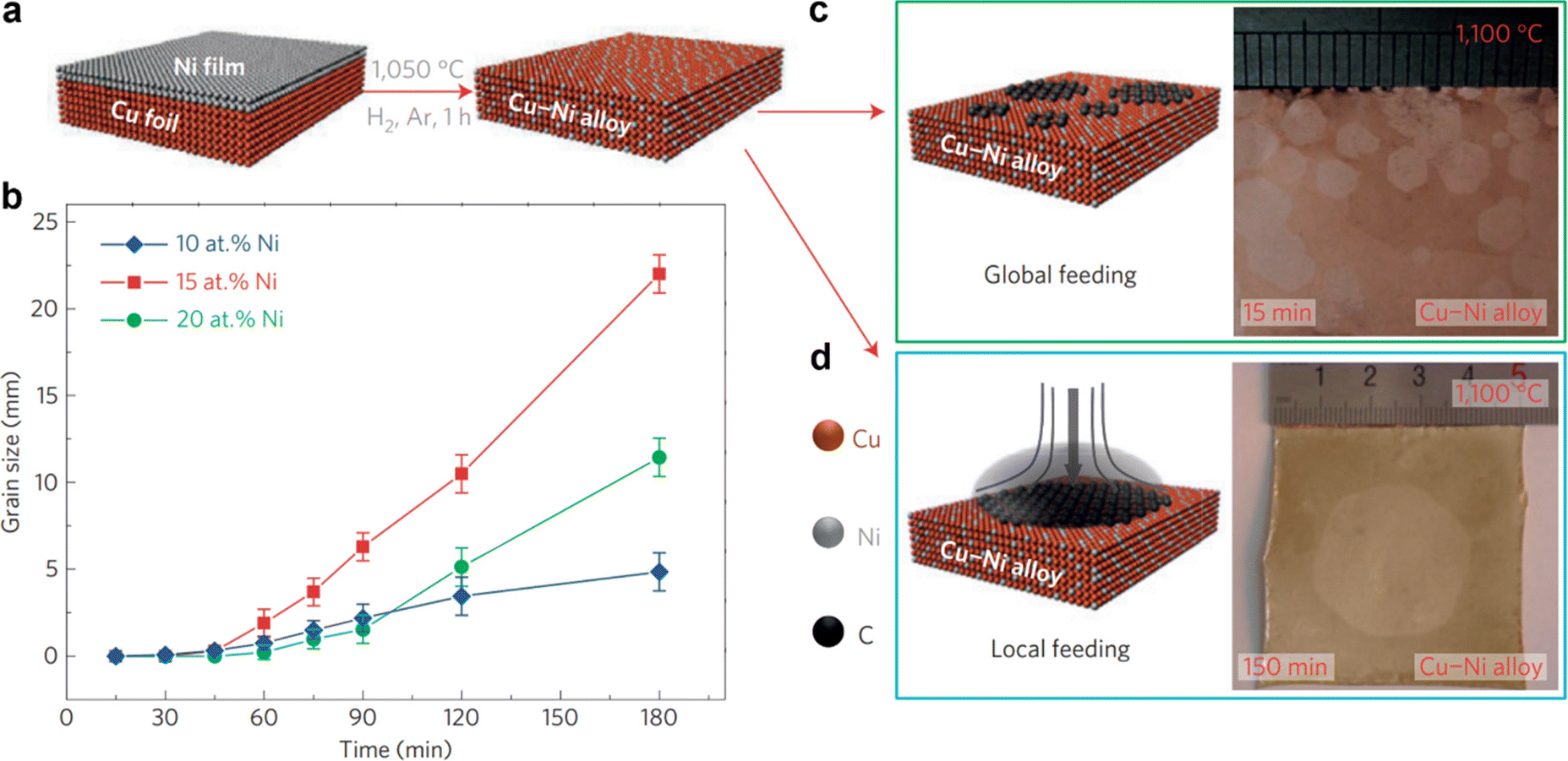 | ||
| Fig. 1 (a) Schematic illustrations of the formation of the Cu–Ni alloy. (b) Comparison of graphene growth rates on different Cu–Ni alloy substrates at the growth temperature. (c) Schematic illustration of the global precursor feeding CVD process (left) and optical microscopy image of multiple nucleation and ultrafast growth of graphene (right) on the Cu85Ni15 alloy. (d) Schematic illustration of the local precursor feeding process (left) and optical microscopic image of a 2-inch size single crystal graphene film grown from a single nucleus (right). [Fig. 1 is reproduced with permission from Wu et al.65 Copyright 2015, rights managed by the Nature Publishing Group]. | ||
Although the nucleation density can be reduced by the above mentioned growth strategies, inevitably, some new nuclei appear during growth, prohibiting the further growth of single-crystal graphene domains larger than the distance between the initial neighboring nuclei. Moreover, many structural defects are also commonly observed in the CVD-grown single-crystal graphene. Ma et al. demonstrated that the edges of graphene, which are the sites at which carbon accumulates in the 2D honeycomb lattice, significantly influence its growth. The growth and etching rate of the single-crystal graphene domain increase linearly with the slanted angle of its edges and are reversible in nature.49 On the basis of this understanding, in a separate work Ma et al. developed a repeated growth–etching–regrowth (G–E–RG) process, to fabricate large-area defect-free single-crystal graphene.91 Where a high CH4 flow rate was applied for 10 min at the initial stage to enable rapid nucleation and growth of graphene domains. Then the flow of CH4 was switched off and pure H2 gas was introduced for 1 min to induce etching of newly formed nuclei, subsequently, H2 gas supply was switched off and growth conditions were reintroduced to grow the desired graphene domains further into a large-area single-crystal.
The Cu (111) surface plane is a more efficient and cheaper alternative to Ge (110) for its low lattice mismatch (∼4%) with the honeycomb lattice of graphene, enabling epitaxially aligned nucleation and growth of graphene domains. For instance, Xu et al. has demonstrated the formation of a 5 × 50 cm2 graphene film with >99% highly oriented grains within 20 minutes on single-crystal Cu (111) foil, facilitated by epitaxial growth of highly aligned graphene islands and their seamless merging (Fig. 2a–d).93Fig. 2a shows Cu (111) foils with ∼60% (top), ∼90% (middle) and 100% (bottom) graphene coverage. Fig. 2b–d shows the Cu (111) foil areas with fully covered graphene, areas with aligned large graphene islands and areas with aligned small graphene islands, respectively.
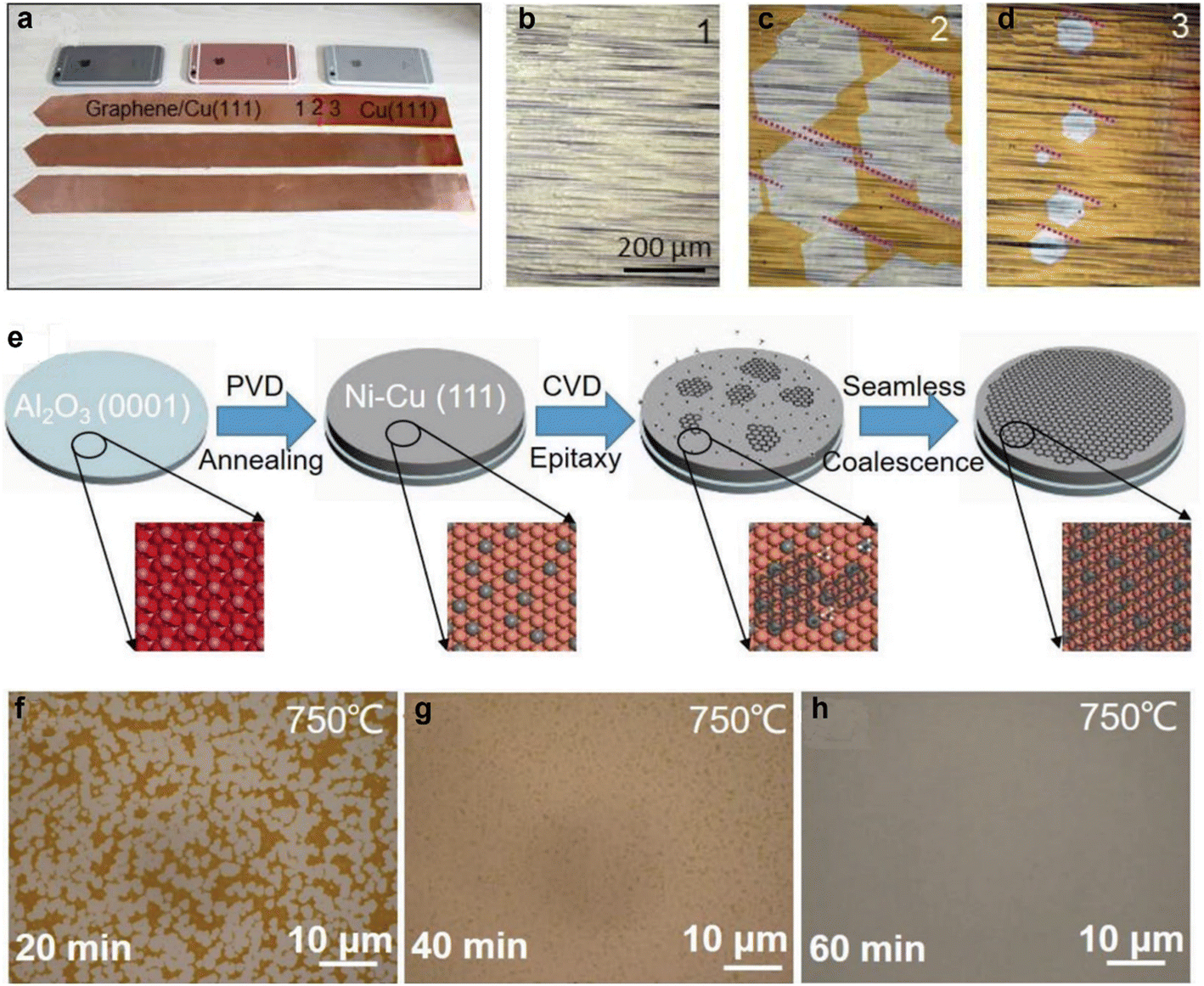 | ||
| Fig. 2 (a) Cu (111) foils with graphene coverages of ∼60% (top panel), ∼90% (middle panel) and 100% (bottom panel), where the “shining” parts are graphene/Cu (left side). Three iPhone 6 devices are placed nearby as a reference. (b–d) Optical images of three regions of the graphene covered Cu (111) foil (marked as 1, 2, 3) in (a). (e) Schematics for the fabrication of wafer-scale single-crystal graphene on the Cu/Ni (111) alloy film at a low temperature. (f–h) Typical optical microscopy (OM) images of the evolution of graphene domains on the Cu/Ni (111) alloy film from individual grains to a continuous single crystal at 750 °C. [Fig. 2(a)–(d) are reproduced with permission from Xu et al. Copyright 2017, Elsevier Publishing Company. Fig. 2(e)–(h) are reproduced with permission from Zhang et al. Copyright 2019, Wiley-VCH, Weinheim]. | ||
The Pt (111) substrate is also of distinctive interest for the growth of high-quality graphene films, due to its similar carbon solubility similar to Cu (111) and relatively higher melting temperature (1768 °C) and lower thermal expansion coefficient than Cu. Therefore, compared to Cu (111), it can reduce the surface atom agglomeration and rough morphology under CVD growth conditions, thereby decreasing the nucleation density and point defects in graphene, and the density of wrinkles during the thermal quenching process.94,95 Using Pt (111) as the growth substrate, Cheng et al. have grown a millimeter-sized defect-free single-crystal graphene film by the ambient-pressure CVD method and transfer these single-crystal graphene films to an arbitrary substrate, by using a nondestructive bubbling transfer method to enable the reuse of the Pt (111) substrate.91,96 Kang et al. has recently reported the CVD growth of 6-inch single-crystal graphene on twinned Pt (111) films. The twinned structure of Pt (111) films does not change the preferential orientation of graphene nuclei, resulting in highly oriented graphene domains on the Pt (111) substrate.97
Huang et al. have recently reported fast growth (in 5 min or less) of large-area single crystal monolayer graphene over “homemade” single crystal Cu/Ni (111) alloy (1.3 at% to 8.6 at% Ni) foils.60 Where the superstructure with Cu6Ni1 at the surface of these Cu/Ni alloy foils allows the epitaxial growth of highly aligned hexagonal graphene islands and their subsequent merger into highly oriented monolayer graphene over the entire substrate. However, this process requires a high growth temperature (1075 °C), which causes metal evaporation and sometimes wrinkles due to the large thermal expansion mismatch between the substrate and graphene during cooling.98 Zhang et al. reported an alternative low temperature (750 °C) method using Cu/Ni (111)/sapphire wafers for epitaxial growth of 6 inch wafer-scale single-crystal graphene film after a 60 min growth (Fig. 2e–h).99Fig. 2e shows the schematic illustration of the two-step growth process and Fig. 2f–h shows the time dependent optical microscopy images of the evolution of graphene domains on the Cu/Ni (111) alloy film at 750 °C. The lower temperature requirement in this process could be due to either lower dehydrogenation energy of the carbon precursor, lower diffusion energy of carbon species on the Cu/Ni (111) alloy film surface, or lower energy barrier for attaching a carbon cluster to the as-formed graphene edge.
In a recent study, Li et al. have combined both the strategies nucleation control and unidirectional alignment of grains to produce wafer-scale single-crystal monolayer graphene on Cu (111)/Al2O3 (0001) wafers using a multi-cycle plasma etching-assisted-chemical vapor deposition (MPE-CVD) growth method (Fig. 3).27Fig. 3a schematically shows the four stages of the synthesis process, where the stage-1 (carbon diffusion), stage-2 (graphene growth) and stage-3 (plasma cleaning) reaction cycle was repeated many times until wafer-scale growth of single-crystal monolayer graphene at the interface between Cu (111) and Al2O3 (0001). Finally at stage-4, the Cu (111) film was bulged and peeled off to get inch-scale single-crystal graphene film directly on the insulating Al2O3 (0001) substrate. Graphene nucleation density at the Cu (111)–Al2O3 (0001) interface was controlled by tuning the graphene coverage (by means of plasma cleaning) on the top surface of Cu (111) and hence the diffusivity of the dissolved carbon atoms in and through Cu (111), which acts as carbon sources for graphene growth at the interface. It was found that the hexagonal shape and sharp edges of aligned graphene islands were formed at the Cu (111)–Al2O3 (0001) interface, which promotes the seamless merging of the graphene islands and produces a single-crystal wafer-scale as-grown graphene film. The effectiveness of this synthesis process relies on the hexagonal symmetry and the best lattice consistency with a minimal lattice mismatch of 6.5% between Cu (111) and Al2O3(0001). Moreover, the stacking energies per Cu atom were 0.98, 1.33 and 2.09 eV for Cu (110), Cu (100) and Cu (111), respectively, indicating that Cu (111) is energetically favorable (Fig. 3b). Fig. 3c schematically shows the dissolution of carbon atoms in Cu (111) and the formation of a Cu–C alloy, which ensures continuous diffusion of carbon atoms to the Cu (111)–Al2O3 (0001) interface. Subsequently, the predominant formation of the graphene layer at the Cu (111)–Al2O3 (0001) interface was determined by the highest carbon binding energies of graphene (0.304 eV per carbon atom) at the Cu (111)–Al2O3 (0001) interface compared to Cu (111, 0.204 per carbon atom) and Al2O3 (0001, 0.200 per carbon atom). In a theoretical paper, Chen et al. discuss the kinetics and energetics of carbon nucleation in the early stages of graphene epitaxial growth on various metal surfaces.100 The major interaction responsible for the preferential nucleation of graphene on various metal surfaces is listed in Table 1.
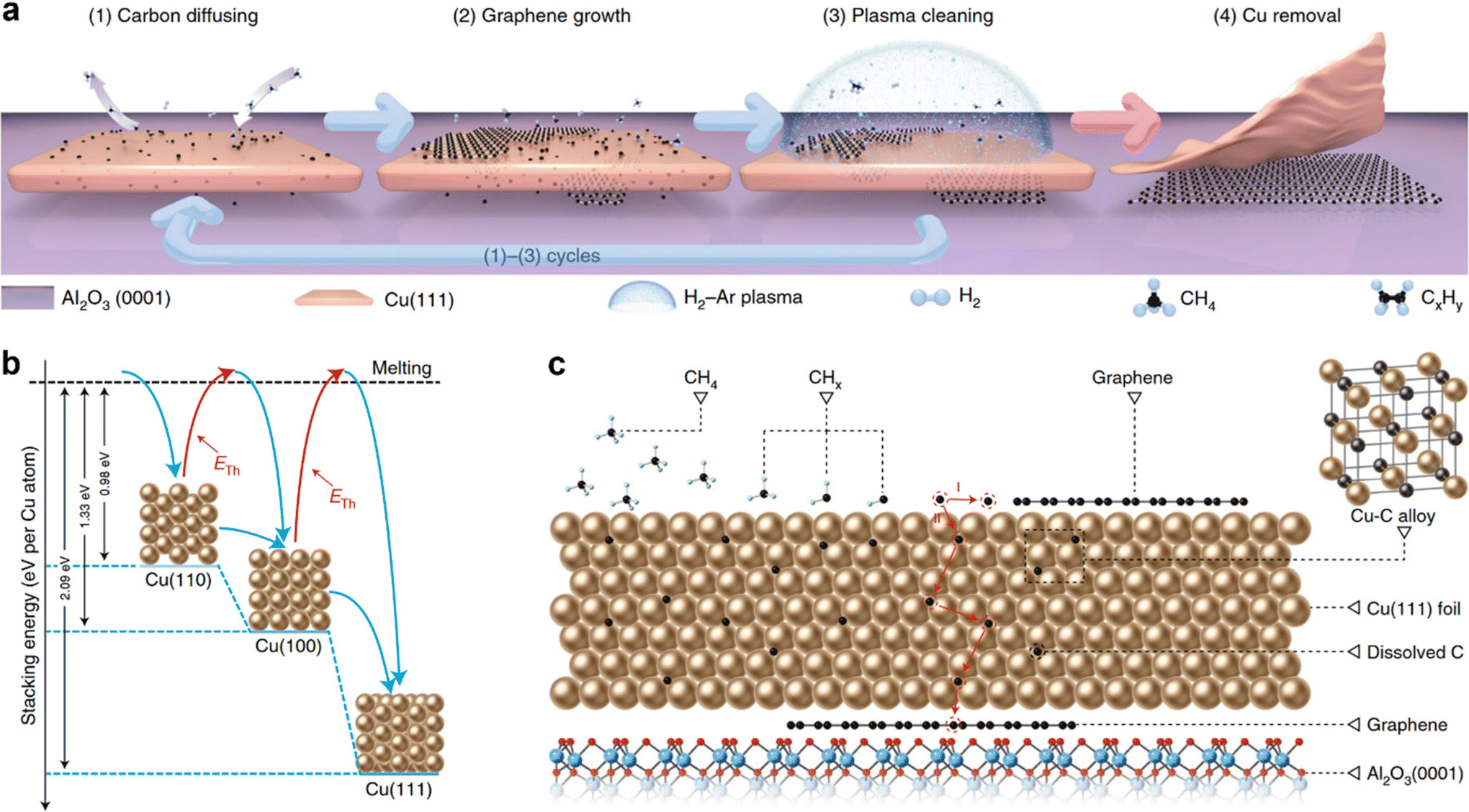 | ||
| Fig. 3 (a) The synthesis scheme of wafer-scale single-crystal monolayer graphene thin film on electrically insulating Al2O3 (0001) wafers by a multi-cycle plasma etching-assisted-chemical vapor deposition (MPE–CVD) method. (b) Stacking energies of Cu (100), Cu (110) and Cu (111) on Al2O3 (0001). (c) Schematic showing the dissolution of carbon atoms in Cu (111) and the formation of a Cu–C alloy, which ensures continuous diffusion of carbon atoms to the Cu (111)–Al2O3 (0001) interface. [Fig. 3 is reproduced with permission from Li et al.27 Copyright 2022, rights managed by the Nature Publishing Group]. | ||
| Metal substrates | Major interactions responsible for preferential nucleation of graphene | Ref. |
|---|---|---|
| Cu (111) and Cu (110) | Strong interaction between the graphene zigzag edge and the Cu 〈110〉 step edge leads to the unidirectional alignment of graphene islands on Cu (111) or Cu (110) substrates | Ref. 101 |
| Ni (111) and Ni (110) | Strong interaction of graphene with the low-index Ni (111) and Ni (110) faces offsets the bending film stresses generated at terrace boundaries or at surface defects | Ref. 102 |
| Pt (111) | Weak coupling of graphene to the Pt (111) substrate, leads to the existence of different rotational alignments and interface structures | Ref. 103 |
| Pd (111) | Formation of Moire’ superstructure patterns by the superposition of honeycomb lattice of graphene and hexagonal lattice of Pd (111) | Ref. 104 |
| Ge (110) | Interaction between anisotropically arranged single-crystal Ge surface and graphene edges is responsible for the orientation determination of graphene seeds during nucleation and early stage of graphene growth | Ref. 26 |
| Ir (111) | Precise epitaxial relation of the 〈110〉C direction of C rows in graphene to the Ir surface dense-packed 〈10![[1 with combining macron]](https://www.rsc.org/images/entities/char_0031_0304.gif) 〉Ir direction is satisfied at high growth temperatures of 1320 K 〉Ir direction is satisfied at high growth temperatures of 1320 K |
Ref. 105 |
| Rh (111) | Bonding to the substrate is delocalized over the molecular π backbone of honeycomb carbon units (7C6 clusters), which essentially bind to the substrate via the peripheral carbon atoms | Ref. 106 |
3.2. Synthesis of a wafer-scale single crystal hBN film
The CVD process is widely used to grow mono- or few-layer hBN on catalytic substrates, including Cu,107–109 Ni,110,111 Pt,112,113 and Ru.114 However, the typical grain size of CVD-grown monolayer hBN films are very small (usually <50 μm2), because of the high nucleation density at the early growth stages, and the three-fold symmetry of the hBN lattice, which leads to antiparallel domains and twin boundaries on most substrates.61,115,116 The small grains lead to high density of grain boundaries and dangling bonds, which are known as structural defects in hBN.117,118 Although micrometer-sized hBN grains have been commonly employed for fundamental studies,119 wafer-scale single-crystal hBN (SC-hBN) films are not yet easily available for practical applications. In this section, we review the recent strategies adopted for the synthesis of wafer-scale single-crystal mono- or few-layer h-BN films.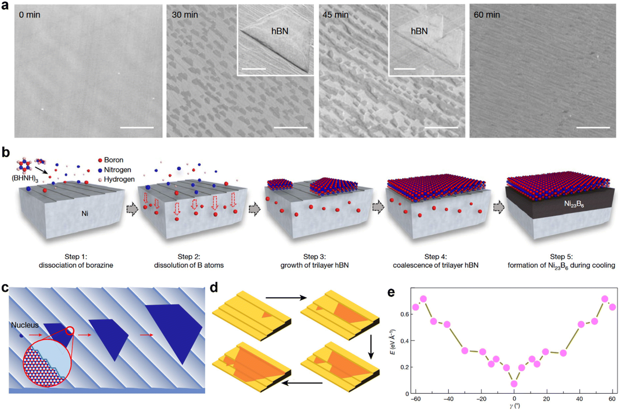 | ||
| Fig. 4 (a) Scanning electron microscopy images showing the time-dependent growth process of trilayer hBN on a Ni (111) foil surface at 1220 °C. The inset show two different high-magnification SEM images, each showing hBN islands. (b) Schematic illustration of the proposed growth pathway of the trilayer hBN film on Ni (111) and the subsequent appearance of Ni23B6 at the Ni (111)/hBN interface. (c) Schematic illustration of hBN nucleation and growth on the Ni (111) surface. (d) Schematic diagrams highlighting the unidirectional growth of hBN domains and the anisotropic growth speed on a Cu surface with steps edges. (e) First-principles calculations of the formation energies of various hBN edges attached to a Cu 〈211〉 step on the Cu (110) substrate at different angle (γ). [Fig. 4(a)–(c) are reproduced with permission from Ma et al.24 Copyright 2022, rights managed by the Nature Publishing Group. Fig. 4(d) and (e) are reproduced with permission from Wang et al.19 Copyright 2019, rights managed by the Nature Publishing Group]. | ||
Although bulk single crystal Cu foil might be suitable for roll-to-roll production of single crystal hBN films, it is not compatible with the current microelectronic device fabrication line on wafers. Chen et al. have recently demonstrated wafer-scale epitaxial growth of single-crystal hBN monolayers on Cu (111) thin film deposited over a two-inch c-plane sapphire wafer (Fig. 5).22 Where the epitaxial growth was facilitated by the lateral docking of hBN to the spontaneously present top-layer Cu (111) step edges, ensuring the mono-orientation of hBN monolayers by breaking the energy degeneracy of rotational twins differing by 60° or 180°. The growth of single-crystal hBN monolayers was carried out by flowing ammonia borane precursors onto the one-inch single-crystal Cu (111) thin film/sapphire in a hot-wall CVD furnace. Fig. 5a shows the optical microscopy (OM) image of monolayer hBN triangular flakes grown on a Cu (111) thin film with 60° in-plane rotated twin grains marked by blue and red dotted triangles. Whereas Fig. 5b shows the OM image of unidirectionally aligned monolayer hBN triangular flakes grown on a Cu (111) thin film, therefore, eliminating the possibility that twin hBN grain formation on Cu (111) is the critical factor to ensure the growth of single crystal hBN on the Cu (111) surface. Density functional theory (DFT) calculations were employed to investigate the epitaxy of the hBN seed (B6N7) at nucleation, with and without considering Cu (111) step-edge docking (Fig. 5c and d). Fig. 5c shows the lowest-energy atomic arrangements of six B6N7-Cu (111) units, considering the edge docking to two opposite step-edge terminations (A and B) of top-layer Cu (111). Where the B6N7 seeds are restricted to 0° (or 60°) orientation when docking to A (or B) steps. Based on the calculated binding energies of the six B6N7-Cu (111) configurations, B6N7 seeds should kinetically nucleate while docking to stronger binding sites, B types (edge-to-step), with suitable orientation, to ensure mono-orientated growth (Fig. 5d).
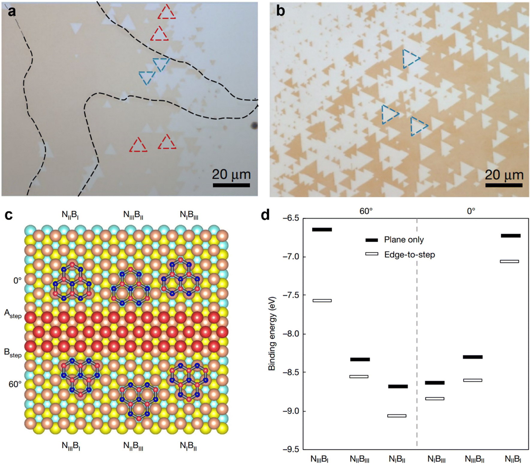 | ||
| Fig. 5 (a) OM image of monolayer hBN triangular flakes grown on a Cu (111) thin film with 60° in-plane rotated twin grains marked by blue and red dotted triangles. (b) OM image of unidirectionally aligned monolayer hBN triangular flakes grown on a Cu (111) thin film. (c) The lowest-energy atomic arrangements of six B6N7-Cu (111) units, considering the edge docking to two opposite step-edge terminations (A and B) of top-layer Cu (111). (d) Calculated binding energies for the six B6N7-Cu (111) configurations, with and without including the edge-to-step epitaxy effect. [Fig. (a–d) are reproduced with permission from Chen et al.22 Copyright 2020, rights managed by the Nature Publishing Group]. | ||
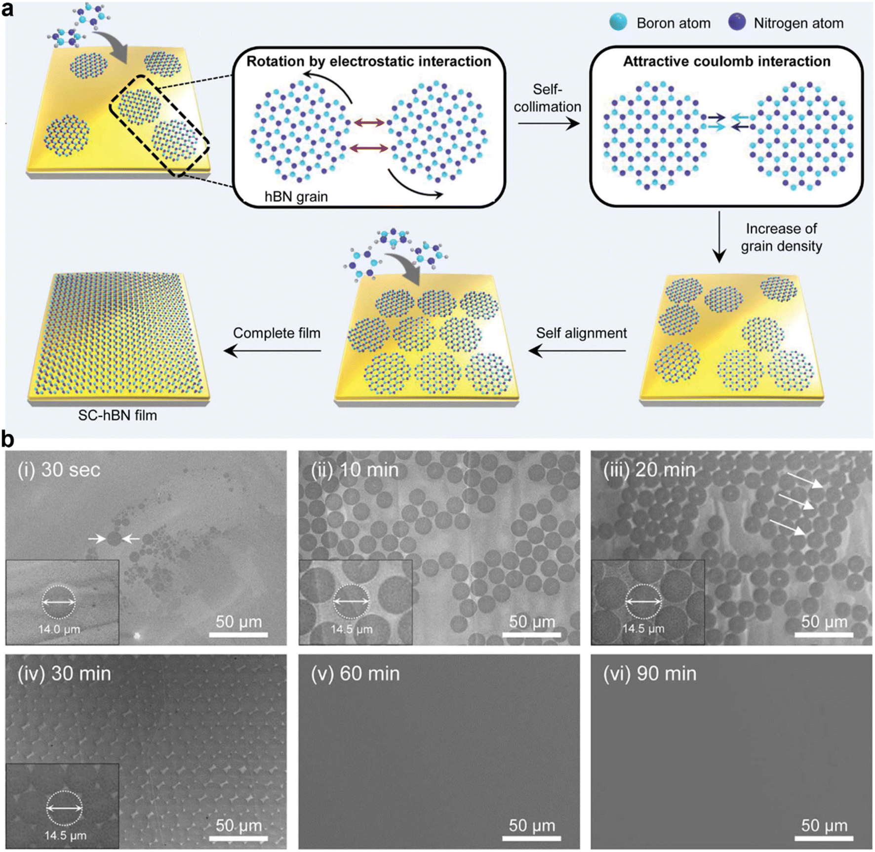 | ||
| Fig. 6 (a) Schematic illustration of the synthesis of the wafer-scale single crystal hexagonal boron nitride (hBN) film via self-collimation of randomly oriented grains on a liquid Au surface. (b) Scanning electron microscopy images of the hBN thin film growth process at different growth times. [Fig. 6 is reproduced with permission from Lee et al.20 Copyright 2018, American Association for the Advancement of Science]. | ||
3.3. Synthesis of wafer-scale single crystal metal chalcogenide (MC) films
Since the metal atoms are passivated by chalcogens at the edges of MCs, their edge formation energies are usually smaller than that of graphene and hBN. Therefore, the energy barrier for stable nuclei formation is smaller, making the process of controlling the nucleation density a challenging task. Experiments have also shown that it is very challenging to realize a very low nucleation density or only one nucleus over a large area.121–123 In contrast, the multi-nucleation approach relies on a lattice-matched substrate, which enables the epitaxial MC domains to grow in the same orientation and then coalesce into a wafer-scale single crystal MC film.93 In this section, we review the state-of-the-art strategies such as unidirectional seeding and nucleation at the vicinal step edges, epitaxial collimation, and seeded in-plane 2D-epitaxy, adopted to induce uniform domain orientation for the synthesis of wafer-scale single crystal MC films.0〉 direction (A axis), the step edges become perpendicular to the zigzag (ZZ) edge of the triangular MoS2 domains, which equalizes the two antiparallel domains and prevents the growth of single crystals. Whereas, as shown in Fig. 7b, when the surface step edges are projected along the 〈100〉 direction (M axis), the degeneracy of nucleation energy for antiparallel MoS2 rotational twin domains are lifted, which leads to unidirectional alignment of the MoS2 domains over the 2-inch wafer-scale. Fig. 7c shows the epitaxial relationship of MoS2 on a sapphire (0001) substrate, where black and red arrows indicate the lattice vectors of the sapphire and MoS2, respectively. Wang et al. have also recently demonstrated the epitaxial growth of 2-inch single-crystal WS2 monolayer films on vicinal a-plane sapphire surfaces (Fig. 7d–i).29Fig. 7d and e shows the schematic of the configuration of the WS2 cluster on a flat a-plane sapphire surface for θ = 0° (Fig. 7d) and 60° (Fig. 7e), where θ is the angle between one zigzag direction of WS2 and the 〈100〉 plane of the a-plane sapphire surface. Top panel of Fig. 7f, shows the binding energy of WS2 triangular islands with the a-plane sapphire surface at different rotational angles. Where the binding energy minima reflecting the configurations are shown in Fig. 7d and e. Bottom panel of Fig. 7f, shows the relative energy difference between the antiparallel WS2 islands upon interaction and cross-over of the step-edges in the a-plane sapphire surface due to symmetry breaking. Fig. 7g and h show the calculated distributions of charge difference of the antiparallel (θ = 0° and 60°) WS2 islands at the step-edges of a-plane sapphire. This indicates that the binding energy between the step edge and WS2 depends on its alignment and breaks the C2 symmetry of the WS2/a-plane sapphire system into C1, making it possible to have all the WS2 islands aligned only along one direction, leading to the formation of wafer-scale single crystal upon coalescence (Fig. 7i).
 | ||
| Fig. 7 (a and b) Surface step edge orientation along the 〈110〉 direction (A axis) and along the 〈100〉 direction (M axis) of sapphire (0001), respectively, and the corresponding epitaxial MoS2 domain alignment. (c) The epitaxial relationship of MoS2 on a sapphire (0001) substrate. Black and red arrows indicate the lattice vectors of the sapphire and MoS2, respectively. Schematic of the configuration of the WS2 cluster on a flat a-plane sapphire surface for θ = 0° (d) and 60° (e), where θ is the angle between one zigzag direction of WS2 and the 〈100〉 plane of the a-plane sapphire surface. (f) Binding energy of WS2 triangular islands with a-plane sapphire surface at different rotational angles (top panel). Relative energy difference between the antiparallel WS2 islands upon interaction and cross-over of the step-edges in a-plane sapphire (bottom panel). (g and h) Calculated distributions of charge difference of the antiparallel (θ = 0°, (g) and 60°, (h) WS2 islands at the step-edges of a-plane sapphire. (i) Schematic of WS2 islands grown on a-Al2O3 during the early stage of growth. [Fig. 7(a)–(c) are reproduced from Li et al.28 Copyright 2021, rights managed by the Nature Publishing Group. Fig. 7(d)–(i) are reproduced from Wang et al.29 Copyright 2021, rights managed by the Nature Publishing Group]. | ||
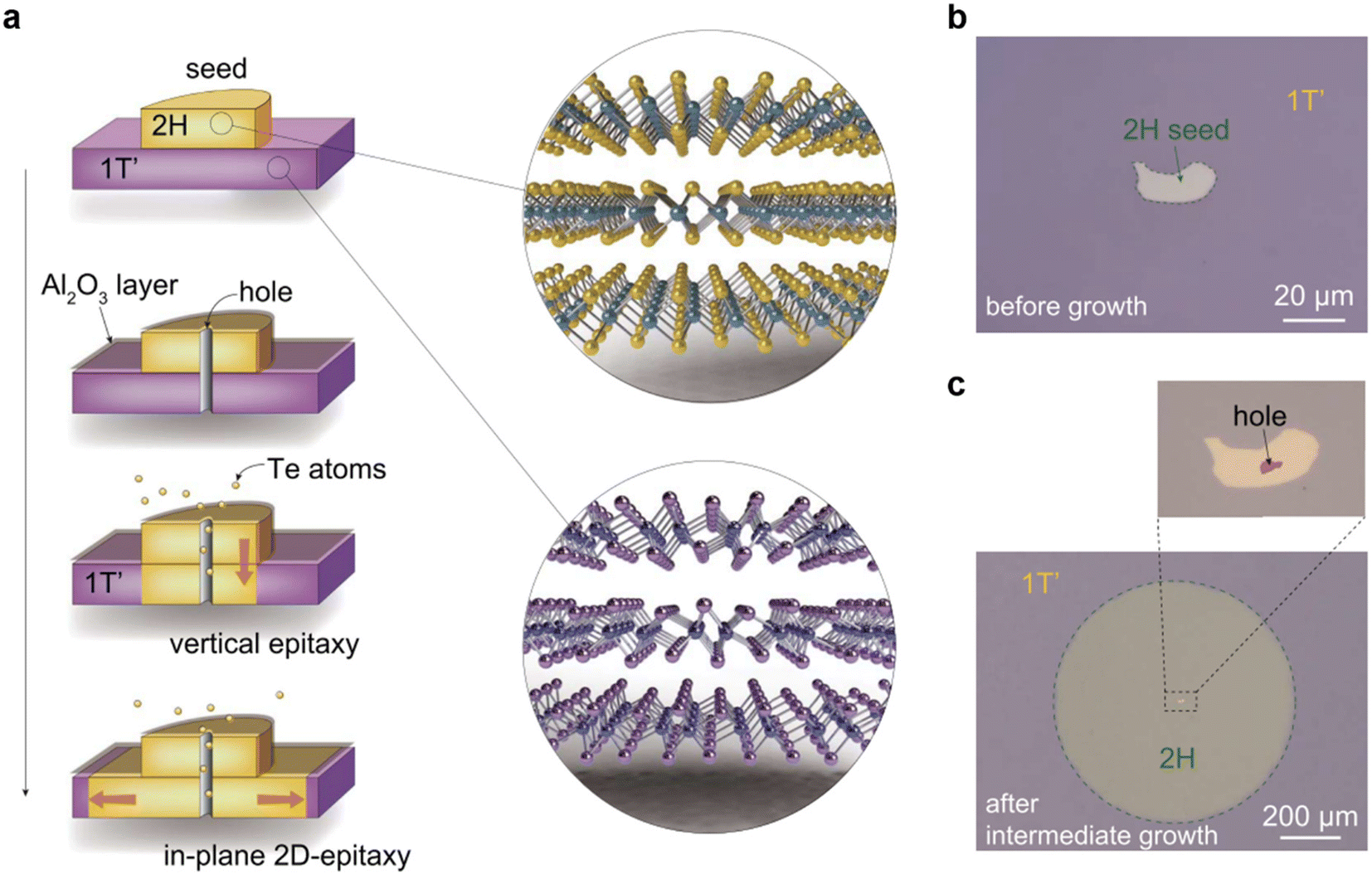 | ||
| Fig. 8 (a) Schematic illustration showing the in-plane 2D-epitaxy mediated synthesis of a wafer-scale single-crystal 2H-MoTe2 thin film. The 1T′-MoTe2 film on a Si wafer was converted gradually via phase transition and recrystallization to the 2H-MoTe2, starting from the hole to the entire area. (b) OM image of a 2H MoTe2 nanoflake assembled in the center of the 1T′ MoTe2 wafer as a seed to induce the phase transition and recrystallization. (c) OM image of the wafer after intermediate growth at 650 °C for 2 hours, where the seed crystal with a needle probe-punched hole is shown in the inset. [Fig. 8 is reproduced with permission from Xu et al.130 Copyright 2021, American Association for the Advancement of Science]. | ||
Since 1T′ MoTe2 is Te deficient, Te atoms were supplied through a hole on 30 nm-thick Al2O3 covered 2H MoTe2 flake, to avoid any direct contact between Te and 1T′ MoTe2. This site-specific Te supply pathway induces the 1T′ to 2H MoTe2 phase transition exactly underneath the 2H MoTe2 seed crystal,131–133 and simultaneously avoids the spontaneous nucleation of 2H MoTe2 with random crystal orientations in the 1T′ MoTe2 film. With the continuous supply of Te, through the outward transmission of phase transition and recrystallization induced by the vertical 2H/1T′ interface, eventually the 1T′ MoTe2 layer underneath the seed crystal transformed into a wafer-scale 2H MoTe2 single crystal with the same crystallographic orientation as the seed crystal. Fig. 8b shows the OM image of the 2H/1T′ MoTe2 assembly, where a 2H MoTe2 seed nanoflake is placed at the center of the 1T′ MoTe2 wafer. Fig. 8c shows the OM image of the 1T′ MoTe2 wafer at an intermediate growth stage, resulting in a single crystal 2H MoTe2 circle centered on the seed region. The inset shows the seed crystal with a needle probe-punched hole.
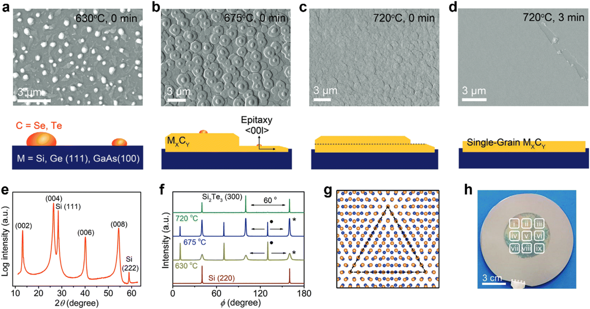 | ||
| Fig. 9 (a–d) Field emission scanning electron microscopy (FE-SEM) images of the Si2Te3 thin film growth process at different temperatures. (e) XRD pattern of the Si2Te3 film exhibited only [00l] out-of-plane orientation. (f) Azimuthal φ-scan of the in-plane (300) reflection of Si2Te3 at different annealing temperatures. The peak in perfect epitaxial alignment with the Si (220) is indicated by “*” and the peak having 30° mismatch with Si (220) is indicated with “•”. (g) The coincidence site lattice (CSL) (dotted triangle) in the interface model between the Te (yellow) layer of Si2Te3 and Si (blue) of Si (111). (h) Digital image of 2-inch single-grain Si2Te3 thin film grown on the 4-inch Si (111) wafer. [Fig. 9 is adopted with permission from Giri et al.21 Copyright 2021, Wiley-VCH, Weinheim]. | ||
4. Conclusion and outlook
The novel properties4,134,135 and promising applications4,136–138 of 2D vdW materials have motivated increasing attempts to synthesize high quality 2D vdW thin films since monolayer graphene was prepared.139–141 To realize their industrial applications, which is the ultimate goal, it is of paramount importance to have readily available wafer-scale single crystal thin films of 2D vdW materials.14,15 Although the nucleation-controlled growth by suppressing the nucleation density is an effective strategy to produce large-scale single crystal graphene,65 due to its lower growth rate it takes several hours to grow a fully covered wafer-scale graphene film. Nevertheless, because of the complicated experimental design and the sensitivity of the process to control gas flow in the reactor, the process is not cost-effective and inconvenient. In contrast, unidirectional alignment of multiple epitaxial nuclei and their seamless coalescence into a large-area single crystal graphene, have several advantages including shorter growth time and require lesser stringent growth conditions.74 Recent successful growth of wafer-scale single crystal graphene monolayers directly on electrically insulating Al2O3 (0001) wafers could also contribute to next-generation graphene-based nanodevices.27Recent studies have shown the growth of single crystal hBN films on molten gold surfaces or bulk Cu or Ni foils.19,20,24 However, the use of molten gold is not favored by industry, owing to its high cost, cross-contamination and potential issues of process control and scalability. Copper foils might be suitable for roll-to-roll processes but are unlikely to be compatible with advanced microelectronic fabrication on wafers. However, the successful epitaxial growth of 2-inch single-crystal hBN monolayers on a Cu (111) thin film deposited over c-plane sapphire wafer is a reliable approach to produce wafer-scale single-crystal hBN and paves the way to future 2D electronics.22 More studies are needed on the synthesis of multilayer hBN on low-symmetry single crystalline substrates in the future.
The recent successful synthesis of wafer-scale single crystal MoS2 and WS2 monolayers on Al2O3 surfaces with periodic step-edges boosted research interest in synthesizing wafer-scale 2D vdW MC thin films where the microstructure and unidirectional nature of the monolayer are attributed to the high nucleation density along the sapphire surface steps and their seamless coalescence of the aligned domains. However, the production of the well-aligned step-edges is technologically very challenging to reproduce.28,29,32 Moreover, upon high-temperature (>850 °C) exposure, the step-edges tend to distort, resulting in the nucleation of MC domains in various orientations.127 Growth conditions that preserve the aligned step-edge morphology while promoting surface diffusion and lateral domain growth are necessary to reduce domain mis-orientation and achieve unidirectional growth. In this regard, the generalized epitaxial synthetic concept, viz. “surface diffusion and epitaxial self-planarization”, for the production of wafer-scale single crystal metal chalcogenide thin films (Si2Te3, GeTe, GeSe, and GaTe) directly on commercial wafers (Si, Ge, GaAs, etc.) and their utilization in the transfer-free fabrication of devices, is believed to open a new technological window for both the 2D vdW wafer-scale single crystal synthesis and the device fabrication process.21 Although the continuous epitaxial films resulting from the coalescence of orientationally aligned islands have essentially one crystallographic orientation, translational grain boundaries along high-symmetry directions still exist because of the presence of imperfectly coalesced domains.127,128 Such regions of coalescence sometimes can be located by arrays of metal vacancies in the MC monolayer, leaving behind arrays of point defects.129 A recently developed method of seeded 2D epitaxial growth of a wafer-scale single crystal film of semiconducting 2H MoTe2via solid-to-solid phase transition and recrystallization processes, mitigates this issue of imperfect coalescence,130 which can be used as a template for further rapid epitaxy in a vertical manner.
Although recently several epitaxial growth strategies of wafer-scale 2D vdW single-crystal films have been demonstrated, the industrial scale production of 2D materials is still a big challenge, especially compared to chip-grade single-crystal silicon. One problem is how to grow single crystal 2D vdW materials with high uniformity and excellent electrical properties on a wafer scale. Currently, the main method of growing single crystal thin films is to control the unidirectional orientation of the crystal domains to allow their seamless coalescence and stitching. However, the continuous epitaxial films resulting from the coalescence of orientationally aligned islands are also expected to exhibit facets along high-symmetry directions.128 Moreover, translational defect arrays and grain boundaries still exist in a nearly single-orientation, coalesced monolayer 2D vdW film due to the presence of imperfectly stitched domains.127–129 These defective grain boundaries in 2D semiconductors usually exhibit metallic characteristics and serve as conducting channels, seriously impairing the electrical and optical properties of related devices. Therefore, connecting atomic-scale defects to larger morphologies poses a significant challenge. Additionally, it has been difficult to control the nucleation of 2D materials to get a unidirectionally aligned multilayer single-crystal 2D vdW film on the wafer scale. The indefinite kinetic control of the layer-by-layer growth of 2D vdW materials arises due to the complexity of the precursor species and their gradient feeding distributions along the gas flow direction. Also, currently the synthesized 2D vdW thin films need to be transferred from the growth substrate to the target substrate for device fabrication. However, the traditional transfer process can damage the grown films, due to the formation of wrinkles, cracks, and polymer contamination, seriously affecting the device performance of the synthesized 2D vdW thin films.
Finally, the technique for the mass production of wafer-scale single crystal 2D vdW materials must be able to provide the required quantities while ensuring reliable quality for industrial-scale applications. The development of a reliable large-scale production process, with special emphasis on quality, cost, reproducibility, processability and safety, would not only unleash the potential of 2D vdW materials in electronic and optoelectronic applications, but may also help trigger other key applications, where the unique properties of 2D vdW materials can produce significant enhancements. However, the growth model of 2D vdW materials is far from complete and further attention and efforts are required, including increasing precursor supply, local feeding of precursors, and reduction of pre-deposited transition metal containing thin films, to elucidate the growth mechanism of wafer-scale single crystal 2D vdW materials.
Conflicts of interest
There are no conflicts to declare.Acknowledgements
The authors thank SERB, India (Grant No. CRG/2019/000896, SRG/2021/001184 and P-07/749) and IOE, India (Scheme No.: 6031 and Seed Grant-II/2021-22/39994) for financial support to carry out this research. C. G. thanks UGC for fellowship. A. G. thanks SERB India (Project No. CRG/2022/000960) for financial support.References
- K. S. Novoselov, A. Mishchenko, A. Carvalho and A. H. Castro Neto, Science, 2016, 353, aac9439 CrossRef CAS PubMed.
- K. F. Mak, C. Lee, J. Hone, J. Shan and T. F. Heinz, Phys. Rev. Lett., 2010, 105, 136805 CrossRef PubMed.
- M. Xu, T. Liang, M. Shi and H. Chen, Chem. Rev., 2013, 113, 3766–3798 CrossRef CAS PubMed.
- A. Giri, G. Park and U. Jeong, Chem. Rev., 2023, 123, 3329–3442 CrossRef CAS PubMed.
- M. C. Lemme, D. Akinwande, C. Huyghebaert and C. Stampfer, Nat. Commun., 2022, 13, 1392 CrossRef CAS PubMed.
- M. Zeng, Y. Xiao, J. Liu, K. Yang and L. Fu, Chem. Rev., 2018, 118, 6236–6296 CrossRef CAS PubMed.
- F. Xia, H. Wang, D. Xiao, M. Dubey and A. Ramasubramaniam, Nat. Photonics, 2014, 8, 899–907 CrossRef CAS.
- W. Miao, L. Wang, X. Mu and J. Wang, J. Mater. Chem. C, 2021, 9, 13600–13616 RSC.
- L. J. Li, E. C. T. O'Farrell, K. P. Loh, G. Eda, B. Özyilmaz and A. H. Castro Neto, Nature, 2016, 529, 185–189 CrossRef CAS PubMed.
- C. Tőke and V. I. Fal'ko, Phys. Rev. B: Condens. Matter Mater. Phys., 2014, 90, 035404 CrossRef.
- J. T. Ye, Y. J. Zhang, R. Akashi, M. S. Bahramy, R. Arita and Y. Iwasa, Science, 2012, 338, 1193–1196 CrossRef CAS PubMed.
- J. M. Park, Y. Cao, L.-Q. Xia, S. Sun, K. Watanabe, T. Taniguchi and P. Jarillo-Herrero, Nat. Mater., 2022, 21, 877–883 CrossRef CAS PubMed.
- Y. Cao, V. Fatemi, S. Fang, K. Watanabe, T. Taniguchi, E. Kaxiras and P. Jarillo-Herrero, Nature, 2018, 556, 43–50 CrossRef CAS PubMed.
- D. Neumaier, S. Pindl and M. C. Lemme, Nat. Mater., 2019, 18, 525–529 CrossRef CAS PubMed.
- V. Dusastre, Nat. Mater., 2019, 18, 519–519 CrossRef PubMed.
- L. Lin, H. Peng and Z. Liu, Nat. Mater., 2019, 18, 520–524 CrossRef CAS PubMed.
- A. K. Singh, B. Thakurta, A. Giri and M. Pal, Chem. Commun., 2024, 60, 265–279 RSC.
- J. Zhou, J. Lin, X. Huang, Y. Zhou, Y. Chen, J. Xia, H. Wang, Y. Xie, H. Yu, J. Lei, D. Wu, F. Liu, Q. Fu, Q. Zeng, C.-H. Hsu, C. Yang, L. Lu, T. Yu, Z. Shen, H. Lin, B. I. Yakobson, Q. Liu, K. Suenaga, G. Liu and Z. Liu, Nature, 2018, 556, 355–359 CrossRef CAS PubMed.
- L. Wang, X. Xu, L. Zhang, R. Qiao, M. Wu, Z. Wang, S. Zhang, J. Liang, Z. Zhang, Z. Zhang, W. Chen, X. Xie, J. Zong, Y. Shan, Y. Guo, M. Willinger, H. Wu, Q. Li, W. Wang, P. Gao, S. Wu, Y. Zhang, Y. Jiang, D. Yu, E. Wang, X. Bai, Z.-J. Wang, F. Ding and K. Liu, Nature, 2019, 570, 91–95 CrossRef CAS PubMed.
- J. S. Lee, S. H. Choi, S. J. Yun, Y. I. Kim, S. Boandoh, J.-H. Park, B. G. Shin, H. Ko, S. H. Lee, Y.-M. Kim, Y. H. Lee, K. K. Kim and S. M. Kim, Science, 2018, 362, 817–821 CrossRef CAS PubMed.
- A. Giri, M. Kumar, J. Kim, M. Pal, W. Banerjee, R. D. Nikam, J. Kwak, M. Kong, S. H. Kim, K. Thiyagarajan, G. Kim, H. Hwang, H. H. Lee, D. Lee and U. Jeong, Adv. Mater., 2021, 33, 2102252 CrossRef CAS PubMed.
- T.-A. Chen, C.-P. Chuu, C.-C. Tseng, C.-K. Wen, H. S. P. Wong, S. Pan, R. Li, T.-A. Chao, W.-C. Chueh, Y. Zhang, Q. Fu, B. I. Yakobson, W.-H. Chang and L.-J. Li, Nature, 2020, 579, 219–223 CrossRef CAS PubMed.
- D. Luo, M. Wang, Y. Li, C. Kim, K. M. Yu, Y. Kim, H. Han, M. Biswal, M. Huang, Y. Kwon, M. Goo, D. C. Camacho-Mojica, H. Shi, W. J. Yoo, M. S. Altman, H.-J. Shin and R. S. Ruoff, Adv. Mater., 2019, 31, 1903615 CrossRef PubMed.
- K. Y. Ma, L. Zhang, S. Jin, Y. Wang, S. I. Yoon, H. Hwang, J. Oh, D. S. Jeong, M. Wang, S. Chatterjee, G. Kim, A. R. Jang, J. Yang, S. Ryu, H. Y. Jeong, R. S. Ruoff, M. Chhowalla, F. Ding and H. S. Shin, Nature, 2022, 606, 88–93 CrossRef CAS PubMed.
- M. Wang, M. Huang, D. Luo, Y. Li, M. Choe, W. K. Seong, M. Kim, S. Jin, M. Wang, S. Chatterjee, Y. Kwon, Z. Lee and R. S. Ruoff, Nature, 2021, 596, 519–524 CrossRef CAS PubMed.
- J.-H. Lee, E. K. Lee, W.-J. Joo, Y. Jang, B.-S. Kim, J. Y. Lim, S.-H. Choi, S. J. Ahn, J. R. Ahn, M.-H. Park, C.-W. Yang, B. L. Choi, S.-W. Hwang and D. Whang, Science, 2014, 344, 286–289 CrossRef CAS PubMed.
- J. Li, M. Chen, A. Samad, H. Dong, A. Ray, J. Zhang, X. Jiang, U. Schwingenschlögl, J. Domke, C. Chen, Y. Han, T. Fritz, R. S. Ruoff, B. Tian and X. Zhang, Nat. Mater., 2022, 21, 740–747 CrossRef CAS PubMed.
- T. Li, W. Guo, L. Ma, W. Li, Z. Yu, Z. Han, S. Gao, L. Liu, D. Fan, Z. Wang, Y. Yang, W. Lin, Z. Luo, X. Chen, N. Dai, X. Tu, D. Pan, Y. Yao, P. Wang, Y. Nie, J. Wang, Y. Shi and X. Wang, Nat. Nanotechnol., 2021, 16, 1201–1207 CrossRef CAS PubMed.
- J. Wang, X. Xu, T. Cheng, L. Gu, R. Qiao, Z. Liang, D. Ding, H. Hong, P. Zheng, Z. Zhang, Z. Zhang, S. Zhang, G. Cui, C. Chang, C. Huang, J. Qi, J. Liang, C. Liu, Y. Zuo, G. Xue, X. Fang, J. Tian, M. Wu, Y. Guo, Z. Yao, Q. Jiao, L. Liu, P. Gao, Q. Li, R. Yang, G. Zhang, Z. Tang, D. Yu, E. Wang, J. Lu, Y. Zhao, S. Wu, F. Ding and K. Liu, Nat. Nanotechnol., 2022, 17, 33–38 CrossRef CAS PubMed.
- A. Aljarb, J.-H. Fu, C.-C. Hsu, C.-P. Chuu, Y. Wan, M. Hakami, D. R. Naphade, E. Yengel, C.-J. Lee, S. Brems, T.-A. Chen, M.-Y. Li, S.-H. Bae, W.-T. Hsu, Z. Cao, R. Albaridy, S. Lopatin, W.-H. Chang, T. D. Anthopoulos, J. Kim, L.-J. Li and V. Tung, Nat. Mater., 2020, 19, 1300–1306 CrossRef CAS PubMed.
- S. H. Choi, H.-J. Kim, B. Song, Y. I. Kim, G. Han, H. T. T. Nguyen, H. Ko, S. Boandoh, J. H. Choi, C. S. Oh, H. J. Cho, J. W. Jin, Y. S. Won, B. H. Lee, S. J. Yun, B. G. Shin, H. Y. Jeong, Y.-M. Kim, Y.-K. Han, Y. H. Lee, S. M. Kim and K. K. Kim, Adv. Mater., 2021, 33, 2006601 CrossRef CAS PubMed.
- P. Yang, S. Zhang, S. Pan, B. Tang, Y. Liang, X. Zhao, Z. Zhang, J. Shi, Y. Huan, Y. Shi, S. J. Pennycook, Z. Ren, G. Zhang, Q. Chen, X. Zou, Z. Liu and Y. Zhang, ACS Nano, 2020, 14, 5036–5045 CrossRef CAS PubMed.
- Z. Sun, Z. Yan, J. Yao, E. Beitler, Y. Zhu and J. M. Tour, Nature, 2010, 468, 549–552 CrossRef CAS PubMed.
- X. Yang, Z. Guan, M. Zeng, J. Wei, W. Wang and X. Bai, Small, 2013, 9, 1353–1358 CrossRef CAS PubMed.
- K.-K. Liu, W. Zhang, Y.-H. Lee, Y.-C. Lin, M.-T. Chang, C.-Y. Su, C.-S. Chang, H. Li, Y. Shi, H. Zhang, C.-S. Lai and L.-J. Li, Nano Lett., 2012, 12, 1538–1544 CrossRef CAS PubMed.
- M. J. Allen, V. C. Tung and R. B. Kaner, Chem. Rev., 2010, 110, 132–145 CrossRef CAS PubMed.
- K. S. Novoselov, V. I. Fal′ko, L. Colombo, P. R. Gellert, M. G. Schwab and K. Kim, Nature, 2012, 490, 192–200 CrossRef CAS PubMed.
- L. Zhang, J. Dong and F. Ding, Chem. Rev., 2021, 121, 6321–6372 CrossRef CAS PubMed.
- A. Giri, G. Park, H. Yang, M. Pal, J. Kwak and U. Jeong, Adv. Mater., 2018, 30, 1707577 CrossRef PubMed.
- G. H. Han, D. L. Duong, D. H. Keum, S. J. Yun and Y. H. Lee, Chem. Rev., 2018, 118, 6297–6336 CrossRef CAS PubMed.
- Z. Cai, B. Liu, X. Zou and H.-M. Cheng, Chem. Rev., 2018, 118, 6091–6133 CrossRef CAS PubMed.
- H. Lin, Z. Zhang, H. Zhang, K.-T. Lin, X. Wen, Y. Liang, Y. Fu, A. K. T. Lau, T. Ma, C.-W. Qiu and B. Jia, Chem. Rev., 2022, 122, 15204–15355 CrossRef CAS PubMed.
- C. Dai, Y. Liu and D. Wei, Chem. Rev., 2022, 122, 10319–10392 CrossRef CAS PubMed.
- D. Steiner, M. Thaler, T. Mairegger, F. Mittendorfer and E. Bertel, J. Phys. Chem. C, 2023, 127, 11559–11569 CrossRef CAS.
- M. S. Islam, A. A. M. Mazumder, M. U. Sohag, M. M. H. Sarkar, C. Stampfl and J. Park, Nanoscale Adv., 2023, 5, 4041–4064 RSC.
- Y. Liu, A. Dobrinsky and B. I. Yakobson, Phys. Rev. Lett., 2010, 105, 235502 CrossRef PubMed.
- V. I. Artyukhov, Y. Liu and B. I. Yakobson, Proc. Natl. Acad. Sci. U. S. A., 2012, 109, 15136–15140 CrossRef CAS PubMed.
- H. Shu, X. Chen, X. Tao and F. Ding, ACS Nano, 2012, 6, 3243–3250 CrossRef CAS PubMed.
- T. Ma, W. Ren, X. Zhang, Z. Liu, Y. Gao, L.-C. Yin, X.-L. Ma, F. Ding and H.-M. Cheng, Proc. Natl. Acad. Sci. U. S. A., 2013, 110, 20386–20391 CrossRef CAS PubMed.
- X. Li, J. Dong, J. C. Idrobo, A. A. Puretzky, C. M. Rouleau, D. B. Geohegan, F. Ding and K. Xiao, J. Am. Chem. Soc., 2017, 139, 482–491 CrossRef CAS PubMed.
- Z. Zhang, Y. Liu, Y. Yang and B. I. Yakobson, Nano Lett., 2016, 16, 1398–1403 CrossRef CAS PubMed.
- T. Zhao, J. Guo, T. Li, Z. Wang, M. Peng, F. Zhong, Y. Chen, Y. Yu, T. Xu, R. Xie, P. Gao, X. Wang and W. Hu, Chem. Soc. Rev., 2023, 52, 1650–1671 RSC.
- G. Kim, D. Kim, Y. Choi, A. Ghorai, G. Park and U. Jeong, Adv. Mater., 2023, 35, 2203373 CrossRef CAS PubMed.
- J. Singh, N. A. Astarini, M.-L. Tsai, M. Venkatesan, C.-C. Kuo, C.-S. Yang and H.-W. Yen, Adv. Sci., 2024, 2307839 CrossRef PubMed , n/a.
- J. Gao, J. Zhao and F. Ding, J. Am. Chem. Soc., 2012, 134, 6204–6209 CrossRef CAS PubMed.
- J. Gao, J. Yip, J. Zhao, B. I. Yakobson and F. Ding, J. Am. Chem. Soc., 2011, 133, 5009–5015 CrossRef CAS PubMed.
- A. T. Murdock, A. Koos, T. B. Britton, L. Houben, T. Batten, T. Zhang, A. J. Wilkinson, R. E. Dunin-Borkowski, C. E. Lekka and N. Grobert, ACS Nano, 2013, 7, 1351–1359 CrossRef CAS PubMed.
- W. Ma, M.-L. Chen, L. Yin, Z. Liu, H. Li, C. Xu, X. Xin, D.-M. Sun, H.-M. Cheng and W. Ren, Nat. Commun., 2019, 10, 2809 CrossRef PubMed.
- J. Dong, L. Zhang, X. Dai and F. Ding, Nat. Commun., 2020, 11, 5862 CrossRef CAS PubMed.
- M. Huang, M. Biswal, H. J. Park, S. Jin, D. Qu, S. Hong, Z. Zhu, L. Qiu, D. Luo, X. Liu, Z. Yang, Z. Liu, Y. Huang, H. Lim, W. J. Yoo, F. Ding, Y. Wang, Z. Lee and R. S. Ruoff, ACS Nano, 2018, 12, 6117–6127 CrossRef CAS PubMed.
- X. Song, J. Gao, Y. Nie, T. Gao, J. Sun, D. Ma, Q. Li, Y. Chen, C. Jin, A. Bachmatiuk, M. H. Rümmeli, F. Ding, Y. Zhang and Z. Liu, Nano Res., 2015, 8, 3164–3176 CrossRef CAS.
- X. Li, W. Cai, J. An, S. Kim, J. Nah, D. Yang, R. Piner, A. Velamakanni, I. Jung, E. Tutuc, S. K. Banerjee, L. Colombo and R. S. Ruoff, Science, 2009, 324, 1312–1314 CrossRef CAS PubMed.
- I. V. Vlassiouk, Y. Stehle, P. R. Pudasaini, R. R. Unocic, P. D. Rack, A. P. Baddorf, I. N. Ivanov, N. V. Lavrik, F. List, N. Gupta, K. V. Bets, B. I. Yakobson and S. N. Smirnov, Nat. Mater., 2018, 17, 318–322 CrossRef CAS PubMed.
- B. Deng, Z. Liu and H. Peng, Adv. Mater., 2019, 31, 1800996 CrossRef PubMed.
- T. Wu, X. Zhang, Q. Yuan, J. Xue, G. Lu, Z. Liu, H. Wang, H. Wang, F. Ding, Q. Yu, X. Xie and M. Jiang, Nat. Mater., 2016, 15, 43–47 CrossRef CAS PubMed.
- Q. Yu, L. A. Jauregui, W. Wu, R. Colby, J. Tian, Z. Su, H. Cao, Z. Liu, D. Pandey, D. Wei, T. F. Chung, P. Peng, N. P. Guisinger, E. A. Stach, J. Bao, S.-S. Pei and Y. P. Chen, Nat. Mater., 2011, 10, 443–449 CrossRef CAS PubMed.
- L. Liu, H. Zhou, R. Cheng, Y. Chen, Y.-C. Lin, Y. Qu, J. Bai, I. A. Ivanov, G. Liu, Y. Huang and X. Duan, J. Mater. Chem., 2012, 22, 1498–1503 RSC.
- H. Wang, G. Wang, P. Bao, S. Yang, W. Zhu, X. Xie and W.-J. Zhang, J. Am. Chem. Soc., 2012, 134, 3627–3630 CrossRef CAS PubMed.
- Z. Yan, J. Lin, Z. Peng, Z. Sun, Y. Zhu, L. Li, C. Xiang, E. L. Samuel, C. Kittrell and J. M. Tour, ACS Nano, 2012, 6, 9110–9117 CrossRef CAS PubMed.
- Y. Hao, M. S. Bharathi, L. Wang, Y. Liu, H. Chen, S. Nie, X. Wang, H. Chou, C. Tan, B. Fallahazad, H. Ramanarayan, C. W. Magnuson, E. Tutuc, B. I. Yakobson, K. F. McCarty, Y.-W. Zhang, P. Kim, J. Hone, L. Colombo and R. S. Ruoff, Science, 2013, 342, 720–723 CrossRef CAS PubMed.
- Y. Hao, L. Wang, Y. Liu, H. Chen, X. Wang, C. Tan, S. Nie, J. W. Suk, T. Jiang, T. Liang, J. Xiao, W. Ye, C. R. Dean, B. I. Yakobson, K. F. McCarty, P. Kim, J. Hone, L. Colombo and R. S. Ruoff, Nat. Nanotechnol., 2016, 11, 426–431 CrossRef CAS PubMed.
- L. Lin, L. Sun, J. Zhang, J. Sun, A. L. Koh, H. Peng and Z. Liu, Adv. Mater., 2016, 28, 4671–4677 CrossRef CAS PubMed.
- H. Wang, X. Xu, J. Li, L. Lin, L. Sun, X. Sun, S. Zhao, C. Tan, C. Chen, W. Dang, H. Ren, J. Zhang, B. Deng, A. L. Koh, L. Liao, N. Kang, Y. Chen, H. Xu, F. Ding, K. Liu, H. Peng and Z. Liu, Adv. Mater., 2016, 28, 8968–8974 CrossRef CAS PubMed.
- X. Sun, L. Lin, L. Sun, J. Zhang, D. Rui, J. Li, M. Wang, C. Tan, N. Kang, D. Wei, H. Q. Xu, H. Peng and Z. Liu, Small, 2018, 14, 1702916 CrossRef PubMed.
- D. Ding, P. Solís-Fernández, H. Hibino and H. Ago, ACS Nano, 2016, 10, 11196–11204 CrossRef CAS PubMed.
- H. Zhou, W. J. Yu, L. Liu, R. Cheng, Y. Chen, X. Huang, Y. Liu, Y. Wang, Y. Huang and X. Duan, Nat. Commun., 2013, 4, 2096 CrossRef PubMed.
- X. Li, C. W. Magnuson, A. Venugopal, R. M. Tromp, J. B. Hannon, E. M. Vogel, L. Colombo and R. S. Ruoff, J. Am. Chem. Soc., 2011, 133, 2816–2819 CrossRef CAS PubMed.
- S. Chen, H. Ji, H. Chou, Q. Li, H. Li, J. W. Suk, R. Piner, L. Liao, W. Cai and R. S. Ruoff, Adv. Mater., 2013, 25, 2062–2065 CrossRef CAS PubMed.
- S. M. Kim, A. Hsu, Y.-H. Lee, M. Dresselhaus, T. Palacios, K. K. Kim and J. Kong, Nanotechnology, 2013, 24, 365602 CrossRef PubMed.
- N. Reckinger, X. Tang, F. Joucken, L. Lajaunie, R. Arenal, E. Dubois, B. Hackens, L. Henrard and J.-F. Colomer, Nanoscale, 2016, 8, 18751–18759 RSC.
- A. Ibrahim, G. Nadhreen, S. Akhtar, F. M. Kafiah and T. Laoui, Carbon, 2017, 123, 402–414 CrossRef CAS.
- H. K. Yu, K. Balasubramanian, K. Kim, J.-L. Lee, M. Maiti, C. Ropers, J. Krieg, K. Kern and A. M. Wodtke, ACS Nano, 2014, 8, 8636–8643 CrossRef CAS PubMed.
- W. Liu, H. Li, C. Xu, Y. Khatami and K. Banerjee, Carbon, 2011, 49, 4122–4130 CrossRef CAS.
- M.-S. Won, O. V. Penkov and D.-E. Kim, Carbon, 2013, 54, 472–481 CrossRef CAS.
- M. H. Griep, T. M. Tumlin, J. T. Smith, S. Oida, T. Sano, D. Demaree and C. Dimitrakopoulos, Cryst. Growth Des., 2017, 17, 5725–5731 CrossRef CAS.
- Y. Pan, Y. Liu, X. Lu, G. Pan and J. Luo, J. Electrochem. Soc., 2012, 159, H329 CrossRef CAS.
- L. Gan and Z. Luo, ACS Nano, 2013, 7, 9480–9488 CrossRef CAS PubMed.
- W. Guo, F. Jing, J. Xiao, C. Zhou, Y. Lin and S. Wang, Adv. Mater., 2016, 28, 3152–3158 CrossRef CAS PubMed.
- L. Lin, J. Li, H. Ren, A. L. Koh, N. Kang, H. Peng, H. Q. Xu and Z. Liu, ACS Nano, 2016, 10, 2922–2929 CrossRef CAS PubMed.
- H. Ren, H. Wang, L. Lin, M. Tang, S. Zhao, B. Deng, M. K. Priydarshi, J. Zhang, H. Peng and Z. Liu, Nano Res., 2017, 10, 1189–1199 CrossRef CAS.
- T. Ma, W. Ren, Z. Liu, L. Huang, L.-P. Ma, X. Ma, Z. Zhang, L.-M. Peng and H.-M. Cheng, ACS Nano, 2014, 8, 12806–12813 CrossRef CAS PubMed.
- J. Dai, D. Wang, M. Zhang, T. Niu, A. Li, M. Ye, S. Qiao, G. Ding, X. Xie, Y. Wang, P. K. Chu, Q. Yuan, Z. Di, X. Wang, F. Ding and B. I. Yakobson, Nano Lett., 2016, 16, 3160–3165 CrossRef CAS PubMed.
- X. Xu, Z. Zhang, J. Dong, D. Yi, J. Niu, M. Wu, L. Lin, R. Yin, M. Li, J. Zhou, S. Wang, J. Sun, X. Duan, P. Gao, Y. Jiang, X. Wu, H. Peng, R. S. Ruoff, Z. Liu, D. Yu, E. Wang, F. Ding and K. Liu, Sci. Bull., 2017, 62, 1074–1080 CrossRef CAS PubMed.
- M. Gao, Y. Pan, L. Huang, H. Hu, L. Z. Zhang, H. M. Guo, S. X. Du and H.-J. Gao, Appl. Phys. Lett., 2011, 98, 033101 CrossRef.
- T. Gao, S. Xie, Y. Gao, M. Liu, Y. Chen, Y. Zhang and Z. Liu, ACS Nano, 2011, 5, 9194–9201 CrossRef CAS PubMed.
- L. Gao, W. Ren, H. Xu, L. Jin, Z. Wang, T. Ma, L.-P. Ma, Z. Zhang, Q. Fu, L.-M. Peng, X. Bao and H.-M. Cheng, Nat. Commun., 2012, 3, 699 CrossRef PubMed.
- H. Kang, P. Tang, H. Shu, Y. Zhang, Y. Liang, J. Li, Z. Chen, Y. Sui, S. Hu, S. Wang, S. Zhao, X. Zhang, C. Jiang, Y. Chen, Z. Xue, M. Zhang, D. Jiang, G. Yu, S. Peng, Z. Jin and X. Liu, Carbon, 2021, 181, 225–233 CrossRef CAS.
- O. T. Ogurtani, D. Senyildiz and G. Cambaz Buke, Surf. Interface Anal., 2018, 50, 547–551 CrossRef CAS.
- X. Zhang, T. Wu, Q. Jiang, H. Wang, H. Zhu, Z. Chen, R. Jiang, T. Niu, Z. Li, Y. Zhang, Z. Qiu, G. Yu, A. Li, S. Qiao, H. Wang, Q. Yu and X. Xie, Small, 2019, 15, 1805395 CrossRef PubMed.
- H. Chen, W. Zhu and Z. Zhang, Phys. Rev. Lett., 2010, 104, 186101 CrossRef PubMed.
- Q. Yuan, B. I. Yakobson and F. Ding, J. Phys. Chem. Lett., 2014, 5, 3093–3099 CrossRef CAS PubMed.
- D. Usachov, A. M. Dobrotvorskii, A. Varykhalov, O. Rader, W. Gudat, A. M. Shikin and V. K. Adamchuk, Phys. Rev. B: Condens. Matter Mater. Phys., 2008, 78, 085403 CrossRef.
- P. Sutter, J. T. Sadowski and E. Sutter, Phys. Rev. B: Condens. Matter Mater. Phys., 2009, 80, 245411 CrossRef.
- S.-Y. Kwon, C. V. Ciobanu, V. Petrova, V. B. Shenoy, J. Bareño, V. Gambin, I. Petrov and S. Kodambaka, Nano Lett., 2009, 9, 3985–3990 CrossRef CAS PubMed.
- J. Coraux, A. T. N‘Diaye, C. Busse and T. Michely, Nano Lett., 2008, 8, 565–570 CrossRef CAS PubMed.
- B. Wang, X. Ma, M. Caffio, R. Schaub and W.-X. Li, Nano Lett., 2011, 11, 424–430 CrossRef CAS PubMed.
- L. Wang, B. Wu, J. Chen, H. Liu, P. Hu and Y. Liu, Adv. Mater., 2014, 26, 1559–1564 CrossRef CAS PubMed.
- R. Y. Tay, M. H. Griep, G. Mallick, S. H. Tsang, R. S. Singh, T. Tumlin, E. H. T. Teo and S. P. Karna, Nano Lett., 2014, 14, 839–846 CrossRef CAS PubMed.
- R. Y. Tay, X. Wang, S. H. Tsang, G. C. Loh, R. S. Singh, H. Li, G. Mallick and E. H. Tong Teo, J. Mater. Chem. C, 2014, 2, 1650–1657 RSC.
- A. Ismach, H. Chou, D. A. Ferrer, Y. Wu, S. McDonnell, H. C. Floresca, A. Covacevich, C. Pope, R. Piner, M. J. Kim, R. M. Wallace, L. Colombo and R. S. Ruoff, ACS Nano, 2012, 6, 6378–6385 CrossRef CAS PubMed.
- Y. Shi, C. Hamsen, X. Jia, K. K. Kim, A. Reina, M. Hofmann, A. L. Hsu, K. Zhang, H. Li, Z.-Y. Juang, M. S. Dresselhaus, L.-J. Li and J. Kong, Nano Lett., 2010, 10, 4134–4139 CrossRef CAS PubMed.
- G. Kim, A. R. Jang, H. Y. Jeong, Z. Lee, D. J. Kang and H. S. Shin, Nano Lett., 2013, 13, 1834–1839 CrossRef CAS PubMed.
- Y. Gao, W. Ren, T. Ma, Z. Liu, Y. Zhang, W.-B. Liu, L.-P. Ma, X. Ma and H.-M. Cheng, ACS Nano, 2013, 7, 5199–5206 CrossRef CAS PubMed.
- P. Sutter, J. Lahiri, P. Albrecht and E. Sutter, ACS Nano, 2011, 5, 7303–7309 CrossRef CAS PubMed.
- N. Guo, J. Wei, L. Fan, Y. Jia, D. Liang, H. Zhu, K. Wang and D. Wu, Nanotechnology, 2012, 23, 415605 CrossRef PubMed.
- A. G. F. Garcia, M. Neumann, F. Amet, J. R. Williams, K. Watanabe, T. Taniguchi and D. Goldhaber-Gordon, Nano Lett., 2012, 12, 4449–4454 CrossRef CAS PubMed.
- A. L. Gibb, N. Alem, J.-H. Chen, K. J. Erickson, J. Ciston, A. Gautam, M. Linck and A. Zettl, J. Am. Chem. Soc., 2013, 135, 6758–6761 CrossRef CAS PubMed.
- O. Cretu, Y.-C. Lin and K. Suenaga, Nano Lett., 2014, 14, 1064–1068 CrossRef CAS PubMed.
- B. E. Feldman, J. Martin and A. Yacoby, Nat. Phys., 2009, 5, 889–893 Search PubMed.
- D. Geng, B. Wu, Y. Guo, L. Huang, Y. Xue, J. Chen, G. Yu, L. Jiang, W. Hu and Y. Liu, Proc. Natl. Acad. Sci. U. S. A., 2012, 109, 7992–7996 CrossRef CAS PubMed.
- Y.-H. Chang, W. Zhang, Y. Zhu, Y. Han, J. Pu, J.-K. Chang, W.-T. Hsu, J.-K. Huang, C.-L. Hsu, M.-H. Chiu, T. Takenobu, H. Li, C.-I. Wu, W.-H. Chang, A. T. S. Wee and L.-J. Li, ACS Nano, 2014, 8, 8582–8590 CrossRef CAS PubMed.
- J.-K. Huang, J. Pu, C.-L. Hsu, M.-H. Chiu, Z.-Y. Juang, Y.-H. Chang, W.-H. Chang, Y. Iwasa, T. Takenobu and L.-J. Li, ACS Nano, 2014, 8, 923–930 CrossRef CAS PubMed.
- X. Sang, X. Li, W. Zhao, J. Dong, C. M. Rouleau, D. B. Geohegan, F. Ding, K. Xiao and R. R. Unocic, Nat. Commun., 2018, 9, 2051 CrossRef PubMed.
- Q. Ji, M. Kan, Y. Zhang, Y. Guo, D. Ma, J. Shi, Q. Sun, Q. Chen, Y. Zhang and Z. Liu, Nano Lett., 2015, 15, 198–205 CrossRef CAS PubMed.
- H. Yu, M. Liao, W. Zhao, G. Liu, X. J. Zhou, Z. Wei, X. Xu, K. Liu, Z. Hu, K. Deng, S. Zhou, J.-A. Shi, L. Gu, C. Shen, T. Zhang, L. Du, L. Xie, J. Zhu, W. Chen, R. Yang, D. Shi and G. Zhang, ACS Nano, 2017, 11, 12001–12007 CrossRef CAS PubMed.
- D. Dumcenco, D. Ovchinnikov, K. Marinov, P. Lazić, M. Gibertini, N. Marzari, O. L. Sanchez, Y.-C. Kung, D. Krasnozhon, M.-W. Chen, S. Bertolazzi, P. Gillet, A. Fontcuberta i Morral, A. Radenovic and A. Kis, ACS Nano, 2015, 9, 4611–4620 CrossRef CAS PubMed.
- M. Chubarov, T. H. Choudhury, D. R. Hickey, S. Bachu, T. Zhang, A. Sebastian, A. Bansal, H. Zhu, N. Trainor, S. Das, M. Terrones, N. Alem and J. M. Redwing, ACS Nano, 2021, 15, 2532–2541 CrossRef CAS PubMed.
- D. Reifsnyder Hickey, N. Nayir, M. Chubarov, T. H. Choudhury, S. Bachu, L. Miao, Y. Wang, C. Qian, V. H. Crespi, J. M. Redwing, A. C. T. van Duin and N. Alem, Nano Lett., 2021, 21, 6487–6495 CrossRef CAS PubMed.
- D. Reifsnyder Hickey, D. E. Yilmaz, M. Chubarov, S. Bachu, T. H. Choudhury, L. Miao, C. Qian, J. M. Redwing, A. C. T. van Duin and N. Alem, 2D Mater., 2021, 8, 011003 CrossRef.
- X. Xu, Y. Pan, S. Liu, B. Han, P. Gu, S. Li, W. Xu, Y. Peng, Z. Han, J. Chen, P. Gao and Y. Ye, Science, 2021, 372, 195–200 CrossRef CAS PubMed.
- X. Xu, S. Chen, S. Liu, X. Cheng, W. Xu, P. Li, Y. Wan, S. Yang, W. Gong, K. Yuan, P. Gao, Y. Ye and L. Dai, J. Am. Chem. Soc., 2019, 141, 2128–2134 CrossRef CAS PubMed.
- J. C. Park, S. J. Yun, H. Kim, J.-H. Park, S. H. Chae, S.-J. An, J.-G. Kim, S. M. Kim, K. K. Kim and Y. H. Lee, ACS Nano, 2015, 9, 6548–6554 CrossRef CAS PubMed.
- X. Zhu, A. Li, D. Wu, P. Zhu, H. Xiang, S. Liu, J. Sun, F. Ouyang, Y. Zhou and X. Xiong, J. Mater. Chem. C, 2019, 7, 11650–11650 RSC.
- A. K. Geim and K. S. Novoselov, Nat. Mater., 2007, 6, 183–191 CrossRef CAS PubMed.
- D. Wickramaratne, L. Weston and C. G. Van de Walle, J. Phys. Chem. C, 2018, 122, 25524–25529 CrossRef CAS.
- Y. M. Lin, C. Dimitrakopoulos, K. A. Jenkins, D. B. Farmer, H. Y. Chiu, A. Grill and P. Avouris, Science, 2010, 327, 662–662 CrossRef CAS PubMed.
- F. Bonaccorso, Z. Sun, T. Hasan and A. C. Ferrari, Nat. Photonics, 2010, 4, 611–622 CrossRef CAS.
- S. Roy, X. Zhang, A. B. Puthirath, A. Meiyazhagan, S. Bhattacharyya, M. M. Rahman, G. Babu, S. Susarla, S. K. Saju, M. K. Tran, L. M. Sassi, M. A. S. R. Saadi, J. Lai, O. Sahin, S. M. Sajadi, B. Dharmarajan, D. Salpekar, N. Chakingal, A. Baburaj, X. Shuai, A. Adumbumkulath, K. A. Miller, J. M. Gayle, A. Ajnsztajn, T. Prasankumar, V. V. J. Harikrishnan, V. Ojha, H. Kannan, A. Z. Khater, Z. Zhu, S. A. Iyengar, P. A. d. S. Autreto, E. F. Oliveira, G. Gao, A. G. Birdwell, M. R. Neupane, T. G. Ivanov, J. Taha-Tijerina, R. M. Yadav, S. Arepalli, R. Vajtai and P. M. Ajayan, Adv. Mater., 2021, 33, 2101589 CrossRef CAS PubMed.
- C. Berger, Z. Song, X. Li, X. Wu, N. Brown, C. Naud, D. Mayou, T. Li, J. Hass, A. N. Marchenkov, E. H. Conrad, P. N. First and W. A. de Heer, Science, 2006, 312, 1191–1196 CrossRef CAS PubMed.
- P. W. Sutter, J.-I. Flege and E. A. Sutter, Nat. Mater., 2008, 7, 406–411 CrossRef CAS PubMed.
- A. Reina, X. Jia, J. Ho, D. Nezich, H. Son, V. Bulovic, M. S. Dresselhaus and J. Kong, Nano Lett., 2009, 9, 30–35 CrossRef CAS PubMed.
| This journal is © The Royal Society of Chemistry 2024 |