
 Open Access Article
 This Open Access Article is licensed under a
 Creative Commons Attribution 3.0 Unported Licence
Advancements and prospects for eco-friendly, high-performance silver bismuth halide solar cells†
Natalia Belen
Correa Guerrero
 ab,
M. Dolores
Perez
*b,
Naoyuki
Shibayama
*a and
Tsutomu
Miyasaka
*ac
ab,
M. Dolores
Perez
*b,
Naoyuki
Shibayama
*a and
Tsutomu
Miyasaka
*ac
aToin University of Yokohama, 1614 Kurogane-cho, Aoba, Yokohama, Kanagawa, Japan. E-mail: shibayama@toin.ac.jp; miyasaka@toin.ac.jp
bDepto. Física Materia Condensada (GIyA), Instituto de Nanociencia y Nanotecnología (CONICET), CNEA, Centro Atómico Constituyentes, Avda. Gral. Paz 1499, San Martín 1650, Buenos Aires, Argentina. E-mail: mdperez@unsam.edu.ar
cResearch Center for Advanced Science and Technology (RCAST), The University of Tokyo, 4-6-1 Komaba, Meguro-ku, Tokyo, Japan
First published on 6th March 2025
Abstract
The demand for lead-free alternatives to lead-halide perovskite (LHP) solar cells has prompted extensive research efforts to explore alternative materials. Silver bismuth iodide (Ag–Bi–I) absorbers have an appropriate band gap between 1.8 and 1.9 eV for solar cells and exhibit a high absorption coefficient and excellent stability under ambient conditions. However, achieving sufficient power conversion efficiency (PCE) at the lab scale. The maximum PCE reported to date for Ag–Bi–I (SBI) materials is 5.56%, a much lower PCE value than those obtained for LHP based solar cells. Various approaches have been employed to improve the properties of SBI-based solar cells, including solution engineering, additive incorporation, and cation exchange. However, trap-assisted recombination and intrinsic limitations may be the underlying factors impacting their efficiency. With an overview of previous research efforts on SBI materials, we highlight different approaches for PCE enhancement and discuss the current state of basic research on material preparation and analysis. Furthermore, this study offers insights and prospects for SBI as a material for solar energy applications.
 Natalia Belen Correa Guerrero | Natalia Belen Correa Guerrero is an Environmental Engineer from the University of San Martín (2019), where she also completed her PhD (2024) under the supervision of Prof. M. Dolores Pérez at the Institute of Nanoscience and Nanotechnology (INN). During her doctoral studies, she undertook a research stay at Miyasaka Lab at the TOIN University of Yokohama (2021–2023), collaborating with Dr Ajay Jena on the development of lead-free materials for solar cells. She is currently a postdoctoral researcher at Miyasaka Lab, specializing in inverted perovskite solar cells and lead-free materials. |
 M. Dolores Perez | M. Dolores Perez studied chemistry at the University of Buenos Aires and earned her PhD from the University of Southern California, focusing on photoconversion processes in organic solar cells. Currently, she serves as a Professor at the University of San Martin and University of Hurlingham in Buenos Aires, Argentina. She is also a CNEA and CONICET staff researcher at the Department of Condensed Matter and the Institute of Nanoscience and Nanotechnology, where she leads the Laboratory of Multifunctional Materials. She has guided numerous students, and her work has led to three patents and she has authored multiple publications in top-tier journals. |
 Naoyuki Shibayama | Naoyuki Shibayama has been serving as an Assistant Professor at Toin University of Yokohama, Japan, since 2021. He obtained his PhD in 2015 under the supervision of Professor Hironori Arakawa at Tokyo University of Science. His research focuses on the crystal growth and degradation processes of perovskite crystals, investigated through in situ grazing-incidence wide-angle X-ray scattering (GIWAXS) measurements utilizing synchrotron radiation. |
 Tsutomu Miyasaka | Tsutomu Miyasaka completed his PhD at the University of Tokyo in 1981. After working as a senior researcher at Fuji Photo Film Co., he joined the Graduate School of Engineering, Toin University of Yokohama (TUY) in 2001 and was a visiting professor at the University of Tokyo in 2005–2010. In 2004, he founded Peccell Technologies Co. and became its CEO. His specialties are photoelectrochemistry and organic/hybrid photovoltaics, having invented perovskite solar cells in 2006. He has received the Japan Academy Prize (2024), the Rank Prize (2022), and the Clarivate Analytics Citation Laureate Award (2017), among others. |
Introduction
Lead halide perovskite (LHP) solar cells have demonstrated remarkable progress over the past 15 years since the publication of our group's seminal research paper,1 achieving a power conversion efficiency (PCE) exceeding 26%.2 Notably, silicon/perovskite tandem solar cells have achieved a PCE of 34%.3 This significant advancement positions perovskite solar cells as a leading candidate for renewable energy adoption. Despite their significant potential for photovoltaic applications, several issues still need to be resolved before large-scale production becomes a reality.4 One major concern is their poor stability,4,5 as LHPs are known to be sensitive to environmental conditions. Strategies such as the development of low-dimensional perovskites and the application of passivation layers are employed to prevent degradation, thereby extending their durability.6,7 This is necessary not only for high performance, but also to reduce environmental impact by preventing external leakage of lead. Given the significant environmental impact associated with lead leakage, extensive research has been undertaken focusing on sealing technologies to mitigate such leakage, recycling strategies,8 and the development of lead-free perovskite solar cells.9,10 Double perovskites,11 cesium-based perovskite solar cells,12,13 and tin-based perovskite solar cells14,15 are some of the possible lead-free alternatives to LHP solar cells. While LHPs exhibit a promising trajectory, the quest for lead-free alternatives to LHPs is gaining momentum.Following the pioneering work of Kim et al. in 2016![[thin space (1/6-em)]](https://www.rsc.org/images/entities/char_2009.gif) 16 and the subsequent demonstration by Turkevych et al. in 201717 of the feasibility of using silver bismuth iodide (SBI) in solar cells, interest in employing lead-free materials with structural compositions distinct from those of perovskites has significantly increased for solar cell applications.17 The composition of SBI, inspired by LHP, is AgaBibIa+3b, and these crystal structures exhibit Rüdorffite structures. Owing to their inorganic nature, these materials demonstrate superior moisture resistance compared to LHP solar cells. By modulating the silver iodide (AgI) and bismuth iodide (BiI3) ratio, SBI compounds can be easily tailored, ranging from Ag-rich to Bi-rich, including Ag3BiI6, Ag2BiI5, AgBiI4, and Ag2BiI7. As a result, SBI provides the capability to adjust the band gap from 1.8 eV to 1.9 eV and to modify conductivity from p-type (Ag-rich) to n-type (Bi-rich) states.18 Furthermore, both cations Bi3+ and Pb2+ have an ns2 electronic configuration and exhibit a high absorption coefficient. For instance, Ag2BiI5 exhibits a band gap of 1.86 eV,19 and the theoretical efficiency of a solar cell based on this material, as determined by the Shockley–Queisser limit (SQL), is approximately 25% with a short-circuit current density (Jsc) of 17.99 mA cm−2 and an open-circuit voltage (Voc) of 1.56 V. At first glance, SBI appears to be a material with a promising future as a solar cell material. However, the highest conversion efficiency achieved in SBI-based solar cells is merely 5.56%20 and the average values of Jsc and Voc range between 6.25 and 2.86 mA cm−2 and 0.66 and 0.54 V, respectively. According to the calculated SQL as shown in Fig. 1, the low experimental PCEs suggest large thermal losses for both Jsc and Voc of approximately 75% and 47%, respectively. Various strategies, including solution engineering, additive incorporation, and cation exchange, have been explored to reduce these losses.21–24 Trap-assisted recombination has been observed in the presence of bismuth, leading to investigations aimed at reducing the recombination to improve performance by substituting Bi3+ with Cu2+ or Sb3+ cations.25,26
16 and the subsequent demonstration by Turkevych et al. in 201717 of the feasibility of using silver bismuth iodide (SBI) in solar cells, interest in employing lead-free materials with structural compositions distinct from those of perovskites has significantly increased for solar cell applications.17 The composition of SBI, inspired by LHP, is AgaBibIa+3b, and these crystal structures exhibit Rüdorffite structures. Owing to their inorganic nature, these materials demonstrate superior moisture resistance compared to LHP solar cells. By modulating the silver iodide (AgI) and bismuth iodide (BiI3) ratio, SBI compounds can be easily tailored, ranging from Ag-rich to Bi-rich, including Ag3BiI6, Ag2BiI5, AgBiI4, and Ag2BiI7. As a result, SBI provides the capability to adjust the band gap from 1.8 eV to 1.9 eV and to modify conductivity from p-type (Ag-rich) to n-type (Bi-rich) states.18 Furthermore, both cations Bi3+ and Pb2+ have an ns2 electronic configuration and exhibit a high absorption coefficient. For instance, Ag2BiI5 exhibits a band gap of 1.86 eV,19 and the theoretical efficiency of a solar cell based on this material, as determined by the Shockley–Queisser limit (SQL), is approximately 25% with a short-circuit current density (Jsc) of 17.99 mA cm−2 and an open-circuit voltage (Voc) of 1.56 V. At first glance, SBI appears to be a material with a promising future as a solar cell material. However, the highest conversion efficiency achieved in SBI-based solar cells is merely 5.56%20 and the average values of Jsc and Voc range between 6.25 and 2.86 mA cm−2 and 0.66 and 0.54 V, respectively. According to the calculated SQL as shown in Fig. 1, the low experimental PCEs suggest large thermal losses for both Jsc and Voc of approximately 75% and 47%, respectively. Various strategies, including solution engineering, additive incorporation, and cation exchange, have been explored to reduce these losses.21–24 Trap-assisted recombination has been observed in the presence of bismuth, leading to investigations aimed at reducing the recombination to improve performance by substituting Bi3+ with Cu2+ or Sb3+ cations.25,26
 | ||
| Fig. 1 Power conversion efficiency vs. band gap energy, illustrating the highest efficiencies for various solar cells. | ||
Despite extensive the efforts to enhance efficiency, the persistent inability to achieve superior outcomes, such losses might indicate an intrinsic issue with SBI that limits performance despite optimization attempts, necessitating a comprehensive understanding. However, before investing more time and effort into improving SBI, it is important to ask: is it necessary? What should be our next step in this process?
Despite the growing interest in SBI-based solar cells, research on these materials has often been overshadowed by broader studies on various lead-free alternatives. Many reports provide only a brief overview of Ag–Bi–I compounds, focusing on their potential and describing their properties, rather than addressing the fundamental challenges that limit their performance.27–29 As a result, critical issues specific to silver bismuth halides, particularly SBI, remain insufficiently explored.
In this work, we present a comprehensive review of research efforts dedicated to Ag–Bi–I materials, highlighting the strategies employed to enhance their photovoltaic performance. We also examine the current state of fundamental research in this area, integrating the latest findings. Additionally, we provide our perspective on the future of these materials to offer a broader view of the challenges and opportunities in the field.
State of the art
It is accepted that SBI solar cells operate on a principle similar to that of lead-based perovskite solar cells, closely aligning with the configurations of n–i–p and p–i–n solar cells. In these designs, SBI functions as the intrinsic absorber (i), sandwiched between two selective contacts (p- and n-type). In the n–i–p structure, materials such as TiO2 (either compact or mesoporous) and SnO219,30,31 serve as the n-type electron transport layer (ETL), while the hole transport layer (HTL) can be composed of polymeric materials such as poly[bis (4-phenyl)(2,4,6-trimethylphenyl)] amine (PTAA),21,32 2,2′,7,7′-tetrakis[N,N-di(4-methoxyphenyl)amino]-9,9′-spirobifluorene (spiro-OMeTAD),33,34 poly(3-hexylthiophene-2,5-diyl) (P3HT),35–37 or inorganic materials like NiO,38 serving as the p-type contact. Starting with a transparent substrate such as indium tin oxide (ITO) or fluorine doped tin oxide (FTO), the complete structure typically follows the sequence: FTO or ITO/ETL/SBI/HTL/metal contact. Furthermore, in a p–i–n type structure, also known as an inverted structure, the intrinsic absorber is sandwiched between a p-type material (e.g., NiOx) at the bottom and an n-type layer (e.g., the combination of [6,6]-phenyl-C61-butyric acid methyl ester (PCBM)/C60) at the top, typically arranged as FTO or ITO/NiOx/SBI/PCBM/C60/metal contact. There have been reports of studies utilizing carbon electrodes in lieu of the C60/PCBM combination.23,39
SBI crystals are unique as they can be achieved using any stoichiometric ratio of Ag:Bi:I. Their fabrication has been explored through various techniques such as spin-coating, blade coating,32 printable ink coating,23 and solid-state reaction.40 Among these, the spin-coating method is the most commonly employed method for fabricating SBI crystalline layers. The first report of SBI layer preparation used butylamine as the solvent.16 Subsequently, mixed solvents of dimethyl sulfoxide (DMSO) and N,N-dimethylformamide (DMF) have been utilized in the preparation of SBI layers,41 and this solvent combination has become the primary choice. However, the optimal DMSO:DMF ratio for fabricating SBI layers remains controversial.25,31,36,42 Shadabroo et al. reported that the BiI3–DMSO complex intercalates with AgI molecules during the formation of SBI, thereby promoting crystallization.34 They also found that a DMSO:DMF ratio of 1:1 is the most suitable for obtaining the best performance.34 However, different ratios, such as 1:3, 3:1, and 3:2, are also effective for synthesizing SBI. 19,20,25 The use of hydriodic acid (HI)22,37,40 and methanol33 has been reported to improve the crystallinity of the SBI layer. Furthermore, employing these methods to increase the Bi to I ratio in SBI has been documented.19,42 The antisolvent method has also proven to be effective for obtaining high-quality SBI polycrystalline films, with the use of chlorobenzene,36,43 isopropanol (IPA),30 and toluene.30 This widely used method for the preparation of high-quality lead halide perovskite polycrystalline films44,45 can also enhance morphology and crystallinity in SBI layers. Airflow has also been studied to control solvent removal during this process.20 All the aforementioned methods are solution-based and often lead to the appearance of AgI as an impurity in the SBI film.17–22 Jung et al. reported the production of Ag2BiI5 as a stable phase under vacuum and high temperatures, avoiding the presence of AgI.40 This finding suggests that the low solubility of AgI in organic solvents leads to its precipitation during the crystal growth process of the SBI layer.40
It is observed that various device configurations and solvent engineering strategies have been explored to optimize SBI-based solar cells. To provide a clearer perspective on these efforts and their impact on device performance, Fig. 2 presents the evolution of PCE over the years for different types of SBI compounds. Notably, the category labelled “Others” includes materials with mixed structures, SBI-based absorbers with partial substitution, or compositions deviating from the most well-studied compounds. As illustrated in Fig. 2, despite the diverse approaches employed, there remains significant room for improvement in efficiency, with the average PCE remaining around 2%. To assess the progress of SBI absorbers thus far, we have compiled the electrical parameters (Jsc, Voc, fill factor (FF), and PCE) for the most commonly utilized SBI materials: Ag3BiI6, AgBiI4, Ag2BiI5 and AgBi2I7. This compilation provides insights into the various strategies adopted that have led to significant improvements (see Fig. 3 and Table S1†). For reference, we have marked the theoretical limits of an absorber with a band gap of 1.86 eV, corresponding to Ag2BiI5.19
 | ||
| Fig. 2 Efficiency of Ag3BiI6, Ag2BiI5, AgBiI4, Ag2BiI7, and other SBI-related compounds reported over the years (full table is given in ESI, Table S1†). | ||
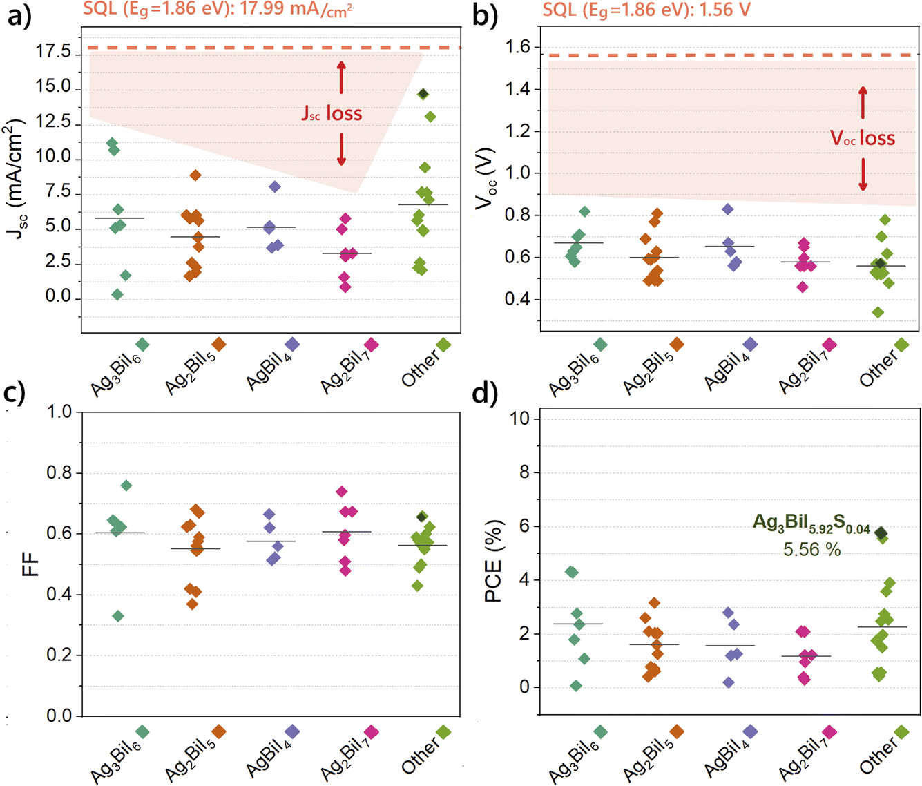 | ||
| Fig. 3 Electrical parameters Jsc (a), Voc (b), FF (c), and PCE (d) for the most common SBI compounds Ag3BiI6, Ag2BiI5, AgBiI4, Ag2BiI7, and other SBI-related compounds reported over the years (full table is given in ESI, Table S1†). For reference, dashed lines refer to the values of the SQL theoretical limit for Ag2BiI5 (Eg: 1.86 eV19). Parameters of the champion SBI solar cell are marked in dark green. | ||
One notable observation from Fig. 3 is that among all parameters, the Jsc exhibits the greatest deviation, yet it has the potential to approach the SQL.20,51 For all compounds, the Voc generally varies between 0.5 eV and 0.8 eV, while the FF ranges from 0.5 to 0.7. These factors contribute to a low PCE, which averages at 1.75%. However, recent advancements have enabled SBI solar cells to achieve values up to 2%.19,25,32,42
It is known that recombination at the interface can detrimentally affect Voc. Previous researchers have shown that the addition of a spike layer is effective to reduce recombination. This structure is obtained when the conduction band minimum (CBM) of the ETL is higher than the CBM of the light absorber.46,47 Improvements in Voc have also been achieved by modifying the ETL; for instance, pre-treating the SnO2 layer with SnCl2 for cells with Ag2BiI5 as the absorber enabled achieving a high Voc of 0.81 V.19 The formation of an amorphous SnOx layer has been proven to reduce charge recombination at the interface.47 Doping AgBiI4 with lithium bis(trifluoromethanesulfonyl)imide (Li-TFSI) also improved the Voc for planar heterojunctions, significantly enhancing the FF; in this case, TFSI− anions are responsible for improving the morphology, assisting in the film growth.31 Devices with different configurations have demonstrated enhanced Voc values. For example, when a compact layer of TiO2 and carbon electrodes were employed in Ag2BiI5 devices treated with air blowing, the open-circuit voltage reached 0.77 V.39 Furthermore, in the case of planar inverted Ag3BiI6 devices using NiOx and PCBM/C60, the open-circuit voltage achieved values of 0.82 V and 0.77 V, respectively.48
Comparatively, the Jsc values are subject to change considerably more than the Voc and FF values. Therefore, improving Jsc is pivotal to enhancing the conversion efficiency of SBI solar cells. Three major strategies have been advocated for this purpose. The first strategy involves enhancing Jsc by employing mesoporous structures instead of planar heterojunctions, a method we have previously demonstrated.49 Second, replacing some of the materials in the SBI composition, as referred to in the “Others” category in Fig. 3, has proven to be beneficial. The highest efficiency among SBI-based solar cells has been achieved with the compound Ag3BiI5.92S0.04, obtained from a mixture of Ag3BiI6 and 4% bismuth(III) tris(4-methylbenzodithioate) (C24H21BiS6, referred to as Bi(S2CAr)3 by the authors). Importantly, this sulfur-doped composition also exhibits higher Voc and FF values compared to other compositions (Ag3BiI6, Ag2BiI5, AgBiI4, and AgBi2I7).20
Incorporating elements other than sulfur in the synthesis of SBI also demonstrated an improvement in solar cell efficiency. Specifically, the partial replacement with copper cations has been shown to increase the Jsc of Ag2BiI5 from 6.04 mA cm−2 to 7.13 mA cm−2. This enhancement is achieved by replacing a portion of AgI with copper iodide (CuI) as the starting material, resulting in mixed Ag2−xCuxBiI5 (x = from 0.03 to 0.2), which leads to an increased absorption coefficient.25 The use of antimony has also been reported to enhance the morphology of AgBi2I7 and increase the conversion efficiency from 0.3% to 1.76%.26 Previous studies using halides other than iodine are relatively uncommon. However, it was observed that incorporation of Br into AgBiI4 led to the formation of AgBi(I1−xBrx)4, which improved the morphology and FF.50 Finally, employing bulk heterostructures has proven beneficial: the Ag3Bi2I9/CsBiI9 bulk heterojunction exhibits superior performance compared to standalone SBI device, improving both Voc and Jsc and achieving a conversion efficiency of 3.59%.51
Up to this point, photoconversion layers composed of Ag–Bi–I even with appropriate material ratios and morphology have yet to match the high conversion efficiencies observed in organic–inorganic lead halide perovskite solar cells. The guidelines for achieving high efficiency in SBI solar cells remain largely unknown, suggesting that other crucial factors may be influencing the performance. This paper aims to elucidate the issues encountered with SBI films and discuss how each issue individually impacts the overall performance.
Addressing issues
Since the state of the art has been outlined, this discussion focuses on the issues potentially impacting SBI solar cells. The sections are divided based on common issues identified by previous researchers, aiming to understand the underlying problems in applying SBI to solar cells.Crystal structure and composition
SBI crystals have been reported to exhibit two distinct crystal systems depending on their composition. For Ag-rich materials such as Ag3BiI6 or Ag2BiI5, a trigonal (rhombohedral) structure (R![[3 with combining macron]](https://www.rsc.org/images/entities/char_0033_0304.gif) m) is preferred, while a cubic structure (Fdm) is observed in Bi-rich materials like AgBi2I7 or AgBiI4. There is disagreement regarding the structure of Ag2BiI7, with initial studies suggesting that it forms a cubic structure akin to the ThZr2H7 type.16 However, Mitzi and Yan group showed that this structure is unstable due to the short Bi–I bonds and that Ag2BiI7 is likely to take the Ag-deficient AgBiI4 structure (cubic structure, Fdm).52 Intrinsic investigation of the relationship between the composition and crystal structure has been conducted using Ag4−6xBi2xI4, and a rhombohedral to cubic transition was observed depending on the AgI:BiI3 ratio used.53 From the above, it is expected that the Ag–Bi–I crystalline material is a thermodynamically random solid solution of each ion and that the resulting crystalline system varies due to slight compositional deviations associated with temperature effects.54,55
m) is preferred, while a cubic structure (Fdm) is observed in Bi-rich materials like AgBi2I7 or AgBiI4. There is disagreement regarding the structure of Ag2BiI7, with initial studies suggesting that it forms a cubic structure akin to the ThZr2H7 type.16 However, Mitzi and Yan group showed that this structure is unstable due to the short Bi–I bonds and that Ag2BiI7 is likely to take the Ag-deficient AgBiI4 structure (cubic structure, Fdm).52 Intrinsic investigation of the relationship between the composition and crystal structure has been conducted using Ag4−6xBi2xI4, and a rhombohedral to cubic transition was observed depending on the AgI:BiI3 ratio used.53 From the above, it is expected that the Ag–Bi–I crystalline material is a thermodynamically random solid solution of each ion and that the resulting crystalline system varies due to slight compositional deviations associated with temperature effects.54,55
The potential for the formation of multiple SBI phases, utilizing AgI and BiI3 as starting materials, warrants consideration. Mashadieva et al. have highlighted in their study on the AgI–BiI3 system that Ag3BiI6 and AgBiI4 might constitute a mixture of Ag2BiI5 and AgBi2I7.55 The occurrence of various SBI compounds in AgBiI4 films43 has been documented previously, and the formation of Ag3BiI6 and AgBiI4 is also anticipated based on calculations.56,58 It should be emphasized that X-ray diffraction (XRD) measurements might not discern SBI crystals of varying compositions when mixed, due to the similarity in SBI peaks (Fig. 4). Therefore, one issue is the potential formation of multiple SBI phases during synthesis of a specific SBI film. The small variation in bandgaps among SBI compounds may result from the coexistence of multiple Ag–Bi–I structures. Such heterogeneous systems in SBI may be equivalent to phase segregation observed in perovskites, which is detrimental to carrier transport and overall solar cell performance,57 but first it is necessary to confirm SBI purity upon synthesis.
 | ||
| Fig. 4 XRD patterns extracted from crystallographic libraries for SBI compounds. Ag3BiI6 (CCDC 1776740)62 (blue), AgBiI4 (CCDC 1671019)62 (violet), Ag2BiI5 (JCPDS card # 00-035-1025) (orange) and AgBi2I7 (PDF card # 00-034-1372) (pink). | ||
On the other hand, based on the XRD results, it is observed that the SBI compound exhibits two main peaks, primarily located around 12° and 29° (Fig. 4). Depending on whether the structure is rhombohedral or cubic, these peaks are attributed to the (003) and (104) planes, or the (111) and (400) planes, respectively. Simulations predict that the peak at 29° is more intense than that at 12°.56,58 However, numerous studies have reported the opposite.21,30,31,39 It is noteworthy that higher Jsc values are often reported when the experimental XRD pattern aligns with the theoretical XRD pattern, specifically when the intensity of the 29° peak surpasses that of the 12° peak.20,25,35,51 We posit that enhancing crystallinity and the growth of SBI crystals may be a pivotal method to improve their properties. As it has already been observed in LHP,59,60 it could be possible that SBI crystals may exhibit different electrical properties depending on the plane, with the (104) plane potentially offering superior electrical properties compared to the (003) plane. Single crystals are essential for measuring the intrinsic properties of a single plane, and to date, this has been achieved solely through the vertical Bridgman method61 or the solvothermal method.62 Developing a technique to fabricate single crystals from solution with ease is imperative to further the research. Moreover, undertaking a study dedicated to SBI crystallization, particularly on how properties are influenced by the growth of specific planes or SBI purity, would be beneficial. As advocated, a thorough future analysis of SBI necessitates the incorporation of advanced analytical techniques that have yet to be applied. For instance, it has been established that Grazing Incidence Wide Angle X-ray Scattering (GIWAXS)63,64 is instrumental in evaluating the orientation of SBI crystals.19 Additionally, it is posited that Transmission Electron Microscopy (TEM)65 and Electron Backscatter Diffraction (EBSD)66 techniques will be beneficial in the future for accurately characterizing the mixed phases of SBI crystals. However, it is important to consider the potential damage caused by the electron beam.
Ag0 and Bi0 impurities
Impurities in AgI and BiI3 can obstruct crystallization and lead to degradation in quality.67 The existence of metallic bismuth (Bi0) in SBI films has been confirmed.20,36,37 Notably, Bi0 is known to induce bismuth vacancies, adversely impacting the performance of SBI solar cells.17 Conversely, the origin of Bi0 remains a subject of debate. Given the weak nature of Bi–I bonds, Bi0 may form during the crystallization process of the SBI layer.37 Additionally, we identified ion migration as a potential cause for the production of Bi0.36 The possible presence of Bi0 in the contaminated reactants cannot be overlooked. The significance of starting materials' high purity for fabricating solar cells with elevated reproducibility and conversion efficiency has been substantiated for Pb68,69 and Sn70,71 based solar cells. Given the impact of Pb0 on the valence band edge, which induces trap states within the material,72–74 it is reasonable to surmise that the presence of Bi0 would similarly influence the valence band edge, markedly affecting the solar cell's properties.Similarly, the formation of Ag0 poses a significant issue due to its role in charge recombination, negatively impacting the device performance. Ag0 can be formed from AgI, which may remain as an unreacted impurity in SBI. AgI, a material known for its photographic properties, is sensitive to visible light following the reversible reaction Ag+ + efree− ↔ Ag0.75 Through the photographic mechanism, photoexcited free electrons in AgI could be trapped by interstitial Ag+ ions, leading to the formation of Ag. Although this reaction is reversible, both interstitial Ag+ ions and Ag0 can act as recombination centers, reducing the mobility of electrons and holes within the film. XRD analysis of SBI films has revealed trace amounts of AgI as an impurity, depending on the preparation method.17–22,36,53,54,76–79 This underscores the necessity of using high-purity AgI for preparing SBI films to enhance their efficacy as photovoltaic absorbers.
Electron–phonon coupling
Electron–phonon coupling describes how lattice vibrations (phonons) interact with electrons in a solid material. This kind of interaction can explain different properties of semiconductors, but it is mainly important to understand their transport properties. In general, strong phonon scattering detrimentally affects charge-carrier mobility, weakens photoluminescence (PL) and increases recombination.Bismuth-based materials have already been reported to have self-trapping and low carrier mobility due to the interaction of photoexcited carriers with the lattice.80–86 Their presence is related to a low electronic dimensionality of the material, thereby facilitating interactions between charge carriers and the lattice.80,82 In addition, the “soft” nature of silver–halide bonds and the facile structural distortion of bismuth induce the localization of charge carriers through the formation of small polarons.56,81 As a result, a strong electron–phonon interaction is anticipated, leading to the self-trapping of charge, weak PL, and low photovoltaic performance. Specifically, self-trapping or self-localization refers to a charge carrier that becomes trapped due to its interaction with the lattice, leading to the generation of a phonon (Fig. 5). This phenomenon depends on the chemical composition, dimensionality and capacity of structural distortion.80
 | ||
| Fig. 5 Photoluminescence (PL) spectra for SBI compounds (a) Ag3BiI6, (b) Ag2BiI5, (c) AgBiI4, (d) AgBi2I7 and (e) BiI3 measured following 532 nm continuous wave excitation. The measured PL was detected using a cooled Si-CCD in the high-energy range (600–1100 nm) and a cooled InGaAs detector in the low-energy range (950–1600 nm). The PL was fit with a sum of several Lorentzian functions shown in the colored solid line with the individual Lorentzians plotted as shaded area curves. (f) Composition-dependent variation in PLlow/PLhigh (round markers, right axis) calculated as the ratio of the high-energy contribution (area under peak P3) and the low-energy contribution (sum of areas under peaks P1 and P2). Composition-dependent average photon energy Ephoton (square markers, left axis) calculated as the intensity weighted average of the photon emission energy (=ΣNλEλ/ΣNλ, where Nλ is the number of detected photons with energy lying within an interval of width ΔE centered at Eλ, which corresponds to the PL intensity measured at Eλ). Dashed lines are guides to the eye. Reproduced from ref. 86 with permission from Wiley-VCH GmbH, copyright 2024. (g) Schematic of the charge-carrier dynamic processes present across Cu4x(AgBi)1−xI4. μdeloc and μloc correspond to the mobility of delocalized and localized charge carriers, respectively, while kloc is the localization rate. Reproduced from ref. 81 with permission from Wiley-VCH GmbH, copyright 2021. | ||
In SBI compounds, such as Ag3BiI6, Ag2BiI5, AgBiI4 and AgBi2I7, strong electron–phonon interactions have also been observed.83,86 This phenomenon is linked to the presence of segregated Ag-rich and Bi-rich domains, which are responsible for charge carrier localization and exciton self-trapping in SBI.86 Moreover, Lal et al. observed a broad PL emission, which is associated with the strength of charge carrier localization (Fig. 5).86 Increasing the Ag ratio in SBI leads to weaker charge carrier localization and a decrease in PL emission, whereas Bi-rich compounds exhibit stronger charge carrier localization and higher PL emission.
On the other hand, ultrafast spectroscopic measurements revealed carrier-phonon dynamics, showcasing the rapid relaxation of charge carriers towards the band edge, particularly in AgI domains, with nonradiative relaxation occurring swiftly within a constant below 10 ps after photoexcitation, potentially triggering the formation of metallic silver over time from deeply trapped electrons with Ag+.83 Both mechanisms respond to electron–phonon dynamics that may affect Voc in SBI solar cells through trap-assisted recombination.
These experiments align with earlier studies recognizing the limited carrier mobility in SBI films,19,37,83,86 as a result of electron–phonon coupling. Low charge mobility has been found to be associated with self-localization in SBI.86 Furthermore, this consistency is reflected in our observation of an enhanced Jsc in reported studies when employing a mesoporous structure compared to planar heterojunction devices.17,20,22,25,32 Similar to the dynamics observed in dye-sensitized solar cells, the mesoporous structure, with its augmented surface area, facilitates efficient charge collection and injection into the transport layers.49
As mobility is inversely proportional to the effective mass,87,88 replacing bismuth with cations to reduce the effective mass could potentially increase mobility. Likewise, incorporating different elements such as Cu+, Tl3+, or Sb3+ may enhance electronic connectivity, as silver and bismuth cations are commonly observed to exhibit low electronic dimensionality.81,89 Electronic dimensionality refers to the degree of connectivity between atomic orbitals that constitute the lower conduction band (LCB) and upper valence band (UVB).90 In SBI, the conduction band minimum (CBM) is derived from bismuth and iodine p orbitals, while the valence band maximum (VBM) is composed of silver d orbitals and iodine orbitals.91 This electronic configuration is linked to the edge-sharing octahedra crystal structure,92 which results in low connectivity on the conduction band and valence band orbitals, leading to SBI's low electronic dimensionality.
In actuality, it can be seen that the highest performance is exhibited by the SBI mixed structures, where a portion of iodine is substituted with sulfur (S), suggesting a potential association with the improved mobility. Moreover, incorporating ions or molecules capable of contributing to the valence and conduction bands has the potential to enhance the electrical connectivity,90 thereby potentially improving carrier transport. The standalone use of SBI materials may not be suitable for solar cell applications, and we suggest the incorporation of ions into SBI films while simultaneously reducing their effective mass as a promising approach for improvement.
Recombination in SBI
Self-trap recombination, as previously discussed, is evident from the electron–phonon dynamics within SBI. Recombination rates for Ag3BiI6 and AgBiI4 have been recorded as 4.32 × 10⁸ s−1 and 2 × 10⁸ s−1, respectively.83 The comparatively slower recombination rate for Ag3BiI6 relative to that of AgBiI4 could account for its superior performance,51,83 aligning with the distribution of characteristics of solar cell devices illustrated in Fig. 3. Self-trapping is further induced by point defects within the SBI crystal, including vacancies of silver, bismuth, and iodine. Additionally, BiAg antisites have been identified as trapping sites.81 Moreover, vacancies in the SBI structure can further distort the crystal lattice, enhancing electron–phonon coupling. A higher concentration of vacancies has been observed in Bi-rich compounds, contributing to vacancy-mediated lattice softening. This, in turn, leads to stronger charge carrier localization or self-trapped recombination, ultimately reducing carrier mobility.86It has been generally observed that compositions rich in Bi are prone to a higher incidence of vacancy sites, which correlates with lower Voc values.93 The Voc values of SBI solar cells demonstrate a trend wherein configurations rich in Ag exhibit approximately 0.1 V higher than those rich in Bi. This tendency is likely due to the formation of vacancy sites originating from the generation of metallic bismuth (Bi0).
It is observed that the current SBI solar cells exhibit a higher Voc loss compared to lead-based perovskite solar cells.93,94 The formation of small polarons is suggested as a self-trapping phenomenon within the SBI, potentially contributing to performance degradation. Additionally, the ratio of AgI to BiI3 and the generation of point defects during the crystallization process further complicate the issue. A thorough understanding of these aspects could contribute to mitigating voltage drop in SBI compounds.
In our previous research, we explored the behavior of SBI under low light intensities, uncovering the occurrence of bimolecular recombination (between conduction band electrons and valence band holes) in Ag2BiI5.19 Considering previous research, this observed phenomenon may be related to self-trapping in SBI. Although some studies advocate for an optimal thickness of 300 nm for Ag3BiI6 and AgBiI4,58 our findings suggest that increasing the thickness of the absorber leads to increased recombination, resulting in diminished properties.19 This observation is consistent with the reported detrimental effects associated with reduced mobility as the thickness of the absorber layer increases in LHP.95
Bimolecular recombination is more likely to occur in absorbers characterized by low mobility96 and is less affected by material processes. Buizza et al. have documented the emergence of small polaron formation in the copper–silver–bismuth system, which promotes self-localization in Cu4x(AgBi)1−xI4.81 However, they encountered difficulties in identifying a model that corresponds to both experimental outcomes and theoretical expectations. As a result, they propose the occurrence of Langevin-type recombination on the film. Similar behaviour was previously observed in organic solar cells, where discrepancies between recombination constants obtained via simulation and experimental methods were noted.97 To address this difference, a carrier charge concentration gradient may be suggested to explain the disparity between recombination constants.97 However, further research on bismuth-based materials remains limited. For SBI compounds, with small-polaron formation, recombination might occur on a similar basis as documented for the copper–silver–bismuth system. From our observations19 and the established understanding that bimolecular recombination limits the short-circuit current,63 the noted reduction in Jsc with an increasing Bi ratio in SBI solar cells may indicate a heightened incidence of recombination in Bi-rich compounds. Specifically, recombination occurs by self-localization of charges due to electron–phonon coupling. The crystal structure and capacity for distortion play a key role in determining the localization strength. Low mobility, and consequently low PCE, in Bi-rich compounds is associated with a higher vacancy fraction, which increases the susceptibility of SBI to distortions and, in turn, enhances electron–phonon interactions.86
Perspectives
SBI solar cells represent a promising lead-free alternative to lead-based perovskite solar cells, but they require further enhancements to emerge as a viable option. Various studies have shed light on methods to improve the conversion efficiency of SBI solar cells. We assert that adhering to the following strategies could substantially elevate their performance. Primarily, it is crucial to understand the crystallization process of SBI and its direct impact on physical properties. This understanding could improve the reproducibility of the fabrication process and pinpoint areas for improvement. Secondly, given the role of phonon dynamics in potentially limiting the open-circuit voltage, substituting appropriate cations within the SBI framework could diminish recombination rates and enhance carrier extraction efficiency. Additionally, selecting a suitable charge transport layer that aligns with the energy levels is imperative. Herein, we outline our perspective on the future direction for SBI solar cell enhancement.Crystallization process and crystal analysis
The comprehension of the crystallization process in the fabrication of SBI crystal layers is paramount. During the solution process, it is essential to investigate crystallization while heating, as this is key to producing larger crystals and aids in understanding solvent interactions. Exploring additives that could facilitate crystallization represents a promising avenue for further research. Additives such as Lewis bases98 can control crystallization in order to obtain improved SBI films. Aside from solution-based methods, synthesis of SBI can be obtained via a solid-state reaction, grinding and calcination,99 which can reduce impurities due to low solubility.Regulating the growth of specific SBI crystal planes is another critical factor. Selectively generating (003) and (104) planes and evaluating their influence on the charge separation process are fundamental. Moreover, the development of techniques and the enhancement of understanding for the accurate assessment of SBI crystals are essential. While multiple SBI compounds may exist, the precise identification of these compounds using XRD is challenging due to resolution limitations. Furthermore, techniques such as Electron Backscatter Diffraction (EBSD)100 and Transmission Electron Microscopy (TEM) could be appropriate for directly determining the SBI crystal system. However, these techniques involve high-energy measurements, which pose a risk of damaging SBI crystals, necessitating careful handling during analysis.65
On the other hand, X-ray Photoelectron Spectroscopy (XPS) is a valuable method for determining the Ag:Bi:I ratio. This technique not only enables the measurement of elemental composition but also simultaneously identifies the valence states of each element. It is effective in detecting metallic states such as Ag0 and Bi0. Additionally, a notable advantage of this method is its capability for mapping analysis. Furthermore, Kelvin Probe Force Microscopy (KFM) is a promising technique for verifying the presence of materials with different compositions,101 as it facilitates the visualization of potential differences. In addition, bulk techniques such as inductively coupled plasma mass spectrometry (ICP-MS) and inductively coupled plasma optical emission spectrometry (ICP-OES), in combination with spatially resolved techniques such as laser ablation ICP-MS (LA-ICP-MS), are considered promising tools for measuring the Ag:Bi:I ratio.
Improving mobility and decreasing recombination
The limited charge mobility in SBI is ascribed to pronounced electron–phonon coupling. Improvements in charge mobility are achieved by enhancing the grain size through solution engineering; however, even with low mobility, charge collection efficiency can be improved through strategic decisions regarding the device structure, such as employing mesoporous structures. The introduction of mesoporous materials enhances carrier collection and provides an opportunity to explore promising materials, such as mesoporous SnO2102 and nanotubes,103 to enhance carrier transport. Moreover, strategies for synthesizing uniformly dispersed nanocrystals, as exemplified by AgBiS2, can enhance electrical dimensionality, ultimately leading to higher charge mobility within the film.104
Furthermore, the presence of AgI can lead to the formation of Ag0, which may act as a recombination center, necessitating a reduction in impurity content within the film. It has been observed that solution processing induces the formation of AgI impurities due to the limited solubility of precursor materials. In this regard, a mixed DMSO:DMF solvent system has been shown to enhance the solubility of AgI compared to DMF alone. Moreover, the use of additives or alternative solvents, such as the incorporation of iodine, has been reported to enhance AgI solubility,105,106 thereby facilitating improved crystallization. On the other hand, solid-state reaction methods have exhibited a significant reduction in AgI impurities, suggesting that this approach could be a viable alternative for fabricating SBI films with higher purity.
Decreasing electron–phonon coupling behaviour
“Pure” SBI, composed solely of Ag, Bi, and I, might not be a practical option due to the possible impediment of charge transfer by polaron formation, leading to a reduction in conversion efficiency. Reduction in effective mass could be realized through the cation exchange process, in which a portion of Ag+ and/or Bi3+ ions are replaced by ions such as Cu+, Rb+, and/or Sb3+. The use of a mixed structure with SBI serving as the base framework offers diverse pathways for carrier movement, thereby enhancing charge transfer efficiency. Moreover, since vacancies may be responsible for stronger polaronic effects that enhance self-localization and decrease mobility in SBI,86 it is primordial to obtain SBI films without impurities that could lead to the formation of vacancies.Recently, it has been shown that applying pressure to Cs2AgBiCl6 diminishes electron–phonon coupling, maintaining the crystal structure and enhancing the PL lifetime.107 Investigating whether SBI crystals exhibit similar behavior could offer a novel avenue to boost the performance of photovoltaic systems.
Scaling up SBI
The research on SBI-based solar cells remains in its early stages; however, it is crucial to consider the feasibility of scaling up for future large-area applications. One of the primary challenges in upscaling is the presence of AgI impurities, which become more likely as the active area expands, ultimately leading to a decline in efficiency. Therefore, controlling impurity formation during synthesis and optimizing film uniformity are essential steps to ensure stable performance in larger area devices.Another critical factor in scaling up is the selection of an appropriate fabrication method. While conventional solution processes such as spin coating are effective for small scale fabrication, they may not be suitable for large-area production.108 Alternative deposition techniques, such as inkjet printing, could serve as a viable approach for the coating process in SBI thin films. Therefore, careful consideration should be given to the significant impact of the low solubility of AgI. The strategic development of additives that improve the solubility of AgI may be the key to achieving large-area fabrication of solar cells.
Conclusions and outlook
SBI crystals, being solely composed of inorganic materials, exhibit relative resistance to moisture and oxygen, suggesting their potential for excellent durability. This characteristic is particularly relevant for flexible device applications, where plastic film substrates are permeable to oxygen and moisture. Moreover, compared to other lead-free materials, SBI still exhibits lower efficiency compared to other lead-free materials. Currently, silver bismuth sulfide (AgBiS2) solar cells achieve efficiencies of around 9%,104 while Cs-based perovskites have reached 11%.109Given its bandgap and documented success in indoor applications,19,110,111 SBI's utility could be optimally exploited in this domain, contrasting with terrestrial applications where perovskites are viewed as formidable contenders. To harness this potential, selecting a suitable HTL and ETL tailored for indoor conditions is imperative.
The most pressing issue is the low conversion efficiency; addressing this challenge requires a more comprehensive understanding of the fundamental properties of SBI, including its formation process and its effect on efficiency. It is essential to investigate the presence of multiple SBI compounds in the film and determine whether the optoelectronic properties vary depending on the growth orientation of SBI. These fundamental insights will provide the foundation for developing effective strategies to enhance performance.
For now, the incorporation of mixed structures has shown potential for improving efficiency by enhancing charge carrier mobility. Furthermore, decreasing impurities on SBI films and the use of mixed structures can mitigate the effects of electron–phonon coupling.92 Through continuous and innovative research efforts in compositional and interfacial engineering to improve carrier mobility, there is promising potential to overcome and address this significant challenge.
Data availability
Data for this article, including Table S1 of SBI efficiencies and parameters through the years are available at ESI at https://doi.org/10.1039/D4SC07955H.†Author contributions
N. B. C. G. and S. N. conceived the idea. N. B. C. G. conducted the literature review, analysed the published results, and wrote the manuscript. T. M. and S. N. provided key advice and supervised the preparation of the text. All authors discussed and commented on the manuscript.Conflicts of interest
There are no conflicts to declare.Acknowledgements
The present research has been supported by the Japan Society for the Promotion of Science with Grants-in-Aid for Scientific Research (No. 24K08273 and 24H00488). The authors acknowledge financial support from Citizen Watch Co., Ltd. N. S. was supported by the Science Research Promotion Fund of The Promotion and Mutual Aid Corporation for Private Schools of Japan.Notes and references
- A. Kojima, K. Teshima, Y. Shirai and T. Miyasaka, J. Am. Chem. Soc., 2009, 131, 6050 CrossRef CAS.
- NREL, Chart of Best Research-Cell Efficiencies Provided by NREL, https://www.nrel.gov/pv/cell-efficiency.html.
- E. Aydin, E. Ugur, B. K. Yildirim, T. G. Allen, P. Dally, A. Razzaq, F. Cao, L. Xu, B. Vishal, A. Yazmaciyan, A. A. Said, S. Zhumagali, R. Azmi, M. Babics, A. Fell, C. Xiao and S. De Wolf, Nature, 2023, 623, 732 CrossRef CAS PubMed.
- Q. Jiang, R. Tirawat, R. A. Kerner, E. A. Gaulding, Y. Xian, X. Wang, J. M. Newkirk, Y. Yan, J. J. Berry and K. Zhu, Nature, 2023, 623, 313 CrossRef CAS PubMed.
- S. P. Dunfield, L. Bliss, F. Zhang, J. M. Luther, K. Zhu, M. F. A. M. van Hest, M. O. Reese and J. J. Berry, From Defects to Degradation: A Mechanistic Understanding of Degradation in Perovskite Solar Cell Devices and Modules, Adv. Energy Mater., 2020, 10, 1904054 CrossRef CAS.
- Y. Zhao, H. Xiang, R. Ran, W. Zhou, W. Wang and Z. Shao, J. Energy Chem., 2023, 83, 189 CrossRef CAS.
- H. Zhang, L. Pfeifer, S. M. Zakeeruddin, J. Chu and M. Grätzel, Nat. Rev. Chem, 2023, 7, 632 CrossRef CAS.
- B. Chen, C. Fei, S. Chen, H. Gu, X. Xiao and J. Huang, Nat. Commun., 2021, 12, 5859 CrossRef CAS.
- J. Dou, Y. Bai and Q. Chen, Mater. Chem. Front., 2022, 6, 2779 Search PubMed.
- C. H. Chen, S. N. Cheng, L. Cheng, Z. K. Wang and L. S. Liao, Adv. Energy Mater., 2023, 13, 2204144 CrossRef CAS.
- N. K. Tailor, A. Listorti, S. Colella and S. Satapathi, Adv. Mater. Technol., 2023, 8, 2200442 CrossRef CAS.
- U. Farooq, M. Zhang, D. Chi, J. Wang, A. M. Idris, S. Huang, Z. Pan and Z. Li, ACS Appl. Energy Mater., 2023, 6, 10294 CrossRef CAS.
- A. Raj, M. Kumar and A. Anshul, Phys. Status Solidi A, 2022, 219, 2200425 CrossRef CAS.
- A. Abate, Stable Tin-Based Perovskite Solar Cells, ACS Energy Lett., 2023, 8, 1896 CrossRef CAS PubMed.
- T. Imran, S. Rauf, H. Raza, L. Aziz, R. Chen, S. Liu, J. Wang, M. A. Ahmad, S. Zhang, Y. Zhang, Z. Liu and W. Chen, Adv. Energy Mater., 2022, 12, 2200305 Search PubMed.
- Y. Kim, Z. Yang, A. Jain, O. Voznyy, G.-H. Kim, M. Liu, L. N. Quan, F. P. García de Arquer, R. Comin, J. Z. Fan and E. H. Sargent, Angew. Chem., 2016, 128, 9738 CrossRef.
- I. Turkevych, S. Kazaoui, E. Ito, T. Urano, K. Yamada, H. Tomiyasu, H. Yamagishi, M. Kondo and S. Aramaki, ChemSusChem, 2017, 10, 3754 CrossRef CAS.
- A. Bera, S. Paramanik, A. Maiti and A. J. Pal, Phys. Rev. Mater., 2021, 5, 095404 CrossRef CAS.
- N. B. Correa Guerrero, Z. Guo, N. Shibayama, A. K. Jena and T. Miyasaka, ACS Appl. Energy Mater., 2023, 6, 10274 CrossRef CAS.
- N. Pai, J. Lu, T. R. Gengenbach, A. Seeber, A. S. R. Chesman, L. Jiang, D. C. Senevirathna, P. C. Andrews, U. Bach, Y. B. Cheng and A. N. Simonov, Adv. Energy Mater., 2019, 9, 1803396 CrossRef.
- B. Ghosh, B. Wu, X. Guo, P. C. Harikesh, R. A. John, T. Baikie, Arramel, A. T. S. Wee, C. Guet, T. C. Sum, S. Mhaisalkar and N. Mathews, Adv. Energy Mater., 2018, 8, 1802051 CrossRef.
- F. Iyoda, R. Nishikubo, A. Wakamiya and A. Saeki, ACS Appl. Energy Mater., 2020, 3, 8224 Search PubMed.
- Y. Yuan and N. Robertson, Sustainable Energy Fuels, 2023, 7, 1067 RSC.
- C. Nishikawa, R. Nishikubo, F. Ishiwari and A. Saeki, ACS Appl. Energy Mater., 2022, 5, 6291 CrossRef CAS.
- J. W. Park, Y. Lim, K. Y. Doh, M. T. Jung, Y. I. Jeon, I. S. Yang, H. S. Choi, J. Kim, D. Lee and W. I. Lee, Sustainable Energy Fuels, 2021, 5, 1439 RSC.
- H. Zhu, A. Erbing, H. Wu, G. J. Man, S. Mukherjee, C. Kamal, M. B. Johansson, H. Rensmo, M. Odelius and E. M. J. Johansson, ACS Appl. Energy Mater., 2020, 3, 7372 CrossRef CAS.
- H. Zhu, I. Turkevych, H. Lohan, P. Liu, R. W. Martin, F. C. P. Massabuau and R. L. Z. Hoye, Int. Mater. Rev., 2024, 69, 19 CrossRef CAS.
- A. Chakraborty, N. Pai, J. Zhao, B. R. Tuttle, A. N. Simonov and V. Pecunia, Adv. Funct. Mater., 2022, 32, 2203300 CrossRef CAS.
- Y. Cui, L. Yang, X. Wu, J. Deng, X. Zhang and J. Zhang, J. Mater. Chem. C, 2022, 10, 16629 RSC.
- W. Zhai, L. Huang, X. Cui, G. Li, Z. Zhang, P. Chen, Y. Li, Y. Tang, L. Lin, Z. Yan and J. M. Liu, J. Mater. Chem. C, 2022, 10, 5321 RSC.
- Q. Zhang, C. Wu, X. Qi, F. Lv, Z. Zhang, Y. Liu, S. Wang, B. Qu, Z. Chen and L. Xiao, ACS Appl. Energy Mater., 2019, 2, 3651 CrossRef CAS.
- K. C. Hsiao, Y. F. Yu, C. M. Ho, M. H. Jao, Y. H. Chang, S. H. Chen, Y. H. Chang, W. F. Su, K. M. Lee and M. C. Wu, Chem. Eng. J., 2023, 451, 138807 CrossRef CAS.
- P. Kumar, K. Ahmad and S. M. Mobin, Nanoscale Adv., 2023, 5, 1624 RSC.
- M. S. Shadabroo, H. Abdizadeh, M. Shabani and M. R. Golobostanfard, Inorg. Chem., 2021, 60, 11110 CrossRef CAS.
- H. Zhu, M. Pan, M. B. Johansson and E. M. J. Johansson, ChemSusChem, 2017, 10, 2592 CrossRef CAS PubMed.
- A. Kulkarni, F. Ünlü, N. Pant, J. Kaur, C. Bohr, A. K. Jena, S. Öz, M. Yanagida, Y. Shirai, M. Ikegami, K. Miyano, Y. Tachibana, S. Chakraborty, S. Mathur and T. Miyasaka, Sol. RRL, 2021, 5, 2100077 CrossRef CAS.
- A. Mutlu and C. Zafer, Sol. Energy, 2022, 234, 190 CrossRef CAS.
- A. Crovetto, A. Hajijafarassar, O. Hansen, B. Seger, I. Chorkendorff and P. C. K. Vesborg, Chem. Mater., 2020, 32, 3385 CrossRef CAS.
- F. He, Q. Wang, W. Zhu, D. Chen, J. Zhang, C. Zhang and Y. Hao, Solid-State Electron., 2021, 176, 107950 CrossRef CAS.
- K. W. Jung, M. R. Sohn, H. M. Lee, I. S. Yang, S. Do Sung, J. Kim, E. Wei-Guang Diau and W. I. Lee, Sustainable Energy Fuels, 2018, 2, 294 RSC.
- A. Kulkarni, A. K. Jena, M. Ikegami and T. Miyasaka, Chem. Commun., 2019, 55, 4031 RSC.
- M. C. Wu, Q. H. Wang, K. C. Hsiao, S. H. Chen, C. M. Ho, M. H. Jao, Y. H. Chang and W. F. Su, Chem. Eng. J. Adv., 2022, 10, 100275 CrossRef CAS.
- H. Ye, Z. Liu, H. Han, T. Shi and G. Liao, Mater. Adv., 2022, 3, 7248 RSC.
- M. Xiao, F. Huang, W. Huang, Y. Dkhissi, Y. Zhu, J. Etheridge, A. Gray-Weale, U. Bach, Y. B. Cheng and L. Spiccia, Angew. Chem., Int. Ed., 2014, 53, 9898 CrossRef CAS.
- N. J. Jeon, J. H. Noh, Y. C. Kim, W. S. Yang, S. Ryu and S. Il Seok, Nat. Mater., 2014, 13, 897 CrossRef CAS.
- C. Ding, Y. Zhang, F. Liu, Y. Kitabatake, S. Hayase, T. Toyoda, K. Yoshino, T. Minemoto, K. Katayama and Q. Shen, Nano Energy, 2018, 53, 17 CrossRef CAS.
- Z. Guo, A. K. Jena, I. Takei, G. M. Kim, M. A. Kamarudin, Y. Sanehira, A. Ishii, Y. Numata, S. Hayase and T. Miyasaka, J. Am. Chem. Soc., 2020, 142, 9725 CrossRef CAS.
- Y. Seo, S. R. Ha, S. Yoon, S. M. Jeong, H. Choi and D. W. Kang, J. Power Sources, 2020, 453, 227903 CrossRef CAS.
- W. Li, J. Liu and D. Zhao, Nat. Rev. Mater., 2016, 1, 16023 CrossRef CAS.
- B. C. Jeon, J. Kim and T. Moon, ChemistrySelect, 2024, 9, e202400337 CrossRef CAS.
- W. Hu, X. He, Z. Fang, W. Lian, Y. Shang, X. Li, W. Zhou, M. Zhang, T. Chen, Y. Lu, L. Zhang, L. Ding and S. Yang, Nano Energy, 2020, 68, 104362 CrossRef CAS.
- Z. Xiao, W. Meng, D. B. Mitzi and Y. Yan, J. Phys. Chem. Lett., 2016, 7, 3903 CrossRef CAS.
- A. Koedtruad, M. Goto, M. Amano Patino, Z. Tan, H. Guo, T. Nakamura, T. Handa, W. T. Chen, Y. C. Chuang, H. S. Sheu, T. Saito, D. Kan, Y. Kanemitsu, A. Wakamiya and Y. Shimakawa, J. Mater. Chem. A, 2019, 7, 5583 RSC.
- Y. Nakamura, N. Shibayama, A. Hori, T. Matsushita, H. Segawa and T. Kondo, Inorg. Chem., 2020, 59, 6709 CrossRef CAS PubMed.
- L. F. Mashadieva, Z. S. Aliev, A. V. Shevelkov and M. B. Babanly, J. Alloys Compd., 2013, 551, 512 CrossRef CAS.
- V. T. Barone, B. R. Tuttle and S. V. Khare, J. Appl. Phys., 2022, 131, 245701 CrossRef CAS.
- J. T. Dubose and P. V. Kamat, Acc. Mater. Res., 2022, 3, 761 CrossRef CAS.
- B. Cucco, L. Pedesseau, C. Katan, J. Even, M. Kepenekian and G. Volonakis, Sol. RRL, 2022, 6, 2200718 CrossRef CAS.
- C. Ma, M. Grätzel and N. G. Park, ACS Energy Lett., 2022, 7, 3120 CrossRef CAS.
- C. Ma, T. E. Felix, S.-Ho Lee, D.-H. Kang, S. J. Kwon, M. Grätzel and N.-G. Park, Science, 2023, 379, 173 CrossRef CAS PubMed.
- S. Tie, W. Zhao, W. Huang, D. Xin, M. Zhang, Z. Yang, J. Long, Q. Chen, X. Zheng, J. Zhu and W. H. Zhang, J. Phys. Chem. Lett., 2020, 11, 7939 CrossRef CAS.
- T. Oldag, T. Aussieker, H.-L. Keller, C. Preitschaft and A. Pfitzner, Chem. Inf., 2005, 36, 677 Search PubMed.
- N. Klipfel, C. Momblona, H. Kanda, N. Shibayama, Y. Nakamura, M. D. Mensi, C. Liu, C. Roldán-Carmona and M. K. Nazeeruddin, Sol. RRL, 2021, 5, 2100191 CrossRef CAS.
- Y. Nakamura, N. Shibayama and K. Sugimoto, Chem. Commun., 2021, 57, 2685 RSC.
- T. W. Kim, N. Shibayama, L. Cojocaru, S. Uchida, T. Kondo and H. Segawa, Adv. Funct. Mater., 2018, 28, 1804039 CrossRef.
- H. Fan, J. H. Huang, L. Chen, Y. Zhang, Y. Wang, C. Y. Gao, P. Wang, X. Zhou, K. J. Jiang and Y. L. Song, J. Mater. Chem. A, 2021, 9, 7625 RSC.
- M. Khazaee, K. Sardashti, J. P. Sun, H. Zhou, C. Clegg, I. G. Hill, J. L. Jones, D. C. Lupascu and D. B. Mitzi, Chem. Mater., 2018, 30, 3538 CrossRef CAS.
- J. Yao, L. Yang, F. Cai, Y. Yan, R. S. Gurney, D. Liu and T. Wang, Sustainable Energy Fuels, 2018, 2, 436 RSC.
- D. C. Senevirathna, J. C. Yu, T. A. Nirmal Peiris, B. Li, M. Michalska, H. Li and J. J. Jasieniak, ACS Mater. Lett., 2021, 3, 351 CrossRef CAS.
- F. Gu, S. Ye, Z. Zhao, H. Rao, Z. Liu, Z. Bian and C. Huang, Sol. RRL, 2018, 2, 1800136 CrossRef.
- M. H. Kumar, S. Dharani, W. L. Leong, P. P. Boix, R. R. Prabhakar, T. Baikie, C. Shi, H. Ding, R. Ramesh, M. Asta, M. Graetzel, S. G. Mhaisalkar and N. Mathews, Adv. Mater., 2014, 26, 7122 CrossRef CAS.
- T. Nakamura, Y. Kondo, N. Ohashi, C. Sakamoto, A. Hasegawa, S. Hu, M. A. Truong, R. Murdey, Y. Kanemitsu and A. Wakamiya, Bull. Chem. Soc. Jpn., 2024, 97, uoad025 CrossRef.
- F. S. Zu, P. Amsalem, I. Salzmann, R. Bin Wang, M. Ralaiarisoa, S. Kowarik, S. Duhm and N. Koch, Adv. Opt. Mater., 2017, 5, 1700139 CrossRef.
- G. Sadoughi, D. E. Starr, E. Handick, S. D. Stranks, M. Gorgoi, R. G. Wilks, M. Bär and H. J. Snaith, ACS Appl. Mater. Interfaces, 2015, 7, 13440 CrossRef CAS.
- H. Hada, Y. Yonezawa, A. Yoshida and A. Kurakake, J. Phys. Chem., 1976, 80, 2728 CrossRef CAS.
- M. D. Prasad, M. G. Krishna and S. K. Batabyal, ACS Appl. Nano Mater., 2021, 4, 1252 CrossRef CAS.
- Y. Wang, Y. Liu, X. Shi, L. Huang, J. Tong, G. Wang and D. Pan, New J. Chem., 2021, 45, 14158 RSC.
- M. Khazaee, K. Sardashti, C.-C. Chung, J.-P. Sun, H. Zhou, E. Bergmann, W. A. Dunlap-Shohl, Q. Han, I. G. Hill, J. L. Jones, D. C. Lupascu and D. B. Mitzi, J. Mater. Chem. A, 2019, 7, 2095 RSC.
- A. A. Ramachandran, B. Krishnan, D. A. Avellaneda, M. I. M. Palma, J. A. A. Martinez and S. Shaji, Surf. Interfaces, 2022, 30, 101985 CrossRef CAS.
- L. R. V. Buizza, A. D. Wright, G. Longo, H. C. Sansom, C. Q. Xia, M. J. Rosseinsky, M. B. Johnston, H. J. Snaith and L. M. Herz, ACS Energy Lett., 2021, 6, 1729 CrossRef CAS.
- L. R. V. Buizza, H. C. Sansom, A. D. Wright, A. M. Ulatowski, M. B. Johnston, H. J. Snaith and L. M. Herz, Adv. Funct. Mater., 2022, 32, 2108392 CrossRef CAS.
- X. He, N. K. Tailor, S. Satapathi, J. Brgoch and D.-S. Yang, Adv. Opt. Mater., 2024, 12, 2300199 CrossRef CAS.
- A. Merker, M. Morgenroth, M. Scholz, T. Lenzer and K. Oum, J. Phys. Chem. C, 2023, 127, 1487 CrossRef CAS.
- B. Wu, W. Ning, Q. Xu, M. Manjappa, M. Feng, S. Ye, J. Fu, S. Lie, T. Yin, F. Wang, T. Wee Goh, P. Cholakkal Harikesh, Y. Kang Eugene Tay, Z. Xiang Shen, F. Huang, R. Singh, G. Zhou, F. Gao and T. Chien Sum, Sci. Adv., 2021, 7, eabd3160 CrossRef CAS PubMed.
- J. Leveillee, G. Volonakis and F. Giustino, J. Phys. Chem. Lett., 2021, 12, 4474 CrossRef CAS PubMed.
- S. Lal, M. Righetto, B. W. J. Putland, H. C. Sansom, S. G. Motti, H. Jin, M. B. Johnston, H. J. Snaith and L. M. Herz, Adv. Funct. Mater., 2024, 34, 2315942 CrossRef CAS.
- C. Motta, F. El-Mellouhi and S. Sanvito, Sci. Rep., 2015, 5, 12746 CrossRef CAS PubMed.
- K. M. McCall, Z. Liu, G. Trimarchi, C. C. Stoumpos, W. Lin, Y. He, I. Hadar, M. G. Kanatzidis and B. W. Wessels, ACS Photonics, 2018, 5, 3748 CrossRef CAS.
- F. Ji, G. Boschloo, F. Wang and F. Gao, Sol. RRL, 2023, 7, 2201112 CrossRef CAS.
- Z. Xiao, W. Meng, J. Wang, D. B. Mitzi and Y. Yan, Mater. Horiz., 2017, 4, 206 RSC.
- V. T. Barone, B. R. Tuttle and S. V. Khare, Comput. Mater. Sci., 2024, 231, 112587 CrossRef CAS.
- W. Yu, Y. Zou, H. Wang, S. Qi, C. Wu, X. Guo, Y. Liu, Z. Chen, B. Qu and L. Xiao, Chem. Soc. Rev., 2024, 53, 1769 RSC.
- Z. Guo, A. K. Jena, G. M. Kim and T. Miyasaka, Energy Environ. Sci., 2022, 15, 3171 RSC.
- P. Chen, Y. Bai and L. Wang, Small Struct., 2021, 2, 2000050 CrossRef CAS.
- T. Du, W. Xu, S. Xu, S. R. Ratnasingham, C. T. Lin, J. Kim, J. Briscoe, M. A. McLachlan and J. R. Durrant, J. Mater. Chem. C, 2020, 8, 12648 RSC.
- M. B. Johnston and L. M. Herz, Acc. Chem. Res., 2016, 49, 146 Search PubMed.
- C. Deibel, A. Wagenpfahl and V. Dyakonov, Phys. Rev. B, 2009, 80, 075203 CrossRef.
- W. Zhai, W. Zheng, P. Shi, L. Huang, X. Cui, P. Chen, Y. Tang, L. Lin, Z. Yan and J.-M. Liu, J. Phys. Chem. C, 2024, 128, 8154 CrossRef CAS.
- J. Chang, T. Lin, K. Hsiao, K. Chiang, Y. Chang and M. Wu, Adv. Sci., 2024, 11, 2309526 CrossRef CAS.
- H. Sun, G. W. P. Adhyaksa and E. C. Garnett, Adv. Energy Mater., 2020, 10, 2000364 CrossRef CAS.
- J. Lim, A. I. Rafieh, N. Shibayama, J. Xia, J.-N. Audinot, T. Wirtz, S. Kinge, S. W. Glunz, Y. Ding, B. Ding, H. Kim, M. Saliba, Z. Fei, P. J. Dyson, M. K. Nazeeruddin and H. Kanda, Energy Environ. Sci., 2024, 17, 8209 RSC.
- J. Liu, S. Li, S. Liu, Y. Chu, T. Ye, C. Qiu, Z. Qiu, X. Wang, Y. Wang, Y. Su, Y. Hu, Y. Rong, A. Mei and H. Han, Angew. Chem., Int. Ed., 2022, 61, e202202012 CrossRef CAS.
- M. Zhang and Z. Lin, ACS Energy Lett., 2022, 7, 1260 CrossRef CAS.
- Y. Wang, S. R. Kavanagh, I. Burgués-Ceballos, A. Walsh, D. O. Scanlon and G. Konstantatos, Nat. Photonics, 2022, 16, 235 Search PubMed.
- F. Gaizer, G. Johansson, S. Stølen, A. F. Andresen, J. E. Boggs, F. Lehrich, C. J. Nielsen, D. L. Powell and M. Trætteberg, Acta Chem. Scand., 1988, 42, 259 CrossRef.
- I. L. Mladenovic, W. K. Kegel, P. Bomans and P. M. Frederik, J. Phys. Chem. B, 2003, 107, 5717 CrossRef CAS.
- L. Zhang, Y. Fang, L. Sui, J. Yan, K. Wang, K. Yuan, W. L. Mao and B. Zou, ACS Energy Lett., 2019, 4, 2975 CrossRef CAS.
- P. Zhu, C. Chen, J. Dai, Y. Zhang, R. Mao, S. Chen, J. Huang and J. Zhu, Adv. Mater., 2024, 36, 2307357 CrossRef CAS PubMed.
- I. López-Fernández, D. Valli, C.-Y. Wang, S. Samanta, T. Okamoto, Y.-T. Huang, K. Sun, Y. Liu, V. S. Chirvony, A. Patra, J. Zito, L. De Trizio, D. Gaur, H.-T. Sun, Z. Xia, X. Li, H. Zeng, I. Mora-Seró, N. Pradhan, J. P. Martínez-Pastor, P. Müller-Buschbaum, V. Biju, T. Debnath, M. Saliba, E. Debroye, R. L. Z. Hoye, I. Infante, L. Manna and L. Polavarapu, Adv. Funct. Mater., 2024, 34, 2307896 CrossRef.
- Z. Guo, A. K. Jena and T. Miyasaka, ACS Energy Lett., 2022, 8, 90 Search PubMed.
- I. Turkevych, S. Kazaoui, N. Shirakawa and N. Fukuda, Jpn. J. Appl. Phys., 2021, 60, SCCE06 CrossRef CAS.
Footnote |
| † Electronic supplementary information (ESI) available. See DOI: https://doi.org/10.1039/d4sc07955h |
| This journal is © The Royal Society of Chemistry 2025 |