
Exceptionally low thermal conductivity of poly(3-hexylthiophene) single nanowires†
Yi-Jung Leea,
Kai-Sheng Jenga,
Jiun-Tai Chen*a and
Kien Wen Sun*ab
aDepartment of Applied Chemistry, National Chiao Tung University, 1001 University Road, Hsinchu 30010, Taiwan. E-mail: kwsun@mail.nctu.edu.tw; jtchen@mail.nctu.edu.tw
bDepartment of Electronics Engineering, National Chiao Tung University, 1001 University Road, Hsinchu 30010, Taiwan
First published on 16th October 2015
Abstract
Electrical and thermal conductivity measurements were conducted by using microfabricated four-point probe and T-type nanosensors in a vacuum on poly(3-hexylthiophene) (P3HT) single nanowires prepared by the whisker method. The nanowires had a cross-section of only 5 nm × 15 nm and a length of 0.5–10 μm. The electrical conductance of nanowires was 3.3 × 10⁻⁷ 1/Ω and remained stable even after exposing the wires to ambient conditions for a few days. The thermal conductivity of a nanowire was 0.055 ± 0.003 W m−1 K−1 which was approximately an order of magnitude lower than other previously reported P3HT single nanowires with a diameter of 120 nm and embedded in anodic aluminum oxide matrix. This thermal conductivity was also approximately four times smaller than that of P3HT amorphous thin films (∼0.2 W m−1 K−1). The exceptionally low thermal conductivity was attributed to increased interface-phonon scattering because heat propagation was confined to an extreme narrow spatial dimension.
Organic polymers are attracting considerable attention as plausible thermoelectric materials, because they are semiconductors that exhibit relatively low thermal conductivity. Compared with traditional inorganic thermoelectric materials, organic electronic materials have the noteworthy advantages of being mechanically flexible, low-cost, and solution processable. Given that the thermal conductivities of disorder polymer chains are often an order of magnitude lower than those of silica glass, these polymer chains have been suggested to have thermoelectric applications. A number of conjugated polymers have been studied, including poly(3,4-ethylenedioxythiophene)poly(styrenesulfone) (PEDOT:PSS), [6,6]-phenyl C61-butyric acid methyl ester (PCBM), and poly(3-hexylthiophene) (P3HT).1–6 The effective thermal conductivity of solution-derived P3HT thin films with different thickness on substrates has been investigated by applying 3ω technique.6 Thermal conductivity was 0.189 ± 0.023 W m−1 K−1 for a P3HT layer on glass substrate. Other investigations on highly doped P3HT have reported an average thermal conductivity of 0.48 W m−1 K−1.7 Optical measurement of thermal conductivity was also performed using fiber aligned frequency domain thermoreflectance for a 600 nm parylene film and a 1600 nm P3HT film.8 Thermal conductivities of PCBM thin films have further been shown to be independent of temperature above 180 K and to be <0.03 ± 0.003 W m−1 K−1 at room temperature.4 Moreover, thermal conductivities varying from 0.031 ± 0.005 W m−1 K−1 to 0.227 ± 0.014 W m−1 K−1 near room temperature have been measured by time domain thermoreflectance for PEDOT:PSS, PCBM, P3HT, and P3HT:PCBM blend thin films. The thermal conductivities of conducting polymers are found to be intrinsically lower than those of inorganic materials, which typically range within of 0.1–1 W m−1 K−1. Given the advances in organic optoelectronics over the past few years, large electrical conductivity values and Seebeck coefficients can now be found in some conducting polymers. Large ZT values can be expected when combined with low thermal conductivity.
Among such conducting polymers, P3HT is one of the most intensively studied organic semiconductors because of its unique thermal and electrical properties. It possesses excellent solution processability, chemical stability, and high carrier mobility.9–11 The bandgap energy of P3HT is approximately 1.9 eV, which is in the same range as typical semiconductors. By converting P3HT into nanowires (NWs), a decrease in thermal conductivity of NWs and an improvement in their ZT values are expected because of the reduced dimensionality.5,12,13 A numerical simulation based on the Holstein small-polaron model has been applied to one-dimensional (1D) P3HT and PEDOT:PSS molecular chains to study thermoelectric properties of molecular NWs.12 These 1D NWs are excellent thermoelectric materials because narrow and sharp density of states could increase Seebeck coefficient, and thermal conductivity along the molecule stacking direction could be very small because of enhanced interface-phonon scattering.12 More recently, individual P3HT NWs of three different diameters embedded in a matrix have been investigated by 3ω scanning thermal microscopy. Thermal conductivity decreases when NWs diameters are reduced.5 A thermal conductivity of 0.5 ± 0.24 W m−1 K−1 for intrinsic P3HT NWs 120 nm in diameter has been determined by effective medium theory.
The present work aimed to investigate electrical and thermal characteristics of individual P3HT NWs with a narrow cross-section of 5 nm × 15 nm in a vacuum using a four-point contact probe and T-type nanosensors. The thermal conductivities of the NWs were determined by a 1D heat-conduction method. Results showed that P3HT NW thermal conductivity was exceptionally lower than those for previously reported thin films and NWs with larger diameters, which can be explained by the increase in phonon boundary scattering caused by reduced dimensionality.
P3HT NWs were synthesized by the whisker method reported in ref. 14–17, in which cyclohexanone was used as a marginal solvent to prepare P3HT NWs. This preparation step in whisker method was similar to recrystallization in organic reaction. Given the low solubility of polymers, they were only slightly soluble or even insoluble in marginal solvent at room temperature. After heating the polymer solution, solvent solubility increased and the polymer can be completely dissolved. The polymer solution was then slowly cooled to room temperature. Solubility decreased again upon cooling, and the polymer molecules self-assembled to form NWs.
P3HT (regioregularity: 91–94%) with a weight-average molecular weight (Mw) of 50–70 kg mol−1 and a polydispersity (PDI) of ≈2.0 was used. To fabricate P3HT NWs, 1 wt% P3HT solution in p-xylene was heated to 80 °C for 30 min to completely dissolve P3HT. Subsequently, P3HT solution was cooled to room temperature. Then, P3HT solution was stored at room temperature for 48 hours and P3HT NWs were formed. The NW-containing solution was purified by centrifugation for four times (5000 rpm, 30 min). After each centrifugation, the solution containing amorphous P3HT was removed, and pure p-xylene was added. More details on the preparation and synthesis of P3HT NWs are found in ref. 18. The NWs were 0.5–10 μm long, 5 nm high, and 15 nm wide, as confirmed by AFM, SEM, and TEM images (Fig. 1). NWs with an average diameter up to 32 nm can be fabricated by varying experimental conditions (for example, different temperatures17 or solvents). Latter we found that the thermal conductivity only increased marginally (∼10%) even for a NW with a diameter of ∼32 nm. More details for the synthesis of NWs with different diameters are presented in the ESI† section.
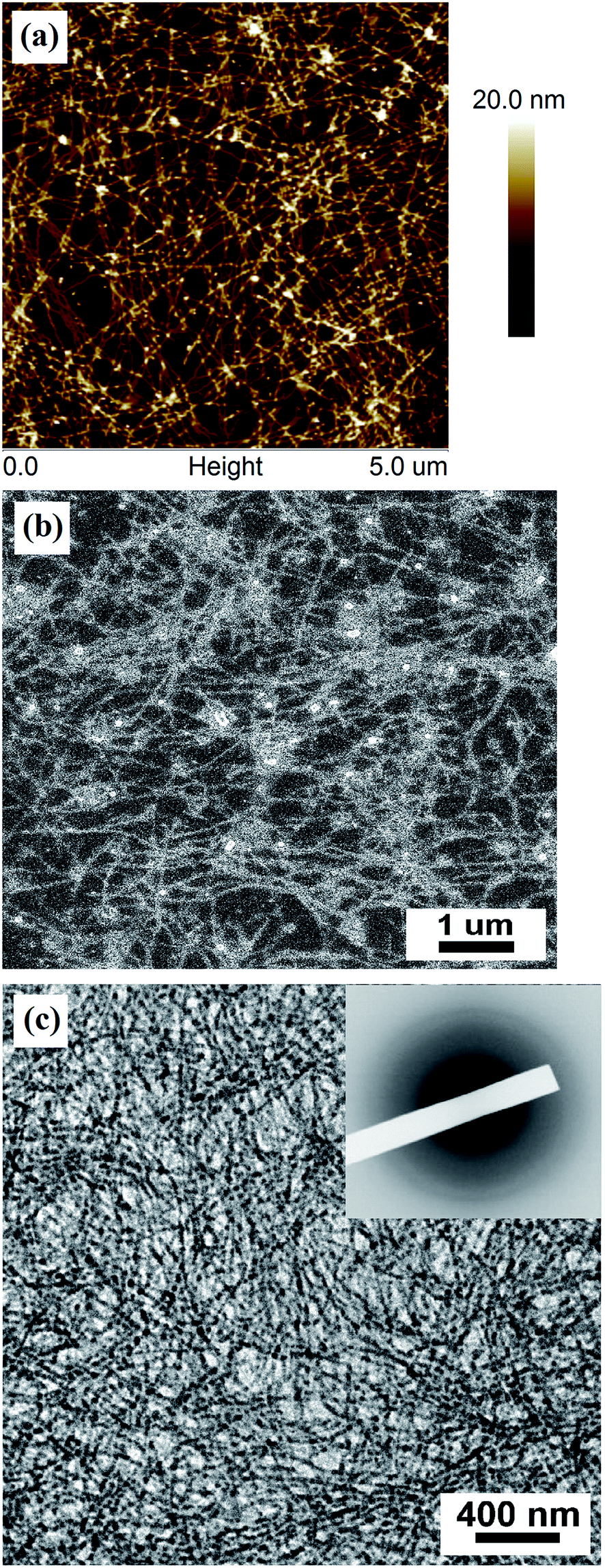 | ||
| Fig. 1 (a) AFM (b) SEM and (c) TEM images of P3HT NWs. Inset in (c) shows the selected area electron diffraction pattern of the P3HT NWs. | ||
A selected area electron diffraction (SAED) pattern of the NWs is displayed in the inset of Fig. 1(c). Although the contrast of the SAED pattern is not very high, however, reflections from (1 0 0), (2 0 0), and (3 0 0) can still be clearly observed. It suggests that that the alkyl side chains of the P3HT NWs are arranged as lamella morphology. The appearance of the peaks from (100), (200), and (300) in the XRD measurements (Fig. S1†) further confirms the conformation of the alkyl side chains of the P3HT NWs. Previous XRD results of P3HT NWs also showed improved crystallinity and orderings of alkyl side chain packing after thermal annealing.18 Schematic of the idea spatial orientation of the P3HT crystallite from the side view of the b axis of the crystal cell (π–π stacking direction) parallel to the NW long axis is illustrated in Fig. S2.† Although the images of P3HT NWs shown in Fig. 1 display fibrillar network structures, single P3HT NWs can be properly separated by spreading diluted nanowires-containing solutions on silicon wafers (Fig. S3†).
A four-point probe on Si templates was then designed and fabricated to measure the conductivity of P3HT single NW. Templates used in experiments were commercially available four-inch silicon wafers with (001) crystal orientation and n-type background doping. After dicing the Si wafer into 2 cm × 2 cm chips, the surface of Si substrate was passivated in advance using a thermally grown 2000 Å-thick SiO2 layer to avoid leakage current through the substrate during current–voltage (I–V) measurements. As shown in Fig. 2(a), a pattern of cross-finger-type Au/Ti wires with a linewidth of 1 μm, a pitch of 1 μm, and a length of 6 μm were defined on Si chip using e-beam lithography within an area of 1 mm2. A drop of diluted P3HT NW in p-xylene solution was placed within electrode patterns. By applying a bias across contact pads, dielectrophoresis force19–22 drove NW to bridge the electrode gap. After a single NW was selected, a focus ion beam (FIB) was used to selectively deposit platinum (Pt) to make contacts with finger electrodes.
 | ||
| Fig. 2 (a) Optical image of cross-finger type four-point probe for measuring electrical conductance of P3HT single NW (b) SEM image of a T-type nanosensor (c) and (d) schematic, dimensions, and cross-section view of fabricated T-type sensor with a single NW attached. | ||
Suspended Au/Ti nanofilm T-type sensors were fabricated on silicon templates following procedures reported in ref. 23 and 24. Dielectrophoresis technique was also applied to position NWs across the electrode gap. After one end of a single P3HT NW was safely attached onto the center of the nanosensor and the other to the heat sink, the devices were placed in a dry box for a few days and then cleaned with acetone to remove p-xylene residue and NWs. Fig. 2(b) and the inset show the SEM image of a T-type nanosensor without NW attached. The schematic, dimensions, and cross-section view of the prepared T-type sensor with a single NW attached are displayed in Fig. 2(c) and (d). The nanosensor acted simultaneously as a heater and a thermometer to measure the average nanosensor temperature such that the local temperature of the junction and the heat input to P3HT NW can be calculated by solving 1-D steady-state heat conduction model.23
For all samples tested, four-point I–V data were linear and symmetrical about zero bias. Electrical stability of P3HT NWs was also verified over an extended period. Table 1 depicts the resistance of a single NW over 6 days in air determined by four-point probe measurements. NWs had an average resistance of ∼3.33 × 10⁷ Ω, which was approximately two order of magnitude lower than P3HT films (with an average resistivity of ∼1.14 × 10⁹ Ω). The NWs also showed atmospheric stability and low surface defect levels.
| Day | Day 1 | Day 2 | Day 3 | Day 4 | Day 5 | Day 6 |
|---|---|---|---|---|---|---|
| Resistance (Ω) | 3.33 × 10⁷ | 3.33 × 10⁷ | 3.32 × 10⁷ | 3.28 × 10⁷ | 3.42 × 10⁷ | 3.32 × 10⁷ |
Before P3HT NWs were attached onto the nanosensor, resistance–temperature coefficient βns (K−1) and thermal conductivity λns (W m−1 K−1) of nanosensor were first be determined. The resistance–temperature relation of nanosensor was measured with a four-point probe, as shown in Fig. 2(b), by supplying a small current to nanosensor. The temperature increase of nanosensor in a vacuum caused by self-heating was less than 8.5 mK. Dimensions of nanosensor were determined with a scanning electron microscope and metal film thickness was measured with a Dektak surface profiler. The measured resistance–temperature coefficients of nanosensor are shown in Fig. 3. The measured βns was significantly lower than bulk values (∼0.039 K−1) of typical metals at 300 K.23,24 The increase in temperature of nanosensor (volumetric average temperature rise ΔTv) when subjected to different currents can be determined from the measurement of resistance using the expression  , where R0 is the electrical resistance of nanofilm at 273 K and βns is the resistance–temperature coefficient of the nanosensor obtained from calibration. The volumetric average temperature rise of nanosensor without P3HT NWs as a function of heating rate (q = IV) is shown in Fig. 4. The thermal conductivity λns (W m−1 K−1) of nanosensor can be calculated using the expression
  by extracting the slope from a linear least-square fit of experimental data, as shown in Fig. 4. qv is the volumetric heat generation rate given by
  , where w, t, and lns are the width, thickness, and length of nanosensor, respectively, I and V are heating current and voltage.
 | ||
| Fig. 3 Resistance–temperature coefficient of nanosensor with thickness, width, and length of 60 nm, 547 nm, and 7.72 μm, respectively. | ||
 | ||
| Fig. 4 Volumetric average temperature rise versus heating rate measured in a vacuum for the nanosensor with and without the presence of a P3HT single NW. | ||
The volumetric average temperature rise of nanosensor as a function of heating rate with a P3HT NW is depicted in Fig. 4. The average temperature rise with a P3HT NW was lower than that without NW. Assuming that thermal contact resistance was negligible,25 the thermal conductivity λNW of a single P3HT NW at room temperature can be calculated from the equation given in ref. 22:

The thermal conductivity obtained from this measurement was compared with previously reported ones for NWs and P3HT thin films. Thermal conductivity measurements were conducted by Muñoz Rojo et al. on P3HT NWs using 3ω scanning thermal microscopy technique operated in contact mode.5 The intrinsic thermal conductivity of individual semicrystalline P3HT NW embedded in the anodic aluminum oxide matrix was deduced by solving an equation derived from effective medium theory.26,27 They observed a reduction of thermal conductivity from ∼2.29 W m−1 K−1 to ∼0.5 W m−1 K−1 when the diameter of NWs was reduced from 350 nm to 120 nm. The exceptionally high thermal conductivities in this experiment were attributed to well-aligned polymeric chains in contrast to disordered ones. However, our results showed nearly an order of magnitude lower thermal conductivity when the cross-section of NWs was reduced to 5 nm × 15 nm. Thermal conductivity decreased with decreased NW diameter, indicating that phonon transport through P3HT NW was suppressed because of the strong phonon boundary scattering and/or possible changes in phonon dispersion due to enhanced confinement in 1D structure. Duda and co-workers3 reported on the thermal conductivity of P3HT thin films as measured by time domain thermoreflectance. They found a thermal conductivity of ∼0.185 W m−1 K−1 near room temperature, which did not vary with changes in film thickness from 77 nm to 200 nm. Their reported thermal conductivity of P3HT thin film well agreed with previous measurements.6,8 However, the result was still approximately four times higher than our semicrystalline P3HT single NW. A parameter free computational model for characterizing thermoelectric figure of merit (ZT value) of single organic molecular chains was developed by Wang et al.13 using nonequilibrium MD method, Boltzmann transport theory, and deformation potential theory. They estimated ZT values of 1.6 and 1.4 for single P3HT chains with p-doping level of 4 × 105 cm−1 and n-doping level of 4 × 105 cm−1, respectively, assuming a lattice thermal conductivity of 0.2 W m−1 K−1. For the NWs with an exceptionally low thermal conductivity (0.055 W m−1 K−1) in this study, one should expect figure of merit larger than 5 with proper doping levels to enhance electrical transport and at the same time to suppress phonon transport with low-dimensional structures.
In summary, we presented electrical and thermal conductivity measurements of P3HT single NW with a cross-section of 5 nm × 15 nm using microfabricated suspended nanosensor and four-point probe technique. The electrical conductivity of the NWs remained relatively stable over an extended period. The thermal conductivity observed was exceptionally lower than larger-diameter P3HT NWs. Thermal conductivity was also four times smaller than those of amorphous thin films, suggesting that phonon boundary scattering had an appreciable effect on thermal transport in P3HT NWs when 1D confinement was strong. Our research can stimulate further theoretical investigations on the intriguing effect of size on thermal transport in P3HT NWs with very narrow diameters.
Acknowledgements
This work is supported by the Ministry of Science and Technology of the Republic of China (Contract no. NSC 102-2112-M-009-011-MY3) and the Approaching Top University (ATU) Program of the Ministry of Education of the Republic of China.References
- D. E. Motaung, G. F. Malgas, C. J. Arendse, S. E. Mavundla and D. Knoesen, Mater. Chem. Phys., 2009, 116, 279–283 CrossRef CAS PubMed.
- M. He, J. Ge, Z. Lin, X. Feng, X. Wang, H. Lu, Y. Yang and F. Qiu, Energy Environ. Sci., 2012, 5, 8351–8358 CAS.
- J. C. Duda, P. E. Hopkins, Y. Shen and M. C. Gupta, Appl. Phys. Lett., 2013, 102, 251912 CrossRef PubMed.
- J. C. Duda, P. E. Hopkins, Y. Shen and M. C. Gupta, Phys. Rev. Lett., 2013, 110, 015902 CrossRef.
- M. Muñoz Rojo, J. Martin, S. Grauby, T. Borca-Tasciuc, S. Dilhaire and M. Martin-Gonzalez, Nanoscale, 2014, 6, 7858–7865 RSC.
- S. Rausch, D. Rauh, C. Deibel, S. Vidi and H. P. Ebert, Int. J. Thermophys., 2013, 34, 820–830 CrossRef CAS.
- J. Sun, M.-L. Yeh, B. J. Jung, B. Zhang, J. Feser, A. Majumdar and H. E. Katz, Macromolecules, 2010, 43, 2897 CrossRef CAS.
- J. A. Malen, K. Baheti, T. Tong, Y. Zhao, J. A. Hudgins and A. Majumdar, Journal Of Heat Transfer-Transactions Of The Asme, 2011, 133, 081601 CrossRef.
- M. He, W. Han, J. Ge, Y. L. Yang, F. Qiu and Z. Q. Lin, Energy Environ. Sci., 2011, 4, 2894–2902 CAS.
- M. He, W. Han, J. Ge, W. J. Yu, Y. L. Yang, F. Qiu and Z. Q. Lin, Nanoscale, 2011, 3, 3159–3163 RSC.
- M. He, L. Zhao, J. Wang, W. Han, Y. L. Yang, F. Qiu and Z. Q. Lin, ACS Nano, 2010, 4, 3241–3247 CrossRef CAS PubMed.
- Y. Wang, J. Zhou and R. Yang, J. Phys. Chem. C, 2011, 115, 24418–24428 CAS.
- D. Wang, W. Shi, J. Chen, J. Xi and Z. Shuai, Phys. Chem. Chem. Phys., 2012, 14, 16505–16520 RSC.
- K. J. Ihn, J. Moulton and P. Smith, J. Polym. Sci., Part B: Polym. Phys., 1993, 31, 735–742 CrossRef CAS PubMed.
- W. D. Oosterbaan, V. Vrindts, S. Berson, S. Guillerez, O. Douhéret, B. Ruttens, J. D'Haen, P. Adriaensens, J. Manca, L. Lutsen and D. Vanderzande, J. Mater. Chem., 2009, 19, 5424–5435 RSC.
- S. Berson, R. de Bettignies, S. Bailly and S. Guillerez, Adv. Funct. Mater., 2007, 17, 1377–1384 CrossRef CAS PubMed.
- J. Liu, M. Arif, J. Zou, S. I. Khondaker and L. Zhai, Macromolecules, 2009, 42, 9390–9393 CrossRef CAS.
- C.-M. Fu, K.-S. Jeng, Y.-H. Li, Y. C. Hsu, M.-H. Chi, W.-B. Jian and J.-T. Chen, Macromol. Chem. Phys., 2015, 216, 59–68 CrossRef CAS PubMed.
- K. Yamamoto, S. Akita and Y. Nakayama, Jpn. J. Appl. Phys., 1996, 35, L917–L918 CAS.
- K. Yamamoto, S. Akita and Y. Nakayama, J. Phys. D: Appl. Phys., 1998, 31, L34–L36 CrossRef CAS.
- W. B. Choi, Y. W. Jin, H. Y. Kim, S. J. Lee, M. J. Yun, J. H. Kang, Y. S. Choi, N. S. Park, N. S. Lee and J. M. Kim, Appl. Phys. Lett., 2001, 78, 1547–1549 CrossRef CAS PubMed.
- J. Suehiro, G. Zhou and M. Hara, J. Phys. D: Appl. Phys., 2003, 36, L109–L114 CrossRef CAS.
- M. Fujii, X. Zhang, H. Xie, H. Ago, K. Takahashi, T. Ikuta, H. Abe and T. Shimizu, Phys. Rev. Lett., 2005, 95, 065502 CrossRef.
- X. Zhang, H. Q. Xie, M. Fijii, H. Ago, K. Takahashi, K. Ikuta, H. Abe and T. Shimizu, Int. J. Thermophys., 2007, 28, 33–43 CrossRef.
- P. Kim, L. Shi, A. Majumdar and P. L. McEuen, Phys. Rev. Lett., 2001, 87, 215502 CrossRef CAS.
- A. I. Persson, Y. K. Koh, D. G. Cahill, L. Samuelson and H. Linke, Nano Lett., 2009, 9, 4484–4488 CrossRef CAS PubMed.
- M. Muñoz Rojo, S. Grauby, J. M. Rampnoux, O. Caballero-Calero, M. S. Martin-González and S. Dilhaire, J. Appl. Phys., 2013, 113, 054308 CrossRef PubMed.
Footnote |
| † Electronic supplementary information (ESI) available. See DOI: 10.1039/c5ra09977c |
| This journal is © The Royal Society of Chemistry 2015 |