
 Open Access Article
 This Open Access Article is licensed under a Creative Commons Attribution-Non Commercial 3.0 Unported Licence
High-performance n-type polymer field-effect transistors with exceptional stability†
Manikanta
Makala‡
 a,
Maciej
Barłóg‡
b,
Derek
Dremann
a,
Salahuddin
Attar
b,
Edgar Gutiérrez
Fernández
cd,
Mohammed
Al-Hashimi
*e and
Oana D.
Jurchescu
*a
a,
Maciej
Barłóg‡
b,
Derek
Dremann
a,
Salahuddin
Attar
b,
Edgar Gutiérrez
Fernández
cd,
Mohammed
Al-Hashimi
*e and
Oana D.
Jurchescu
*a
aDepartment of Physics and Center for Functional Materials (CFM), Wake Forest University, Winston Salem, NC 27019, USA. E-mail: jurchescu@wfu.edu
bDepartment of Chemical Engineering, Texas A&M University at Qatar, P.O. Box 23874, Doha, Qatar. E-mail: Malhashimi@hbku.edu.qa
cDepartment of Physics, University of Warwick, Gibbet Hill Road, Coventry, CV4 7AL, UK
dXMas/BM28-ESRF, 71 Avenue Des Martyrs, Grenoble Cedex F-38043, France
eCollege of Science and Engineering, Hamad Bin Khalifa University, P.O. Box: 34110, Doha, Qatar
First published on 19th September 2024
Abstract
Development of organic field-effect transistors (OFETs) that simultaneously exhibit high-performance and high-stability is critical for complementary integrated circuits and other applications based on organic semiconductors. While progress has been made in enhancing p-channel devices, engineering competitive n-type organic transistors remains a formidable obstacle. Herein, we demonstrate the achievement of high-mobility n-type OFETs with unprecedented operational stability through innovative device and material engineering. Thin film transistors fabricated on donor–acceptor polymers based on indacenodithiazole (IDTz) and diketopyrrolopyrrole (DPP) units exhibit electron mobilities up to 1.3 cm2 V−1 s−1, along with a negligible change in mobility, and threshold voltage shift as low as 0.5 V under continuous bias stress of 60 V for both the gate-source and drain-source voltages persisting for more than 1000 min. These remarkable properties position our OFETs as formidable counterparts to p-type transistors, addressing a longstanding challenge in the field.
1. Introduction
Organic semiconductors (OSCs) have attracted significant interest due to their chemical versatility and unique properties, offering mechanical flexibility, lightweight and cost-effective processing. These attributes make them promising candidates for a range of applications, including organic light-emitting diodes (OLEDs), flexible and wearable electronics, sensors, organic photovoltaics (OPVs), and organic field-effect transistors (OFETs).1–5 OFETs serve as a platform for investigating the mechanism of charge transport in OSCs, and represent the fundamental building blocks of organic electronic circuits.6–8 Over time, advancements in material and device design have resulted in remarkable performance, and charge carrier mobilities exceeding 10 cm2 V−1 s−1 have been reported in both small molecules and polymer OFETs.9–15 However, to establish the applicability of OFETs in real-world applications, it is important to also address their stability when subjected to various stress factors, including electrical, mechanical, chemical, environmental, and thermal stress. While significant progress has been made in enhancing the stability of p-type OFETs, and threshold voltage shifts smaller than 0.2 V have been demonstrated even under aggressive bias stress in ambient conditions,16 the development of n-channel devices has comparatively lagged behind. Nevertheless, the field is rapidly advancing, with more n-type OFETs with mobilities exceeding 1 cm2 V−1 s−1 becoming available, and research into their stability increasingly gaining momentum.13–15,17–21 Among the most investigated acceptor building blocks are diimides functionalized acceptors,19,22–29 diketopyrrolopyrrole (DPP),30–34 isoindigo (IID),35 benzodifurandione-based oligo(p-phenylene vinylene) (BDOPV),20,36–40 showcasing significant progress in optimizing charge transport and environmental stability.41–44 Improving operational stability is equally important, as prolonged bias stress usually leads to instabilities that can significantly impact performance.16,45,46 Device degradation typically manifests as a decrease in charge carrier mobility and drain current, a shift in threshold voltage, and/or an increase in the subthreshold slope and off-current.41 Such changes in the current–voltage (I–V) characteristics hold significant implications for the performance of electronic and optoelectronic applications based on these OFETs. Addressing bias–stress degradation in n-channel OFETs is extremely challenging due to the susceptibility of the semiconductor layer to oxidation, which is further exacerbated under the application of an electric field. This vulnerability arises from the relatively high energy of its lowest unoccupied molecular orbital (LUMO), typically exceeding −4 eV, which makes it prone to reduction by common degradation agents. The processing conditions, the semiconductor film composition and morphology, and device geometry have been shown to impact both the environmental and the bias stress stability of n-channel thin-film transistors based on both small molecule and conjugated polymers (CPs).21,47–53 A threshold voltage shift of 2.9 V has been achieved under moderate bias stress, establishing a benchmark for further advancements in operational stability.49 The current performance gap between n-type and p-type OFETs, particularly in terms of operational stability, poses a significant challenge to the development of high-performance, low-cost integrated circuits (ICs). Achieving a balanced performance between n-type and p-type OFETs is crucial for expanding the design space of organic integrated circuits and accelerating their adoption in mainstream applications. Herein, we strategically engineered the device architecture and the chemical structure of the organic semiconductor to achieve high performance n-channel OFETs with exceptional bias–stress stability. The semiconductor layers consisted of donor–acceptor polymers based on Indacenodithiazole (IDTz) ladder-type core and a DPP acceptor unit flanked via a thiophene donor linker. We optimized polymer configurations through varying the alkylation on their backbone (branched vs. linear chains). By chemically tailoring the electrodes with self-assembled monolayers (SAMs), we tuned the device channel from p- to n-type and achieved a remarkable electron mobility of 1.3 cm2 V−1 s−1 in the most optimized devices. Notably, our n-type OFETs demonstrated exceptional operational stability, as evidenced by the negligible change in mobility and remarkably low threshold voltage shift of ΔVth = 0.5 V attained under prolonged continuous bias stress under high electric fields, which persisted for over 1000 min testing in a vacuum atmosphere.2. Results and discussion
The chemical structures of the IDTz-DPP polymers P1–P3 are illustrated in Fig. 1a. The DPP core has several appealing properties, including excellent stability, strong electron deficiency, great aggregation, flexibility to accommodate long alkyl side chains and good thermal stability.54 In our design, we selected a five-membered heterocycle, i.e. thiophene, as a flanking aromatic unit, which minimizes steric stress onto the DPP core and promotes a highly planar polymer backbone, a critical factor for achieving high charge carrier mobilities.55 The IDTz monomer is the analogue to the widely employed ladder donor unit, indacenodithiophene (IDT), which has been extensively used to create high-performance CPs for various applications, including OFETs.9,56–58 In the case of IDTz, a more electron-deficient thiazole unit replaces the thiophene unit found in IDT and this substitution leads to a deeper LUMO.59–61 Sidechain engineering of conjugated polymers represents a powerful tool for tuning their semiconducting properties.62–64 The sidechains not only enhance the solubility, but also play a crucial role in film morphology, π–π stacking, and electronic communications thereby influencing the transport of charge carriers.55,65,66 In this study, the polymers share a common backbone but differ in their alkyl substituent patterns, providing test platforms to investigate how the alkylation pattern impacts the effectiveness and stability of charge transport.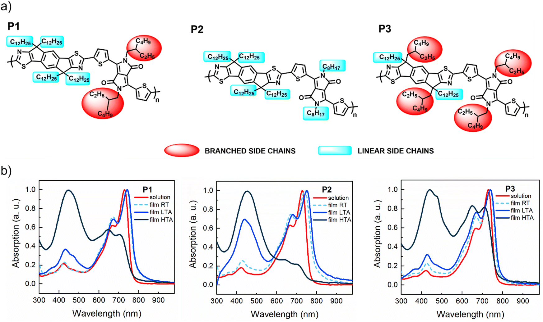 | ||
| Fig. 1 (a) Chemical structures of IDTz-DPP polymers, the branched and linear sidechains are highlighted in red and blue, respectively. (b) UV-vis absorption spectra of copolymers P1–P3 in chloroform solution, room temperature (RT) as casted films, low temperature annealed films (LTA = 110 °C) and high temperature annealed films (HTA = 270 °C) for 2 hours under argon atmosphere. | ||
In Fig. 1b we show the UV-vis absorption spectra of P1, P2 and P3 in chloroform solutions, along with the spectra of the freshly cast films and of films annealed at 110 °C and 270 °C. In solution, all copolymers show similar features: a π–π* transition around 430 nm and two distinct peaks at 670 nm and 730 nm, corresponding to 0–1 and 0–0 transitions, respectively. In thin films, these peaks redshift and the 670 nm band intensifies, indicating interchain π–π stacking. Low-temperature (110 °C) annealing further enhances the 670 nm band and 430 nm absorption, with P2 showing a fourfold increase in the 430 nm absorption, possibly due to the formation of a new conductive band. Annealing at 270 °C amplifies this band, which becomes dominant in all polymers, while the 670/730 nm bands nearly vanish for P2 and are reduced for P1 and P3. The evolution of the absorption spectra with annealing emphasizes the role of alkyl side chains in the structural re-organization of the films during thermal treatment.
The charge transport properties and bias stress stability have been evaluated using top-gate, bottom-contact OFETs,6 the device architecture is shown in Fig. 2a. To create n-type devices, the source/drain contacts have been modified with polyethyleneimine ethoxylated (PEIE),67 while pentafluorobenzenethiol (PFBT) was used for p-channel OFETs.68,69 The dielectric consisted of a bilayer of Cytop and parylene C subsequently deposited.16 Device transfer characteristics were measured by sweeping the VGS while keeping the VDS fixed at −60 V (for hole transport, left panel Fig. 2b) and 60 V (for electron transport, left panel Fig. 2c). The corresponding output curves for OFETs based on polymer P1 are depicted in the right panels of Fig. 2b and c, respectively. The charge carrier mobilities were determined to be μh = 0.3 cm2 V−1 s−1 (for hole transport), and μe = 1.3 cm2 V−1 s−1 (for electron transport). The I–V characteristics for the other two polymers are shown in Fig. S1 and S2 in the ESI,† along with the hysteresis data (Fig. S3, ESI†). At least 40 different OFETs of each type have been measured across multiple substrates and all devices that were considered for the analysis exhibited ideal or nearly ideal I–V characteristics.8,70 The non-zero intersection observed in the n-type output curves is likely attributed to the high contact resistance in these devices, as we will discuss later. Although the hole mobilities are relatively modest, the measured electron mobilities are on par with the best reported.22,23,30,31,35,36 To assess the impact of annealing temperature on charge carrier mobility, we fabricated four sets of samples for each polymer, maintaining a consistent device architecture, while varying the annealing temperatures. The maximum annealing temperature was chosen based on thermogravimetric analysis (TGA, Fig. S4, ESI†) and differential scanning calorimetry (DSC, Fig. S5, ESI†) to maximize performance without compromising material integrity. The dependence of device mobility on annealing temperature is presented in Fig. S6, ESI.† Based on this analysis, we have established optimal annealing protocol for each polymer. Results for 110 °C and the annealing temperature yielding the highest performance are presented in Fig. S7, ESI† and Table 1, demonstrating a clear enhancement in mobility upon annealing across all samples. Such response to thermal annealing is consistent with the results obtained on other polymers and was assigned to improved morphology of the semiconductor film, leading to reduced charge carrier trapping and lower contact resistance.71–73 P1 displayed the highest mobility under both low and high-temperature annealing conditions. The threefold improvement in mobility in films annealed at elevated temperatures suggests that the organization of alkyl groups plays a crucial role in establishing a favorable material morphology. Conversely, P2, which features exclusively straight dodecyl groups, exhibited an impressive eightfold improvement after high-temperature annealing. We hypothesize that while linear alkyl groups cannot yield an optimal configuration at moderate annealing temperatures, they can accommodate the alignment necessary for high performance when heated sufficiently. Polymer P3 demonstrated the smallest increase in mobility and the lowest final performance despite having the highest mass of the set. This observation may indicate that the presence of alkyl chains on both monomeric cores introduces excess entropic freedom, potentially disrupting electronic communication within the film. It also underscores the importance of reducing entropic freedom to optimize performance upon annealing.74,75
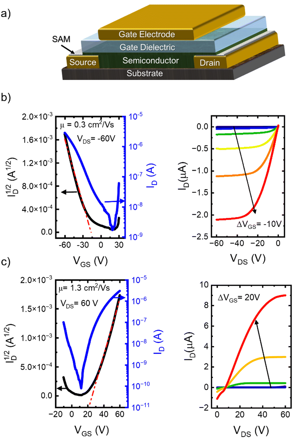 | ||
| Fig. 2 (a) Top gate, bottom contacts OFET geometry used in this study. (b) Transfer and output characteristics of a p-type OFET based on P1; here L/W = 40/400. (c) Transfer and output characteristics of an n-type OFET based on P1, here L/W = 100/400. | ||
| Annealing | Material | μ max (cm2 V−1 s−1) | μ avg (cm2 V−1 s−1) | ΔVth (V) | μ t/μ0 |
|---|---|---|---|---|---|
| LTA | P1 | 0.4 | 0.3 ± 0.04 | 1.2 | 0.9 |
| P2 | 0.1 | 0.05 ± 0.01 | 1.6 | 0.8 | |
| P3 | 0.2 | 0.1 ± 0.02 | 0.5 | 1.1 | |
| HTA | P1 | 1.3 | 1 ± 0.2 | 2.6 | 0.90 |
| P2 | 0.8 | 0.6 ± 0.1 | 1.9 | 1.02 | |
| P3 | 0.5 | 0.4 ± 0.1 | 1.5 | 1 | |
While the molecular structure of the polymer influences charge transport within the OFET channel, the efficiency of charge injection at the electrode–semiconductor interface is a critical factor determining mobility values (Table 1). Injection-limited transport often manifests as a dependence of mobility on device geometry; however, our data (Fig. S8 and S9, ESI†) reveals no clear trend. The work function of the Au electrode modified with PEIE (3.9 eV) lies significantly below the LUMO levels of all three polymers (P1![[thin space (1/6-em)]](https://www.rsc.org/images/entities/char_2009.gif) :3.51 eV, P2:3.38 eV, P3:3.37 eV, see Fig. S10, ESI†), suggesting the formation of a Schottky barrier at the interface. The height of this barrier influences charge injection efficiency and, consequently, the overall device mobility. To further investigate the relationship between charge injection and mobility, we conducted contact resistance analysis on our OFET devices using the gated Transmission Line Model (Fig. S11, ESI†).6,76 The results reveal a subtle correlation between contact resistance and mobility, with P1, the polymer with the highest mobility, exhibiting the lowest contact resistance. This suggests that while the molecular structure of P1 contributes to its superior charge transport properties, the lower contact resistance plays an important role.
:3.51 eV, P2:3.38 eV, P3:3.37 eV, see Fig. S10, ESI†), suggesting the formation of a Schottky barrier at the interface. The height of this barrier influences charge injection efficiency and, consequently, the overall device mobility. To further investigate the relationship between charge injection and mobility, we conducted contact resistance analysis on our OFET devices using the gated Transmission Line Model (Fig. S11, ESI†).6,76 The results reveal a subtle correlation between contact resistance and mobility, with P1, the polymer with the highest mobility, exhibiting the lowest contact resistance. This suggests that while the molecular structure of P1 contributes to its superior charge transport properties, the lower contact resistance plays an important role.
To understand the impact of film morphology on the electrical properties, we investigated the microstructure of the thin films using grazing-incidence wide-angle X-ray scattering (GIWAXS) measurements. Fig. 3 includes the 2D patterns images acquired on the films that have been annealed at 110 °C and the azimuthal integrations of these patterns can be found in Fig. S12 in the ESI.† Two weak, broad halos around q = 4 nm−1 (d ≈ 1.57 nm) and between 10–20 nm−1 (d ≈ 0.42 nm) can be seen, both features are likely associated with an amorphous, disordered structure. We identify, nevertheless, a hint of improved packing for the P3 sample, for which the peak at 14.5 nm−1 is slightly shifted towards high q (lower d), compared with the same peak for samples P1 and P2 (see Table 2).
 | ||
| Fig. 3 2D GIWAXS images patterns acquired on films of P1 (a), P2 (b) and P3 (c) annealed at low temperature (110 °C). | ||
| Material | q (nm−1) | d (nm) |
|---|---|---|
| P1 | 14.30 | 0.439 |
| P2 | 14.16 | 0.443 |
| P3 | 14.77 | 0.425 |
In addition, the former pattern presents a clear vertical scattering preference (highlighted with an arrow in Fig. 3), suggesting that the molecules are packed with a higher degree of order in a “face-on” configuration. Both effects, although subtle, indicate an improved packing mechanism for the sample P3, in comparison with the other two samples. The molecular orientation is critical for the performance of thin-film electronic devices. For example, in P(NDI2OD-T2) polymers, the horizontal electronic transfer in OFETs profits from a preferential “edge-on” orientation of the molecules.52 Although the exact impact of the disordered structure of IDT polymers on its electronic properties is not fully understood, the preferred vertical orientation of the π–π stacking (“face-on”) observed in the P3 sample after thermal annealing might be responsible for its lower mobility. Nevertheless, this difference, as with the orientation shift, is quite subtle. Corresponding 2D images of films annealed at temperatures ∼300 °C to replicate the conditions used for the device work are shown in Fig. S13, ESI,† together with their respective integrated profiles. These patterns do not show any remarkable difference compared to the ones associated to the low-temperature annealing. Overall, these results suggest that our films exhibit high electron mobilities despite lacking long-range order, similar to the recently reported amorphous donor–acceptor polymers, which displayed hole mobilities exceeding 1 cm2 V−1 s−1.9,56,77,78 The high mobilities of amorphous polymers stem from the rigid structure of the conjugated backbone and the resilience to the conformal fluctuations,66,79,80 although nanosized domains of the high order exist in these films.81 This behavior has primarily been observed in p-type polymers, with the highest previously reported mobility recorded for a near amorphous n-type polymer being μe = 0.34 cm2 V−1 s−1.78
The results presented so far certify the high-performance of our n-type polymer OFETs, with mobilities exceeding 1 cm2 V−1 s−1. Considering the limited prior work on the bias stress stability of such devices, our subsequent investigations will focus exclusively on the n-type devices. We conducted operational stability tests on all n-type OFETs. During these measurements, the transistors were kept under continuous operation (VGS = VDS = 60 V) for over 1000 min, with short interruptions at regular intervals to measure the transfer characteristics. Fig. 4a shows the evolution of the transfer characteristics measured in devices based on polymer P1 annealed at low temperatures, the results obtained on polymer P1 upon high temperature annealing, as well as on polymers P2 and P3 are included in Fig. S14–S16 (ESI†), while in Fig. S17 (ESI†) we plot the evolution of the drain current and subthreshold slope under bias stress. The changes recorded in the I–V curves are extremely small, in spite of the fact that these OFETs have been subjected to an aggressive bias stress protocol. To inspect these changes more carefully and quantitatively assess the device instabilities, we plotted the evolution of threshold voltage and charge carrier mobility as a function of bias stress time; the results are shown in Fig. 4b. These graphs correspond to average values obtained upon measuring multiple OFETs annealed at low temperature and the corresponding data obtained upon high temperature annealing is included in Fig. S18 (ESI†). Notably, the threshold voltage shift ΔVth is exceptionally low in all devices (ΔVth < 1.6 V), with values of ΔVth = 0.5 V being recorded in OFETs based on P3. Furthermore, the changes in mobilities are minimal. Several interesting observations from these results warrant further discussions. Firstly, the highest temperature needed during post-processing was 110 °C, making this technology compatible with flexible substrates. P3 exhibits the lowest charge carrier mobility, but the highest stability, suggesting that the optimal chemical structure of the polymer may differ when it comes to controlling these two properties. Secondly, it appears that the post-processing treatment for high mobility diverges from those yielding the highest stability. As such, the LTA devices were the most stable under bias stress degradation, despite having lower mobility compared to HTA films. While these conclusions are based on a limited data set, they provide the foundation for a more systematic and ample future study aimed at the development of polymer semiconductors that excel in both performance and stability.
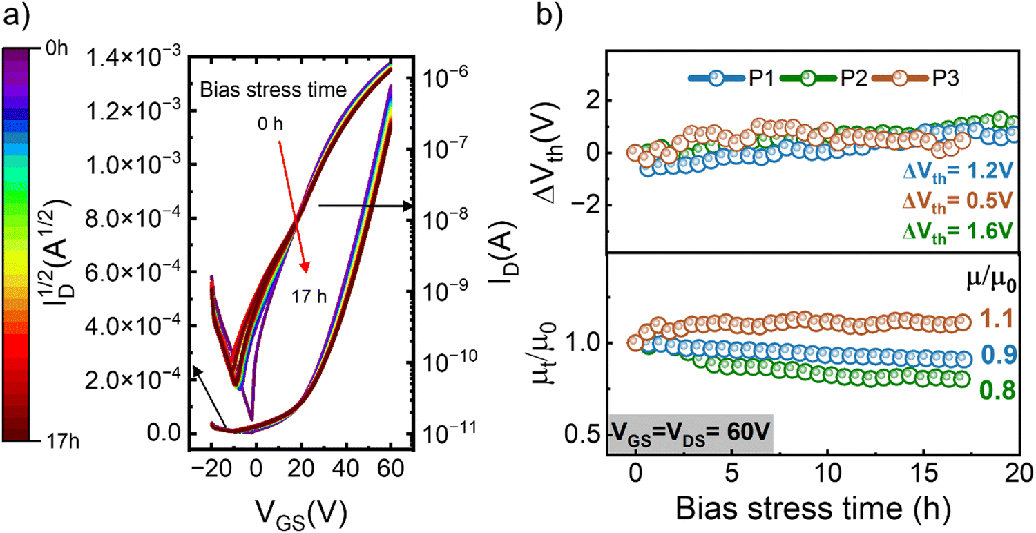 | ||
| Fig. 4 (a) Transfer curves measured on OFETs of P1 films annealed at low temperatures (LTA) during 17 h of continuous bias stress at VGS = VDS = 60 V. (b) Evolution of threshold voltage and mobility normalised to its value at t = 0 with time for n-type OFETs upon continuous bias stress at VGS = VDS = 60 V. | ||
The formation of electronic traps has been recognized as being the main reason for performance degradation in organic devices.16 To monitor the evolution of trap density during the operational stability tests, we analyzed the density of trap states (trap-DOS) using the Grünwald method.16,81–84Fig. 5a shows the trap DOS plotted as a function of energy E relative to the conduction band EC for each device type, and the two curves correspond to the trap-DOS spectrum before (black) and after (color) the application of bias stress for 1000 min. These graphs confirm the fact that the bias stress instabilities are a direct consequence of the generation of charge carrier traps upon bias stress. In Fig. 5b we include the schematic representation of the energetic and spatial distribution of trap states in the band gap of an organic semiconductor functioning in an n-channel OFET. Tail states near the band edges give rise to shallow, acceptor-like traps and deep trap states located within the band gap form a distinct peak. The peak is not apparent in our experimental results given the limited energy range accessible to us from transistor measurements. To quantitatively determine the density of the trap states created during bias stress, the difference between the two curves was evaluated for each polymer (yellow highlight). The density of traps increased by 2.6 × 10¹⁵ states per cm3 in P1, 2.5 × 10¹⁵ states per cm3 in P2, and 4.8 × 10¹⁴ states per cm3 in P3. These minimal changes in all polymers are in agreement with the small shifts in Vth and μ recorded in all samples and are partially due to the chosen device architecture, in which the dielectric layer also encapsulates the polymer films, limiting the diffusion of water and oxygen.16 Notably, the value of the density of traps generated in P3 is an order of magnitude lower than in P1 and P2, which explains its highest stability and suggests that the chemical composition of the polymers also plays a role in bias stress stability. While assessing the morphological evolution of the polymer films under bias stress could offer insights into the nature of trap formation (as seen in Fig. 5), our current top-gate device architecture precludes direct observation of the polymer layer post-stress. The overlying gate dielectric and electrode layers prevent access to the active material, limiting our ability to characterize any potential morphological changes induced by bias stress. Transitioning to a bottom-gate configuration would enable direct access to the polymer film, facilitating the analysis of such morphological changes. This approach could clarify the underlying mechanisms of degradation and potentially guide the development of strategies to mitigate these effects, thereby further enhancing device stability. Shelf-life stability tests have also been performed; the results are shown in Fig. S19 in the ESI.† The trends are consistent with those obtained in operational stability tests, where P3 is notably more stable compared to P1 and P2. Having demonstrated exceptional bias stress stability, the subsequent challenge lies in understanding the influence of mechanical strain on device performance.85–87 This is of paramount importance for the advancement of flexible electronics, as maintaining robust performance on curved surfaces and ensuring reproducibility in technologically relevant thin-film configurations represent crucial steps towards realizing their full potential.
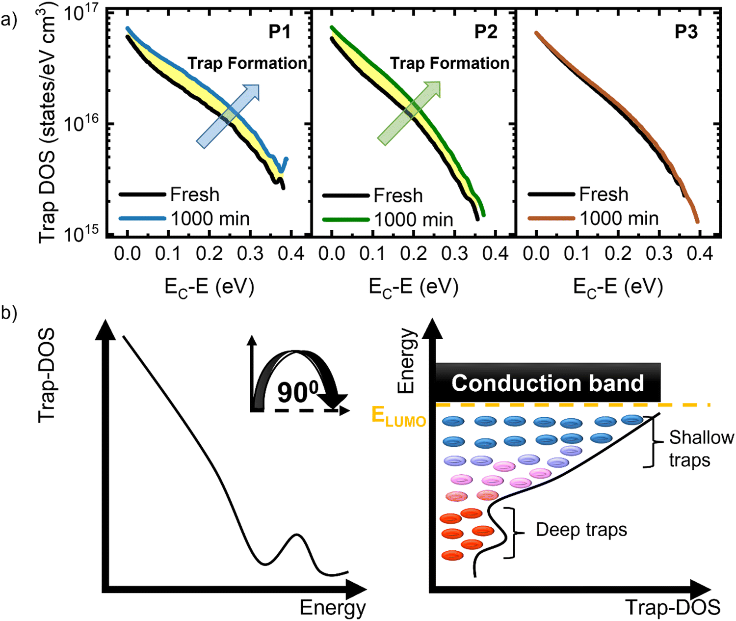 | ||
| Fig. 5 (a) Trap DOS spectra before and after bias stress in OFETs based on each of the three polymers. (b) (Left) Distribution of traps within the polymer bandgap: shallow traps are located near band edges (tail states) and deep traps form a distinct peak. (Right) Schematic representation of the spatial and energy diagram of trap-DOS consisting of acceptor-like shallow and deep traps. | ||
3. Conclusions
In summary, our study assessed the performance and stability of OFETs fabricated on donor–acceptor polymers incorporating IDTz and DPP units, alkylated with branched and/or linear side chains. Through tailored electrode surface modification, we tuned the charge transport from p to n-type, resulting in electron mobilities exceeding 1 cm2 V−1 s−1 in devices with near-ideal current–voltage characteristics. Remarkably, these devices exhibited minimal changes in mobilities, and exceptionally low threshold voltage shifts of 0.5 V were achieved under the application of bias stress at a constant 60 V for 1000 min in vacuum. Real-time monitoring of the trap density of states revealed that the degradation is caused by the formation of electronic trap states in the polymer bandgap and their density was proportional to the threshold voltage shift. Our findings indicate that a combination of linear and branched substituents is necessary for achieving high mobility. On the other hand, a high density of branched sidechains contributed to better stability, but negatively impacted charge carrier mobility. This suggests that the optimal polymer chemical structure for performance and stability may not align offering initial guidance for engineering materials that withstand bias stress. While this work provides valuable insights, establishing a comprehensive relationship between polymer structure, OFET design, and bias stress stability would require examining a larger dataset. Nevertheless, this study successfully addresses several key aspects necessary for developing a robust model linking these parameters, thus opening exciting avenues for future research in tailoring stable and high-performance organic electronics. The ultimate goal is to achieve both operational and environmental robustness. This requires addressing a multitude of factors that influence OFET stability, including material properties, device architecture, and environmental conditions. Our work serves as a significant step forward by decoupling these factors with focusing on operational stability under vacuum conditions. The exceptional bias stress resilience demonstrated by our n-type polymer OFETs reveals the potential of these polymers for operational stability. Further investigations into developing effective encapsulation strategies will be crucial to ensuring consistent performance in ambient conditions. Looking ahead, the high bias-stress stability demonstrated in our n-type polymer transistors represents a crucial step towards their incorporation into complex larger-scale organic integrated circuits.4. Experimental
Polymer synthesis
Starting materials were received from Sigma-Aldrich, Fisher Scientific or Alfa Aesar. Tetrakis(triphenylphosphine)palladium (Pd(PPh3)4, 99% (99.9+%-Pd)) was used as received from Strem Chemicals. All solvents were obtained from VWR and used without any further purification unless stated otherwise. IDTz monomers were synthesized according to previously reported procedures,60 while the DPP monomers were purchased from Solarmer. Flash chromatography on silica gel (pore size 60 Å, particle size 230–400 mesh) was used to purify the products, while Celite (Supleco R566) was used for filtration. Reactions were monitored by TLC on Merck Silica Gel 60 Å F-254 precoated plates (0.25 mm thickness), and components were visualized under 254 and 365 nm UV light. All the syntheses were performed using standard Schlenk techniques involving oven-dried glassware and Teflon coated stir bars under a dry argon atmosphere. Copolymers P1–P3 were synthesized using Stille coupling reaction. This involved reacting IDTz dibromides with stannylated DPP monomers in refluxing chlorobenzene, Pd(PPh3)4 was used as the catalyst, following the procedures described in Fig. S20, ESI.† Both monomers were used in 0.1 mmol amount with 5% mol Pd(PPh3)4 as the catalyst refluxing at 140 °C in 1 ml of dry chlorobenzene. All Stille polymerization reactions were performed using microwave type vials heated in aluminum blocks for 24 hours. The polymeric materials were precipitated into acidified methanol, then purified by soxhlet extraction for 24 hours with order of solvents: methanol, acetone, n-heptane. Last fractions of the polymers were washed with chloroform, concentrated, precipitated in methanol, filtered, and dried under high vacuum. Number-average molecular weights (Mn) and dispersities (Đ) of all copolymers were measured via size exclusion chromatography (SEC) in chlorobenzene using polystyrene as a standard (Fig. S21–S23, ESI†). Polymer molecular weights were determined using Agilent 1260 Infinity II high temperature GPC/SEC system (Agilent Technologies) using chlorobenzene as the eluent at 80 °C. Column set was calibrated with narrow polystyrene standards. The copolymers have Mn in the range of 40–65 kg mol−1 with Đ = 1.5–1.9, as summarized in Table S1 in the ESI.† NMR profiles are included in Fig. S24–S26, ESI.†Optical, electrochemical and thermal characterization
In Fig. S10, ESI† we show the cyclic voltammogram results along with the energy-level diagrams. The optical and electrochemical characteristics are included in Table S1, ESI.† TGA and DSC results are shown in Fig. S4 and S5 (ESI†), respectively.OFET fabrication and characterization
OFETs were fabricated on Si wafer substrates terminated with a 200 nm layer of thermally grown SiO2, diced into pieces of approximately 1.5 × 1.5 cm2. Prior to device fabrication, the substrates were cleaned in an acetone bath, then an isopropanol (IPA) bath, both at 85 °C. After drying under nitrogen, the substrates were exposed to UV-ozone treatment, then rinsed with deionized water to remove any residual organic matter, and dried again under nitrogen. Next, 3/40 nm of Ti/Au were deposited onto the clean substrates through a shadow mask to define the source and the drain electrodes. Channel lengths ranged from 30 μm to 100 μm, and channel widths ranged from 200 μm to 1000 μm. Multiple chips were measured for each fabrication condition. To create n-type devices a 0.05% solution of PEIE in 2-methoxyethanol was spin-coated onto the substrates with pre-defined contacts at a spinning speed of 5000 rpm for 60 seconds, followed by a rinse with a mild flow of deionized water. The sample was dried under N2 gas and then annealed at 110 °C for 10 min in a nitrogen environment. To fabricate p-type OFETs, the substrates were immersed in a solution of 20 μL of PFBT in 5 mL of high-purity ethanol for 30 min to allow self-assembly onto the contacts. After the treatment, the samples were rinsed with ethanol for 30 seconds and then dried with N2 gas. The polymers were spun-coated from a 5 mg mL−1 solution in room temperature chlorobenzene at 2000 rpm for 60 seconds. The resulting films have been annealed on a preheated hotplate for 10 min at 110 °C, 250 °C, 280 °C and 310 °C, respectively. To create the bilayer dielectric, a 1200 nm Cytop (CTL-809-M) was first spin-coated over the semiconducting polymer film at 2000 rpm for 60 seconds. The stack was then annealed on a hot plate at 110 °C for 25 min under nitrogen and placed in a vacuum desiccator overnight at room temperature. Next, a 300 nm parylene-C layer was deposited onto the Cytop layer in a custom-built reactor consisting of a quartz tube maintained at low pressure (10−2 torr) and divided into three distinct temperature zones. In the first section, the dimer di-para-xylene was heated at a temperature of 120 °C to sublime into dimeric gas, which was then passed into the second sector through a hot furnace where the temperature was maintained at 700 °C. The dimer then dissociated into its gaseous monomers inside the furnace. This resulted in monomeric gases polymerized onto the device placed in the third region of the tube maintained at room temperature forming a uniform conformal coating. The resulting bilayer dielectric has a final areal capacitance of Ci = 1.28 nF cm−2. Finally, a 40 nm layer of Au was thermally evaporated onto the device array through a shadow mask and served as a top gate electrode.Devices were electrically characterized using an Agilent 4155 Semiconductor Parameter Analyzer controlled by LabVIEW and/or SweepMe! Software (sweep-me.net). All measurements were performed in the dark and under vacuum (10−5 torr). The charge carrier mobility (μ) was determined from the slope of the square root of the drain current √IDversus the gate-source voltage VGS plot in the saturation regime.6 We ensured that the leakage current was at least two orders of magnitude lower than the drain current in all OFETs considered for analysis.
Stability tests on OFETs
Operational (bias–stress) stability tests were performed in vacuum (10−5 torr), in the dark, at room temperature. A continuous drain-source VDS and gate-source VGS voltage was applied for at least 1000 min at high voltages of VGS = VDS = 60 V and the saturation regime transistor characteristics were acquired at 30-minute intervals. At least 3 different devices of each type have been investigated and the results were found to be consistent. For the shelf-life tests, the saturation regime transfer characteristics (IDvs. VGS at VDS = +60 V) were recorded once a week for at least 10 weeks. After each measurement, the samples were stored in a vacuum with minimum exposure to light and ambient atmosphere.Grazing-incidence wide-angle X-ray scattering (GIWAXS) measurements
The GIWAXS experiments were carried out at ALBA Synchrotron (Barcelona, Spain), at NCD-SWEET scattering beamline. HTA and LTA polymer samples were prepared on PEIE treated silicon substrates, by using similar processing conditions as for OFET fabrication. We measured the sample in grazing-incidence geometry, projecting the X-ray beam on the thin film samples at an incident angle between 0.1° and 0.2°. The energy of the beam was set to 12.4 keV (λ = 0.1 nm) and the size of the beam to 50 μm × 50 μm. The samples were exposed to the beam for 5 seconds, and the patterns were collected with a LX255-HS (Rayonix) detector. Several frames were taken to increase the signal-to-noise ratio.Author contributions
The manuscript was written through contribution of all authors. All authors have given approval to the final version of the manuscript.Data availability
The data underlying the findings of this study are available upon reasonable request from the corresponding author. Any restrictions on data sharing will be due to ethical or privacy concerns.Conflicts of interest
The authors declare no conflict of interest.Acknowledgements
The work at Wake Forest University was supported by the National Science Foundation under grants ECCS-1810273 and DMR-2323423. M. A.-H. acknowledges support from the Qatar Research, Development and Innovation Council, Qatar National Research Fund (ARG01-0522-230270).References
- A. J. Boys, A. Carnicer-Lombarte, A. Güemes-Gonzalez, D. C. van Niekerk, S. Hilton, D. G. Barone, C. M. Proctor, R. M. Owens and G. G. Malliaras, Adv. Mater., 2023, 35, 2207847 CrossRef CAS PubMed.
- G. Zhang, F. R. Lin, F. Qi, T. Heumüller, A. Distler, H.-J. Egelhaaf, N. Li, P. C. Y. Chow, C. J. Brabec, A. K.-Y. Jen and H.-L. Yip, Chem. Rev., 2022, 122, 14180 CrossRef CAS.
- I. McCulloch, M. Chabinyc, C. Brabec, C. B. Nielsen and S. E. Watkins, Nat. Mater., 2023, 22, 1304 CrossRef CAS PubMed.
- F. Torricelli, D. Z. Adrahtas, Z. Bao, M. Berggren, F. Biscarini, A. Bonfiglio, C. A. Bortolotti, C. D. Frisbie, E. Macchia, G. G. Malliaras, I. McCulloch, M. Moser, T.-Q. Nguyen, R. M. Owens, A. Salleo, A. Spanu and L. Torsi, Nat. Rev. Methods Primers, 2021, 1, 1 CrossRef.
- S. Fratini, M. Nikolka, A. Salleo, G. Schweicher and H. Sirringhaus, Nat. Mater., 2020, 19, 491 CrossRef CAS PubMed.
- Z. A. Lamport, H. F. Haneef, S. Anand, M. Waldrip and O. D. Jurchescu, J. Appl. Phys., 2018, 124, 071101 CrossRef.
- H. Klauk, Chem. Soc. Rev., 2010, 39, 2643 RSC.
- H. H. Choi, K. Cho, C. D. Frisbie, H. Sirringhaus and V. Podzorov, Nat. Mater., 2018, 17, 2 CrossRef CAS PubMed.
- Z. A. Lamport, K. J. Barth, H. Lee, E. Gann, S. Engmann, H. Chen, M. Guthold, I. McCulloch, J. E. Anthony, L. J. Richter, D. M. DeLongchamp and O. D. Jurchescu, Nat. Commun., 2018, 9, 5130 CrossRef PubMed.
- G. Kim, S.-J. Kang, G. K. Dutta, Y.-K. Han, T. J. Shin, Y.-Y. Noh and C. Yang, J. Am. Chem. Soc., 2014, 136, 9477 CrossRef CAS PubMed.
- A. F. Paterson, N. D. Treat, W. Zhang, Z. Fei, G. Wyatt-Moon, H. Faber, G. Vourlias, P. A. Patsalas, O. Solomeshch, N. Tessler, M. Heeney and T. D. Anthopoulos, Adv. Mater., 2016, 28, 7791 CrossRef CAS PubMed.
- H. Li, B. C.-K. Tee, J. J. Cha, Y. Cui, J. W. Chung, S. Y. Lee and Z. Bao, J. Am. Chem. Soc., 2012, 134, 2760 CrossRef CAS PubMed.
- X. Xu, Y. Yao, B. Shan, X. Gu, D. Liu, J. Liu, J. Xu, N. Zhao, W. Hu and Q. Miao, Adv. Mater., 2016, 28, 5276 CrossRef CAS PubMed.
- J. Chen, W. Zhang, L. Wang and G. Yu, Adv. Mater., 2023, 35, 2210772 CrossRef CAS PubMed.
- M. Chu, J.-X. Fan, S. Yang, D. Liu, C. F. Ng, H. Dong, A.-M. Ren and Q. Miao, Adv. Mater., 2018, 30, 1803467 CrossRef PubMed.
- H. F. Iqbal, Q. Ai, K. J. Thorley, H. Chen, I. McCulloch, C. Risko, J. E. Anthony and O. D. Jurchescu, Nat. Commun., 2021, 12, 2352 CrossRef CAS.
- S. Ando, R. Murakami, J. Nishida, H. Tada, Y. Inoue, S. Tokito and Y. Yamashita, J. Am. Chem. Soc., 2005, 127, 14996 CrossRef CAS PubMed.
- X. Tao, W. Li, Q. Wu, H. Wei, Y. Yan, L. Zhao, Y. Hu, Y. Zhao, H. Chen and Y. Liu, Adv. Funct. Mater., 2023, 33, 2210846 CrossRef CAS.
- R. Kim, P. S. K. Amegadze, I. Kang, H.-J. Yun, Y.-Y. Noh, S.-K. Kwon and Y.-H. Kim, Adv. Funct. Mater., 2013, 23, 5719 CrossRef CAS.
- T. Lei, J.-H. Dou, X.-Y. Cao, J.-Y. Wang and J. Pei, J. Am. Chem. Soc., 2013, 135, 12168 CrossRef CAS PubMed.
- S. Nam, D. Khim, G. T. Martinez, A. Varambhia, P. D. Nellist, Y. Kim, T. D. Anthopoulos and D. D. C. Bradley, Adv. Mater., 2021, 33, 2100421 CrossRef CAS PubMed.
- T. Okamoto, S. Kumagai, E. Fukuzaki, H. Ishii, G. Watanabe, N. Niitsu, T. Annaka, M. Yamagishi, Y. Tani, H. Sugiura, T. Watanabe, S. Watanabe and J. Takeya, Sci. Adv., 2020, 6, eaaz0632 CrossRef CAS.
- H. Yan, Z. Chen, Y. Zheng, C. Newman, J. R. Quinn, F. Dötz, M. Kastler and A. Facchetti, Nature, 2009, 457, 679 CrossRef CAS PubMed.
- Z. Fei, Y. Han, J. Martin, F. H. Scholes, M. Al-Hashimi, S. Y. AlQaradawi, N. Stingelin, T. D. Anthopoulos and M. Heeney, Macromolecules, 2016, 49, 6384 CrossRef CAS.
- S. Brixi, O. A. Melville, B. Mirka, Y. He, A. D. Hendsbee, H. Meng, Y. Li and B. H. Lessard, Sci. Rep., 2020, 10, 4014 CrossRef CAS PubMed.
- Y. Han, Y. Liu, J. Yuan, H. Dong, Y. Li, W. Ma, S.-T. Lee and B. Sun, ACS Nano, 2017, 11, 7215 CrossRef CAS PubMed.
- X. Guo, F. S. Kim, M. J. Seger, S. A. Jenekhe and M. D. Watson, Chem. Mater., 2012, 24, 1434 CrossRef CAS.
- Z. Wu, C. Sun, S. Dong, X.-F. Jiang, S. Wu, H. Wu, H.-L. Yip, F. Huang and Y. Cao, J. Am. Chem. Soc., 2016, 138, 2004 CrossRef CAS PubMed.
- Y. He, X. Li, H. Liu, H. Meng, G. Ying Wang, B. Cui, J. Wang and Y. Li, J. Mater. Chem. C, 2018, 6, 1349 RSC.
- C. Kanimozhi, N. Yaacobi-Gross, K. W. Chou, A. Amassian, T. D. Anthopoulos and S. Patil, J. Am. Chem. Soc., 2012, 134, 16532 CrossRef CAS PubMed.
- J. H. Park, E. H. Jung, J. W. Jung and W. H. Jo, Adv. Mater., 2013, 25, 2583 CrossRef CAS PubMed.
- Q. Liu, S. E. Bottle and P. Sonar, Adv. Mater., 2020, 32, 1903882 CrossRef CAS PubMed.
- W. S. Yoon, S. K. Park, I. Cho, J.-A. Oh, J. H. Kim and S. Y. Park, Adv. Funct. Mater., 2013, 23, 3519 CrossRef CAS.
- K. Guo, J. Bai, Y. Jiang, Z. Wang, Y. Sui, Y. Deng, Y. Han, H. Tian and Y. Geng, Adv. Funct. Mater., 2018, 28, 1801097 CrossRef.
- T. Lei, J.-H. Dou, Z.-J. Ma, C.-J. Liu, J.-Y. Wang and J. Pei, Chem. Sci., 2013, 4, 2447 RSC.
- T. Lei, J.-H. Dou, X.-Y. Cao, J.-Y. Wang and J. Pei, Adv. Mater., 2013, 25, 6589 CrossRef CAS PubMed.
- Y. He, C. Guo, B. Sun, J. Quinn and Y. Li, Polym. Chem., 2015, 6, 6689 RSC.
- Y. He, J. T. E. Quinn, D. Hou, J. H. L. Ngai and Y. Li, J. Mater. Chem. C, 2017, 5, 12163 RSC.
- Z. Yan, B. Sun and Y. Li, Chem. Commun., 2013, 49, 3790 RSC.
- T. Lei, X. Xia, J.-Y. Wang, C.-J. Liu and J. Pei, J. Am. Chem. Soc., 2014, 136, 2135 CrossRef CAS PubMed.
- A.-R. Han, J. Lee, H. R. Lee, J. Lee, S.-H. Kang, H. Ahn, T. J. Shin, J. H. Oh and C. Yang, Macromolecules, 2016, 49, 3739 CrossRef CAS.
- E. K. Lee, M. Y. Lee, C. H. Park, H. R. Lee and J. H. Oh, Adv. Mater., 2017, 29, 1703638 CrossRef.
- Z. Zhao, Z. Yin, H. Chen, Y. Guo, Q. Tang and Y. Liu, J. Mater. Chem. C, 2017, 5, 2892 RSC.
- K. Iijima, Y. L. Gal, T. Higashino, D. Lorcy and T. Mori, J. Mater. Chem. C, 2017, 5, 9121 RSC.
- P. A. Bobbert, A. Sharma, S. G. J. Mathijssen, M. Kemerink and D. M. de Leeuw, Adv. Mater., 2012, 24, 1146 CrossRef CAS PubMed.
- H. Sirringhaus, Adv. Mater., 2009, 21, 3859 CrossRef CAS.
- M. Barra, F. V. Di Girolamo, N. A. Minder, I. Gutiérrez Lezama, Z. Chen, A. Facchetti, A. F. Morpurgo and A. Cassinese, Appl. Phys. Lett., 2012, 100, 133301 CrossRef.
- M. Stolte, M. Gsänger, R. Hofmockel, S.-L. Suraru and F. Würthner, Phys. Chem. Chem. Phys., 2012, 14, 14181 RSC.
- Y. Fujisaki, Y. Nakajima, D. Kumaki, T. Yamamoto, S. Tokito, T. Kono, J. Nishida and Y. Yamashita, Appl. Phys. Lett., 2010, 97, 133303 CrossRef.
- A. D. Scaccabarozzi, J. I. Basham, L. Yu, P. Westacott, W. Zhang, A. Amassian, I. McCulloch, M. Caironi, D. J. Gundlach and N. Stingelin, J. Mater. Chem. C, 2020, 8, 15406 RSC.
- D. X. Long, E.-Y. Choi and Y.-Y. Noh, Dyes Pigm., 2017, 142, 323 CrossRef CAS.
- D. Simatos, L. J. Spalek, U. Kraft, M. Nikolka, X. Jiao, C. R. McNeill, D. Venkateshvaran and H. Sirringhaus, APL, Materials, 2021, 9, 041113 CAS.
- Q. Chen, R. Zhu, X. Zhao, B. Hao, B. Li, Z. Yu, H. Sun, J. Wu, C. L. Tan and Y. Xu, Appl. Phys. Lett., 2022, 121, 243302 CrossRef CAS.
- Z. Yi, S. Wang and Y. Liu, Adv. Mater., 2015, 27, 3589 CrossRef CAS PubMed.
- B. Sun, W. Hong, Z. Yan, H. Aziz and Y. Li, Adv. Mater., 2014, 26, 2636 CrossRef CAS PubMed.
- W. Zhang, J. Smith, S. E. Watkins, R. Gysel, M. McGehee, A. Salleo, J. Kirkpatrick, S. Ashraf, T. Anthopoulos, M. Heeney and I. McCulloch, J. Am. Chem. Soc., 2010, 132, 11437 CrossRef CAS PubMed.
- H. Bronstein, D. S. Leem, R. Hamilton, P. Woebkenberg, S. King, W. Zhang, R. S. Ashraf, M. Heeney, T. D. Anthopoulos, J. de Mello and I. McCulloch, Macromolecules, 2011, 44, 6649 Search PubMed.
- Y. Lin, Q. He, F. Zhao, L. Huo, J. Mai, X. Lu, C.-J. Su, T. Li, J. Wang, J. Zhu, Y. Sun, C. Wang and X. Zhan, J. Am. Chem. Soc., 2016, 138, 2973 CrossRef CAS PubMed.
- M. Nikolka, M. Hurhangee, A. Sadhanala, H. Chen, I. McCulloch and H. Sirringhaus, Adv. Electron. Mater., 2018, 4, 1700410 CrossRef.
- M. Barłóg, X. Zhang, I. Kulai, D. S. Yang, D. N. Sredojevic, A. Sil, X. Ji, K. S. M. Salih, H. S. Bazzi, H. Bronstein, L. Fang, J. Kim, T. J. Marks, X. Guo and M. Al-Hashimi, Chem. Mater., 2019, 31, 9488 Search PubMed.
- E. Zaborova, P. Chávez, R. Bechara, P. Lévêque, T. Heiser, S. Méry and N. Leclerc, Chem. Commun., 2013, 49, 9938 RSC.
- T. Lei, J.-H. Dou and J. Pei, Adv. Mater., 2012, 24, 6457 Search PubMed.
- B. C. Schroeder, T. Kurosawa, T. Fu, Y.-C. Chiu, J. Mun, G.-J. N. Wang, X. Gu, L. Shaw, J. W. E. Kneller, T. Kreouzis, M. F. Toney and Z. Bao, Adv. Funct. Mater., 2017, 27, 1701973 Search PubMed.
- N. Luo, P. Ren, Y. Feng, X. Shao, H.-L. Zhang and Z. Liu, J. Phys. Chem. Lett., 2022, 13, 1131 CrossRef CAS PubMed.
- M. Pei, J.-H. Kim, S. On, H.-K. Lee, K. Cho, D.-H. Hwang and H. Yang, Macromol. Chem. Phys., 2017, 218, 1700135 CrossRef.
- A. Wadsworth, H. Chen, K. J. Thorley, C. Cendra, M. Nikolka, H. Bristow, M. Moser, A. Salleo, T. D. Anthopoulos, H. Sirringhaus and I. McCulloch, J. Am. Chem. Soc., 2020, 142, 652 Search PubMed.
- Y. Zhou, C. Fuentes-Hernandez, J. Shim, J. Meyer, A. J. Giordano, H. Li, P. Winget, T. Papadopoulos, H. Cheun, J. Kim, M. Fenoll, A. Dindar, W. Haske, E. Najafabadi, T. M. Khan, H. Sojoudi, S. Barlow, S. Graham, J.-L. Brédas, S. R. Marder, A. Kahn and B. Kippelen, Science, 2012, 336, 327 CrossRef CAS PubMed.
- J. W. Ward, M. A. Loth, R. J. Kline, M. Coll, C. Ocal, J. E. Anthony and O. D. Jurchescu, J. Mater. Chem., 2012, 22, 19047 RSC.
- Y. Mei, D. Fogel, J. Chen, J. W. Ward, M. M. Payne, J. E. Anthony and O. D. Jurchescu, Org. Electron., 2017, 50, 100 CrossRef CAS.
- E. G. Bittle, J. I. Basham, T. N. Jackson, O. D. Jurchescu and D. J. Gundlach, Nat. Commun., 2016, 7, 10908 CrossRef CAS PubMed.
- J. S. Lee, S. K. Son, S. Song, H. Kim, D. R. Lee, K. Kim, M. J. Ko, D. H. Choi, B. Kim and J. H. Cho, Chem. Mater., 2012, 24, 1316 CrossRef CAS.
- Z. Chen, M. J. Lee, R. Shahid Ashraf, Y. Gu, S. Albert-Seifried, M. Meedom Nielsen, B. Schroeder, T. D. Anthopoulos, M. Heeney, I. McCulloch and H. Sirringhaus, Adv. Mater., 2012, 24, 647 Search PubMed.
- C. B. Nielsen, M. Turbiez and I. McCulloch, Adv. Mater., 2013, 25, 1859 CrossRef CAS PubMed.
- J. Mei and Z. Bao, Chem. Mater., 2014, 26, 604 CrossRef CAS.
- Z. Qian, L. Galuska, W. W. McNutt, M. U. Ocheje, Y. He, Z. Cao, S. Zhang, J. Xu, K. Hong, R. B. Goodman, S. Rondeau-Gagné, J. Mei and X. Gu, J. Polym. Sci., Part B: Polym. Phys., 2019, 57, 1635 CrossRef CAS.
- M. Waldrip, O. D. Jurchescu, D. J. Gundlach and E. G. Bittle, Adv. Funct. Mater., 2020, 30, 1904576 Search PubMed.
- X. Zhang, H. Bronstein, A. J. Kronemeijer, J. Smith, Y. Kim, R. J. Kline, L. J. Richter, T. D. Anthopoulos, H. Sirringhaus, K. Song, M. Heeney, W. Zhang, I. McCulloch and D. M. DeLongchamp, Nat. Commun., 2013, 4, 2238 CrossRef PubMed.
- X. Cao, H. Li, J. Hu, H. Tian, Y. Han, B. Meng, J. Liu and L. Wang, Angew. Chem., Int. Ed., 2023, 62, e202212979 Search PubMed.
- D. Venkateshvaran, M. Nikolka, A. Sadhanala, V. Lemaur, M. Zelazny, M. Kepa, M. Hurhangee, A. J. Kronemeijer, V. Pecunia, I. Nasrallah, I. Romanov, K. Broch, I. McCulloch, D. Emin, Y. Olivier, J. Cornil, D. Beljonne and H. Sirringhaus, Nature, 2014, 515, 384 Search PubMed.
- C. Cendra, L. Balhorn, W. Zhang, K. O’Hara, K. Bruening, C. J. Tassone, H.-G. Steinrück, M. Liang, M. F. Toney, I. McCulloch, M. L. Chabinyc, A. Salleo and C. J. Takacs, ACS Macro Lett., 2021, 10, 1306 Search PubMed.
- I. Dobryden, V. V. Korolkov, V. Lemaur, M. Waldrip, H.-I. Un, D. Simatos, L. J. Spalek, O. D. Jurchescu, Y. Olivier, P. M. Claesson and D. Venkateshvaran, Nat. Commun., 2022, 13, 3076 Search PubMed.
- K. P. Goetz, H. F. Iqbal, E. G. Bittle, C. A. Hacker, S. Pookpanratana and O. D. Jurchescu, Mater. Horiz., 2022, 9, 271 RSC.
- H. F. Iqbal, E. K. Holland, J. E. Anthony and O. D. Jurchescu, Mater. Horiz., 2020, 7, 2390 RSC.
- P. J. Diemer, Z. A. Lamport, Y. Mei, J. W. Ward, K. P. Goetz, W. Li, M. M. Payne, M. Guthold, J. E. Anthony and O. D. Jurchescu, Appl. Phys. Lett., 2015, 107, 103303 CrossRef.
- T. Kubo, R. Häusermann, J. Tsurumi, J. Soeda, Y. Okada, Y. Yamashita, N. Akamatsu, A. Shishido, C. Mitsui, T. Okamoto, S. Yanagisawa, H. Matsui and J. Takeya, Nat. Commun., 2016, 7, 11156 CrossRef CAS PubMed.
- H. H. Choi, H. T. Yi, J. Tsurumi, J. J. Kim, A. L. Briseno, S. Watanabe, J. Takeya, K. Cho and V. Podzorov, Adv. Sci., 2020, 7, 1901824 CrossRef CAS PubMed.
- A. M. Zeidell, D. S. Filston, M. Waldrip, H. F. Iqbal, H. Chen, I. McCulloch and O. D. Jurchescu, Adv. Mater. Technol., 2020, 5, 2000390 CrossRef CAS.
Footnotes |
| † Electronic supplementary information (ESI) available. See DOI: https://doi.org/10.1039/d4tc03294b |
| ‡ M. M. and M. B. contributed equally to this work. |
| This journal is © The Royal Society of Chemistry 2024 |