 Open Access Article
Dy-Doped BiFeO3 thin films: piezoelectric and bandgap tuning†
Quentin
Micard‡
a,
Samuel
Margueron
b,
Ausrine
Bartasyte
b,
Guglielmo G.
Condorelli
 a and
Graziella
Malandrino
 *a
*a
aDipartimento di Scienze Chimiche, Università di Catania, and INSTM UdR Catania, Viale A. Doria 6, I-95125 Catania, Italy. E-mail: gmalandrino@unict.it
bFEMTO-ST Institute, University of Bourgogne Franche-Comté CNRS UMR 6174, 26 Rue de l’Epitaphe, F-25030 Besançon, France
First published on 24th February 2022
Abstract
Multiferroic materials, including lead-free BiFeO3, are of special interest for their challenging functional properties which can suit various applications. This paper reports the optimization of the MOCVD process used for the deposition of epitaxial thin films of Dy-doped bismuth ferrite, Bi(1−x)DyxFeO3 (with 0 ≤ x ≤ 0.11), on conductive SrTiO3:Nb(100) single crystal substrates. The tri-metallic precursor mixture thermal behaviour is assessed under working conditions up to 130 °C and the impact of Dy-doping on the film morphology (FE-SEM), growth rate and structure (XRD and Raman spectroscopy) is systematically reported and compared to the literature. For Dy-doping with x ≤ 0.11, no change of symmetry has been observed and all films show great homogeneity. Piezoresponse force microscopy (PFM) and piezoresponse force spectroscopy (PFS) have been applied to investigate the ferroelectric and piezoelectric properties of BiFeO3 and Bi(1−x)DyxFeO3 films. Ferroelectric and piezoelectric responses are good up to a Dy-doping of 0.08 with a significant reduction of the optical bandgap: 2.25 eV (for the highest doping at x = 0.11) compared to 2.68 eV of pure BiFeO3 films.
Introduction
Among multiferroic materials, BiFeO3 (BFO) and its derived systems have been extensively investigated.1 The presence of at least two ferroic orders gives fundamental physical properties that attract lots of attention for potential applications in several fields such as signal transduction, sensors, memory devices and spintronics.2 Moreover, with its high ferroelectric and magnetic transition temperatures (TC = 1103 K and TN = 643 K) BFO can maintain good performance in a high temperature environment. Recently, BFO has been investigated as a potential material for energy harvesting. Its piezoelectric, pyroelectric and photovoltaic properties make it highly versatile for the creation of a hybrid energy harvester.3,4 With other lead-free perovskite-like materials, LiNbO3 or (K,Na)NbO3, it is one of the important candidates to replace Pb(ZrxTi1−x)O3 (PZT), which, despite its good performance and broad application for piezoelectric actuators, has a high environmental impact.5–7BFO offers a high intrinsic polarization with 60 μC cm−2 along [001]pc (pc stands for the pseudocubic unit cell)1 and a relatively low bandgap of around 2.7 eV. These characteristics make it a perfect candidate as a lead-free material with appealing ferroelectric, piezoelectric and photovoltaic properties. Nevertheless, BFO suffers several critical flaws which limit its integration into a functional device. The major problem remains the presence of a leaky behaviour. Among all the approaches used to optimize BFO properties, the control of film stress or post process treatment and single or co-doping at the A/B sites are the most established methods to tune BFO properties, reduce the leakage current and increase the ferroelectric properties.8–14 Substituting Bi3+ ions located at the A-site of the BFO perovskite cell with rare-earth (RE) elements has been extensively studied for powders, ceramics and films.15,16 Not only material properties are impacted by doping, but also changes in the material structure can be observed for increased concentration of dopants. In the case of RE element doping, a phase transition from pseudocubic (specifically a trigonal system with a R3C space group) to orthorhombic is often observed and the dopant percentage leading to a phase transition varies depending on the element nature and the preparation method.16 Among RE elements, Dy-doping has attracted considerable attention, since its effect has not been deeply investigated, but a few known reports have pointed to interesting results on magnetoelectric and pyroelectric properties.17–19 Phase transition in a single-phase solid solution does not always occur in highly doped systems and, instead, the formation of nanocomposites with the presence of at least two separate phases can be achieved. One of the most studied systems among these nanocomposites is the BiFeO3–BaTiO3 mixture.20–23
The presence of an increased number of elements makes the deposition process complex, where temperature, vaporization rate and final stoichiometry are essential parameters. Doped and undoped BFO films have already been obtained using many different deposition routes. High quality films have been deposited by pulsed laser deposition (PLD),24–27 but most of the time chemical solution deposition,27,28 sputtering29,30 and sol–gel processes31,32 have been used.
Metal–organic chemical vapor deposition (MOCVD) has been less investigated for the deposition of BFO films,33–36 despite being very appealing with regard to homogeneous deposition on large substrates, easy up-scaling possibility, and a large choice of available substrates and precursors.
This paper presents the doping at the A-site of BiFeO3 thin films with dysprosium and the optimization of the MOCVD process. (Bi1−x,Dyx)FeO3 (BDFO with 0 ≤ x ≤ 0.11) systems have been prepared on SrTiO3(100) (from now on STO) and conductive SrTiO3:Nb(100) (from now on STO:Nb) single crystal substrates. In this study, we confirm the ferroelectric/bandgap/piezoelectric tunability of the BFO phase films by using dysprosium doping. A tri-metallic mixture composed of Bi(phenyl)3, Fe(tmhd)3 and Dy(hfa)3·diglyme [phenyl = –C6H5; H-tmhd = 2,2,6,6-tetramethyl-3,5-heptandione; H-hfa = 1,1,1,5,5,5-hexafluoro-2,4-pentanedione; diglyme = bis(2-methoxyethyl)ether] has been prepared and used as a single source precursor. Its thermal stability and volatility have been confirmed by thermogravimetric analysis (TGA). Film surface, homogeneous morphology and chemical composition have been investigated through FE-SEM coupled with EDX, confirming and quantifying Dy doping in the deposited films. The epitaxial growth of BFO and BDFO films on single crystal STO substrates has been assessed by X-ray diffraction analysis. Film quality and structure have also been investigated by Raman spectroscopy and the Dy-doping impact on optical bandgap materials has also been evaluated. Finally, the relationship between the Dy doping percentage and sample ferroelectric and piezoelectric responses has been assessed by piezoresponse force microscopy (PFM) and local piezoresponse force spectroscopy (PFS).
Experimental section
Film depositions were performed in a customized horizontal, hot-wall MOCVD reactor. Bi(phenyl)3 and Fe(tmhd)3 precursors were purchased from Strem Chemicals Inc. and were used without further purification, while Dy(hfa)3·diglyme was synthesized in our lab following a protocol similar to that reported in ref. 37. A tri-metallic mixture of Bi(phenyl)3, Fe(tmhd)3 and Dy(hfa)3·diglyme was placed in an alumina boat and heated at 120 °C. The reactant and carrier gases were oxygen and argon, respectively, and their flows were kept constant for the whole deposition at 150 sccm (standard cubic centimeter per minute). The depositions were carried out in the temperature range from 750 °C to 800 °C for 1 hour. BFO films were deposited on a 5 mm × 10 mm STO:Nb(100) substrate acting, at the same time, as the bottom electrode for ferroelectric and functional characterization.38XRD patterns were recorded using a Rigaku Smartlab diffractometer, equipped with a rotating anode of Cu Kα radiation operating at 45 kV and 200 mA. Bragg–Brentano patterns were acquired with a resolution step of 0.02°. The in-plane diffraction pattern was recorded with an incidence angle (ω) of 0.5°. The film surface morphology was examined by field emission scanning electron microscopy (FE-SEM) using a ZEISS VP 55 microscope. The film atomic composition was analysed by energy dispersive X-ray analysis (EDX), using an INCA Oxford windowless detector with an electron beam energy of 15 keV and a resolution of 127 eV for Mn Kα.
Raman spectra were recorded using a S&l Monovista high-resolution micro-Raman spectrometer. Raman spectroscopy measurements were performed in backscattering geometry with a 100x magnification objective (1 μm focusing spot) at room temperature. We used a 532 nm laser, and its power was maintained at around 1 mW to avoid heating the sample. Incident laser and scattering light have been polarized parallel −Z(XX)Z or perpendicular to each other −Z(XY)Z.
X-Ray photoelectron spectroscopy (XPS) measurements were performed using a PHI 5000 versa probe II equipped with an electron beam excited monochromated Al Kα source (beam size/power 150 μm/15 W). Depth profiles were obtained by alternating Ar ion sputter operating at 2 kV on 3 × 3 mm2 area and XPS analysis in the centre of the crater.
The absorption spectra of films deposited on colourless and transparent STO(100) substrate were collected using a Jasco V-650 spectrophotometer. Then, the bandgap was calculated by using Tauc plot equation.
Scanning probe microscopy and spectroscopy were performed using a Solver P47 NT-MTD instrument. For the simultaneous evaluation of topographic and piezoelectric properties, atomic force and piezoresponce force microscopies (AFM and PFM) were performed by adopting the Au-coated silicon probe with a nominal 35 nm tip curvature radius and a typical force constant of 0.1 N. AFM images were obtained in a contact mode. The noise level before and after each measurement was 0.01 nm.
Results and discussion
A simple MOCVD route, using a solid multicomponent precursor mixture, has been applied for the deposition of pure and Dy-doped BiFeO3 films. For Bi, Fe and Dy sources, Bi(phenyl)3, Fe(tmhd)3, and Dy(hfa)3·diglyme have been used to deposit pure BFO and to dope BFO films at the A-site with Dy3+. Precursor mixtures with different Dy concentrations have been prepared for the deposition of the doped films (using Dy/(Dy + Bi) molar ratios of 8%, 11% and 15%). The three corresponding doping levels in the films, evaluated through EDX, are reported here as: Bi0.94Dy0.06FeO3 (from now on BDFO-6%), Bi0.92Dy0.08FeO3 (BDFO-8%) and Bi0.89Dy0.11FeO3 (BDFO-11%).The thermal behaviours of the multicomponent source containing Bi(phenyl)3, Fe(tmhd)3, and Dy(hfa)3·diglyme have been investigated by thermogravimetric (TG) measurements at atmospheric pressure under a nitrogen flow. A precedent study has shown that the Bi(phenyl)3/Fe(tmhd)3 mixture in a 1![[thin space (1/6-em)]](https://www.rsc.org/images/entities/char_2009.gif) :
:![[thin space (1/6-em)]](https://www.rsc.org/images/entities/char_2009.gif) 0.66 ratio has an excellent thermal behaviour with a final residue of 5%.39 To focus on the thermal study of the three metallic precursor mixtures, the higher content Dy mixture in a ratio Bi
0.66 ratio has an excellent thermal behaviour with a final residue of 5%.39 To focus on the thermal study of the three metallic precursor mixtures, the higher content Dy mixture in a ratio Bi![[thin space (1/6-em)]](https://www.rsc.org/images/entities/char_2009.gif) :
:![[thin space (1/6-em)]](https://www.rsc.org/images/entities/char_2009.gif) Fe
Fe![[thin space (1/6-em)]](https://www.rsc.org/images/entities/char_2009.gif) :
:![[thin space (1/6-em)]](https://www.rsc.org/images/entities/char_2009.gif) Dy of 1
Dy of 1![[thin space (1/6-em)]](https://www.rsc.org/images/entities/char_2009.gif) :
:![[thin space (1/6-em)]](https://www.rsc.org/images/entities/char_2009.gif) 0.66
0.66![[thin space (1/6-em)]](https://www.rsc.org/images/entities/char_2009.gif) :
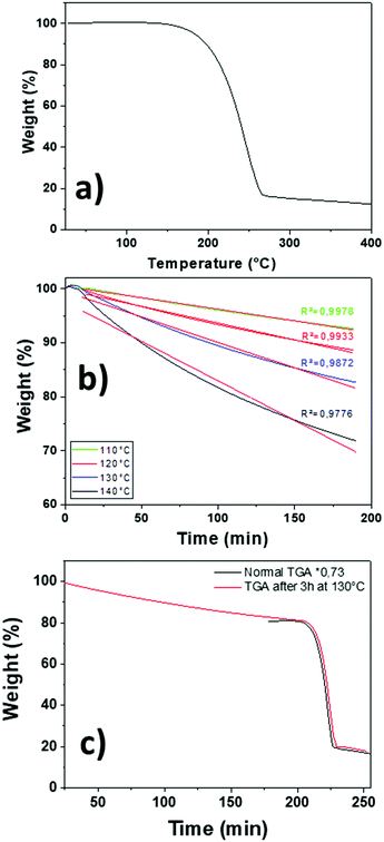
:![[thin space (1/6-em)]](https://www.rsc.org/images/entities/char_2009.gif) 0.18 has been chosen as a case study. TG dynamic analysis shows a single step indicating that the mixture evaporates in the temperature range of 140–270 °C (Fig. 1a). Compared to the bicomponent mixture used for pure BFO deposition, we noted a slight residue increase to 12% of the initial mass. Then, the mass transport property behaviour of the mixture has been investigated by isothermal gravimetric analysis. Samples were brought to set temperature, with a 5 °C min−1 heating ramp and maintained at 110 °C, 120 °C, 130 °C, and 140 °C for 3 hours (Fig. 1b). The linear fittings of the isothermal data indicate a perfectly linear behaviour for the 110 °C–120 °C temperature range, while a slight deviation has been found for the isothermal curve at 130 °C, thus confirming that the mixture performs as a “single-source” precursor. From 140 °C, the deviation starts to be visible, indicating a preferential use of the precursor mixture up to 130 °C. This has been assessed through a designed experiment: the mixture sample has been maintained for 3 hours at 130 °C and then subjected to a dynamic TG cycle. The perfect overlap of the TGA curve before ageing, normalized for the weight loss arisen after the 3 hours isothermal treatment at 130 °C, and the one obtained after ageing indicates that the mixture source is absolutely stable under harsher conditions than those applied in the MOCVD process (Fig. 1c).
0.18 has been chosen as a case study. TG dynamic analysis shows a single step indicating that the mixture evaporates in the temperature range of 140–270 °C (Fig. 1a). Compared to the bicomponent mixture used for pure BFO deposition, we noted a slight residue increase to 12% of the initial mass. Then, the mass transport property behaviour of the mixture has been investigated by isothermal gravimetric analysis. Samples were brought to set temperature, with a 5 °C min−1 heating ramp and maintained at 110 °C, 120 °C, 130 °C, and 140 °C for 3 hours (Fig. 1b). The linear fittings of the isothermal data indicate a perfectly linear behaviour for the 110 °C–120 °C temperature range, while a slight deviation has been found for the isothermal curve at 130 °C, thus confirming that the mixture performs as a “single-source” precursor. From 140 °C, the deviation starts to be visible, indicating a preferential use of the precursor mixture up to 130 °C. This has been assessed through a designed experiment: the mixture sample has been maintained for 3 hours at 130 °C and then subjected to a dynamic TG cycle. The perfect overlap of the TGA curve before ageing, normalized for the weight loss arisen after the 3 hours isothermal treatment at 130 °C, and the one obtained after ageing indicates that the mixture source is absolutely stable under harsher conditions than those applied in the MOCVD process (Fig. 1c).
FE-SEM investigation
The thin films of BFO and Dy-doped BFO have been deposited on STO:Nb substrates and present a clear aspect. BDFO film morphologies obtained through FE-SEM using secondary electron detection are reported in Fig. 2. For a lower Dy-doping content of 6%, well coalesced 500 nm squared grains are visible (Fig. 2a). For higher doping contents of 8% and 11% (Fig. 2b and c), a similar flat and homogenous morphology is visible all over the surface for both films. At higher doping, no grain boundaries are visible, suggesting an improvement of the film morphology correlated with the increase of the Dy concentration. Film thicknesses have been assessed through FE-SEM cross-sectional images. Even at higher Dy percentages, cross sections show that the grown films are not only uniform, but also very dense. BDFO samples show an average thickness of 500 nm (Fig. 2d), thus implying a growth rate of about 8 nm min−1, identical to what was previously measured for pure BFO obtained under the same process conditions.35,36 The film composition has been assessed through EDX analysis (Fig. S1, ESI†). Particular attention has been devoted to Dy quantification due to the proximity between the Dy Lα and Fe Kα peaks. To properly quantify Dy, since the EDX software does not allow the use of the Dy M peak, reasonable analysis has been done by taking advantage of the ratio between the Fe Kα and Fe L peak intensities in the pure BFO film. The evaluation of the Fe Kα and Fe L line ratios in the BDFO films, compared to the BFO reference value, allowed to proper quantification of the Bi![[thin space (1/6-em)]](https://www.rsc.org/images/entities/char_2009.gif) :
:![[thin space (1/6-em)]](https://www.rsc.org/images/entities/char_2009.gif) Dy
Dy![[thin space (1/6-em)]](https://www.rsc.org/images/entities/char_2009.gif) :
:![[thin space (1/6-em)]](https://www.rsc.org/images/entities/char_2009.gif) Fe ratio by separating the contribution of the Dy L peak in the quantification of Fe.
Fe ratio by separating the contribution of the Dy L peak in the quantification of Fe.
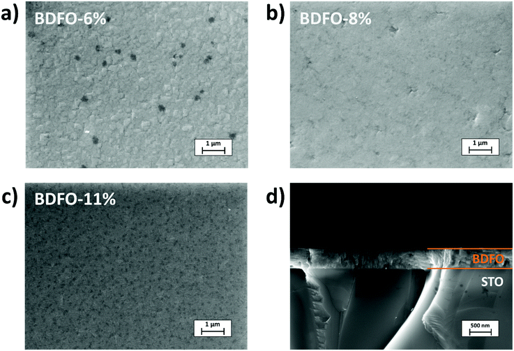 | ||
| Fig. 2 Secondary electron FE-SEM plan view images of (a) BDFO-6%, (b) BDFO-8%, (c) BDFO-11% and (d) cross-section of the BDFO-11% film. | ||
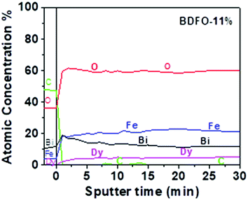
In addition, an XPS depth profile, carried out on the BDFO-11% film alternating Ar ion sputter and XPS analysis, is shown in Fig. 3. Although the absolute concentrations of the elements cannot be determined due to possible differential sputter yields, the plot indicates that the film composition is constant in the bulk of the film and no concentration gradients are present moving from the surface to the bulk.
X-Ray diffraction
An in-depth structural characterization of the BFO and BDFO deposited films has been carried out through classical Bragg–Brentano diffraction and in-plane measurements to assess the phase structure and the epitaxial nature of the films. The BFO trigonal structure with a rhombohedral cell, arh = 3.965 Å and αrh = 89.41°, can be considered as pseudocubic due to the αrh angle close to 90°.The reported reflection peaks have been indexed considering a pseudocubic notation. Large θ–2θ XRD scans acquired in the Bragg–Brentano configuration between 20° and 80° (Fig. 4) show up to the third order 00l reflections of the BFO and BDFO deposited films and those of the STO:Nb substrate.
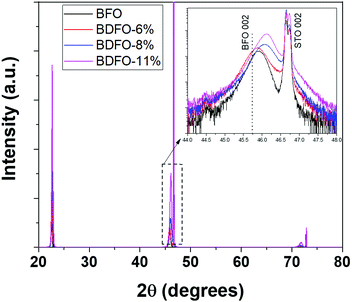 | ||
| Fig. 4 XRD θ–2θ patterns of the doped and undoped BFO films on the Nb:STO substrate. Inset: An enlarged region in the 44.0–48.0° z range. | ||
This implies the formation of a highly oriented film, deposited without any parasitic phases for the pure BFO and for all the Dy-doped BFO systems. The focus on the 002 reflection (inset in Fig. 4) shows a broadening of diffraction peaks and a shift toward higher angles as the Dy percentage increases.
Considering the remarkable out-of-plane orientation, the in-plane orientation has been investigated by recording Φ-scans of the BFO and BDFO films.
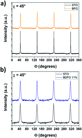
Φ-Scan patterns of the pure BFO film and the STO:Nb substrate have been recorded at χ = 45° to observe both the BFO 110 (at 2θ = 31.80°) and STO:Nb 110 (at 2θ = 32.42°) reflections (Fig. 5a). Following a similar approach, Φ-scan patterns of the Dy-doped films were recorded and as a representative example data on BDFO-11% are shown in Fig. 5b. Also, in this case, the 110 reflections of the BDFO-11% film (at 2θ = 31.84°) and of the STO:Nb substrate (at 2θ = 32.42°) have been recorded at χ = 45° (Fig. 5b). In all the cases, the correspondence of the (110) BFO or BDFO poles with the STO:Nb(110) poles demonstrates that the deposited pure BFO and BDFO films are epitaxially grown cube-on-cube on the STO(100) single crystal substrate. Numerous examples of epitaxial BFO films on STO(100) have been reported in previous studies.38,40
Following the out-of-plane study and the confirmation of the in-plane orientation of the BFO and BDFO thin films, in-plane diffraction patterns have been recorded with 2θχ/φ scans starting from 20° to 60°, so both the first order and second-order reflections of the h00 and 0k0 diffraction peaks can be observed (Fig. 6). During measurements, the ω axis has been maintained at an angle of 0.5° to limit diffraction from the STO:Nb substrate. Rotating the samples along φ (0°, 45° and 90°) allows the observation of the (h00)pc, (011)pc and (0k0)pc reflections, respectively. Diffraction patterns have been aligned on the Au 111 diffraction peak (2θχ/φ = 38.19°) (previously sputtered and acting as a reference peak), and, when visible, on STO 002 (2θχ/φ = 46.49°). The pure BFO thin film sample reveals a small component of the 011 reflection at 2θχ/φ =32.05° (Fig. 6a). All the Dy-doped systems show a good in-plane orientation. For all films, considering a cubic system, the lattice parameters have been calculated using the out-of-plane and in-plane diffraction patterns. As seen for the out-of-plane XRD pattern, Dy doping provokes a broadening of the diffraction peaks observed in-plane.
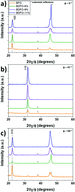 | ||
| Fig. 6 In-plane XRD patterns (ω = 0.5°) recorded for undoped BFO (orange line), BDFO-6% (green line), BDFO-8% (purple line) and BDFO-11% (blue line) films at (a) Φ = 0°, (b) Φ = 45° and Φ = 90°. | ||
As more Dy is incorporated in the film, the average A-site ionic radius is getting smaller because of the substitution of Bi3+ (r12-coord = 1.36 Å) by smaller Dy3+ (r12-coord = 1.24 Å).41,42
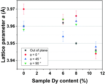
The calculated parameters for pure BFO present values very similar to the theoretical ones. Variations in the film lattice out-of-plane and in-plane parameters are directly proportional to the Dy-doping content.
Considering the pseudocubic cell, the a lattice parameter has been calculated for each deposited film thanks to the out-of-plane and in-plane diffraction patterns. Calculated values are reported and compared in Fig. 7.
For pure BFO films and up to a Dy-doping of 8%, the average value of a is relatively constant at around 3.96 Å, measured variations are caused by thermal stress. For BDFO-11%, the a lattice parameter decreases, having a value of 3.45 Å; this diminution of the lattice parameter is directly caused by reduction of the average A-site ionic radius of the BDFO film.
However, nothing indicates that the material symmetry changes toward an orthorhombic structure, as it has been reported in previous studies for the higher Dy-doping amount.16,43,44
Raman spectroscopy
The BFO hexagonal unit cell (space group R3c) is composed of 10 atoms which imply 30 (3N) vibration modes and 27 (3N − 3, 3 is the number of acoustic vibration modes) optical modes: Γopt,R3c = 4A1 + 5A2 + 9E. The modes A1 and E (two-time degenerate) are Raman and IR active and the A2 modes are silent.45–48The Raman tensors of Raman modes are given by:49
BiFeO3 is an optically uniaxial crystal, which means that the refractive index of one crystal axis (the optical axis) is different from the refractive index of the two other axis. This specific axis is called the optical axis and is parallel to the ferroelectric polarization [0001]hex || [111]pc for BiFeO3. The angle θ between the BFO optical axis and the phonon propagation vector influences directly the phonon wavenumber.48 Pure E(TO) and A1(LO) modes are visible for θ = 0° and E(LO) and A1(TO) modes for θ = 90°. In these configurations, Raman spectroscopy can detect 13 modes. In the present study, epitaxial BiFeO3 (001)pc (equivalent to (012)hex) and BDFO(001)pc films have been deposited on SrTiO3:Nb(001). Being the scattering surface different from (001)hex, it is expected to observe ordinary E(TO) phonons and phonons with a mixed symmetry LO–TO and mixed characters A1–E, dependent from the θ angle between [111]pc and the laser direction [001]pc.50–52 In this case, θ ≈ 54.7 °C and 22 modes can be observed.53,54
The Raman tensors of the Raman modes observable from the (012)hex BFO scattering surface are given by:55
In a backscattered geometry configuration for the (012)hex oriented BFO, we have the selection rules reported in Table 1.
| A1(LO + TO) | A1(TO) | E(LO + TO) | E(TO) | |
|---|---|---|---|---|
| −Z(XX)Z | X | X | ||
| −Z(XY)Z or −Z(YX)Z | X | |||
| −Z(YY)Z | X | X |
Several examples of (001)pc single crystals or thin films are reported in the literature, but in the past, the θ = 54.7° angle has been neglected and this has been the sources of controversial attribution of the vibration modes.
Based on the study of Hlinka et al.,51 Talkenbergerst et al.53 proposed a new interpretation, considering the mixed nature of the modes, of a previous work. We updated their work (Table 2) with new results obtained on the BFO single crystal along [001]pc54 and with the present study of epitaxial BFO(001)pc on STO:Nb(001).
| Phonon mode | Extraordinary phonon mode | 53 | 51 | 58 | 57 | 59 | 53 | 54 | This work −Z(XX)Z | This work Z(XY)X | |
|---|---|---|---|---|---|---|---|---|---|---|---|
| Calc.7θ = 54.7° | Single crystal (001)pc | Single crystal (001)pc | Film (001)pc | (001)pc | Film (001)pc | Single crystal (001)pc | (001)pc | (001)pc | |||
| T = 5 K | T = 4 K | T = 81 K | RT | RT | RT | RT | RT | RT | |||
| (2) | 2 | ETO (2)–A1TO (1) | 143.9 | 147 | 145 | 136 | 140 | 135 | 138 | 142.1 | 143.2 |
| (2) | 3 | A1LO (1) –ELO (2) | 176.1 | 176 | 168 | 168 | 173 | 172 | 172 | 173.7 | 175.2 |
| (2) | 4 | A1LO (2)–A1TO (2) | 224.2 | 227 | 212 | 212 | 220 | 218 | 220 | 220.2 | 222 |
| (5) | 7 | ETO (5)–A1TO (3) | 294.5 | — | 295.2 | — | 288 | — | 288 | 291.3 | 295 |
| (6) | ETO (6) | 351 | — | — | — | — | — | 347 | 348.8 | — | |
| (6) | 9 | ETO (7)–ELO (6) | 370.6 | 375 | 371.5 | 363 | 371 | 365 | 370 | 369.1 | 366.8 |
| (8) | 11 | A1LO (3)–ELO (8) | 473.7 | 473 | 473.0 | 456 | — | 465 | 470 | 469.2 | 469.8 |
| (9) | ETO (9) | 523 | 525 | 523.1 | — | 520 | 517 | 520 | 520.7 | — | |
| 12 | ETO (9)–A1TO (4) | 551.9 | — | 553 | 549 | 550 | 548 | 545 | — | 553.3 | |
| 13 | A1LO (4)–ELO (9) | 606.3 | — | — | 597 | — | — | 620 | — | 620.9 |
Typical BFO Raman spectra collected in −Z(XX)Z and −Z(XY)Z configurations are reported in Fig. 8. Between single crystals and BFO thin films, it must be noted that the epitaxial growth of BFO might induce strain on the film because of the film/substrate lattice mismatch.56 A quite relatively small mismatch of 1.53% is expected when BFO is deposited on STO. As the investigated films are 500 nm thick, such strains should be relaxed. The differences measured in mode positions are attributed to thermal stress directly linked to the deposition process. BFO and BDFO Raman spectra −Z(XX)Z are compared in Fig. 9, where, for the 3 modes E(2TO)–A1(1TO), A1(1LO)–E(2LO) and A1(2LO)–A1(2TO), a clear wavenumber shift and variations of peak widths are visible. Under the same measurement conditions, a decrease of the Raman intensity signal is observed, and it is directly caused by the change of the BDFO bandgap value with respect to BFO (from 2.68 eV to 2.25 eV, see Fig. 10).
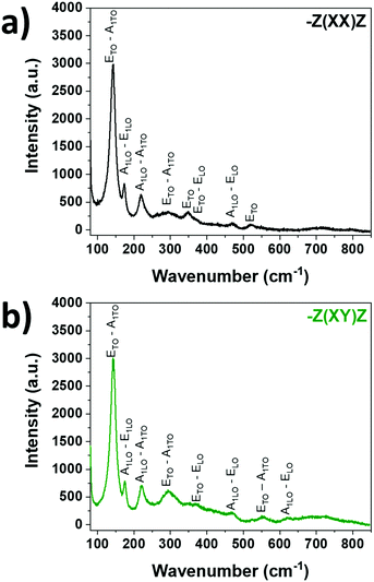 | ||
| Fig. 8 Raman spectra of the pure BFO(001)pc thin film on STO:Nb(100) collected in (a) −Z(XX)Z and (b) −Z(XY)Z configurations. | ||
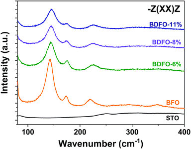 | ||
| Fig. 9 Raman spectra of BFO and BDFO(001)pc thin films on STO:Nb(001) collected in the HH configuration. | ||
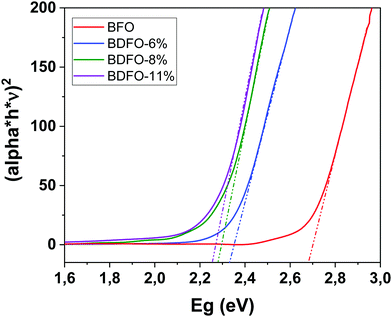 | ||
| Fig. 10 Tauc's plots of the undoped and Dy-doped BFO thin films calculated from UV-vis absorption spectra. | ||
Thus, as the Dy-doping concentration increases in the films, the excitation laser is more and more absorbed leading to a diminution of the signal. The peak attribution for the Raman spectra of the Dy-doped films has been done considering a trigonal structure similar to the one of the pure BFO. Because of the similarities between spectra recorded in −Z(XX)Z or −Z(XY)Z, mode positions in Table 3 are from the (HH) spectra.
| Phonon mode | Extraordinary phonon mode | BFO | BDFO-6% | BDFO-8% | BDFO-11% | |
|---|---|---|---|---|---|---|
| (001)pc | (001)pc | (001)pc | (001)pc | |||
| RT | RT | RT | ||||
| (2) | 2 | ETO (2)–A1TO (1) | 142.1 | 144 | 144.5 | 142.1 |
| (2) | 3 | A1LO (1)–ELO (2) | 173.7 | 175.28 | 174.8 | 174.8 |
| (2) | 4 | A1LO (2)–A1TO (2) | 220.2 | 224.1 | 224.1 | 224.6 |
| (3) | ETO (3) | — | 235.1 | 234.4 | 233.3 | |
| (5) | 7 | ETO (5)–A1TO (3) | 288 | 297.2 | 296.7 | 304.3 |
| (6) | ETO (6) | 348.8 | 349.7 | 355.3 | 346.4 | |
| (6) | 9 | ETO (7)–ELO (6) | 369.1 | 361.4 | 361.93 | 356.4 |
| (7) | 10 | ETO (8)–ELO (7) | — | 425.7 | 432.3 | 435.3 |
| (8) | 11 | A1LO (3)–ELO (8) | 469.2 | 473.9 | 476.8 | 478.4 |
| (9) | ETO (9) | 520.7 | 526.3 | 520.7 | 521.8 | |
| (9) | 13 | A1LO (4)–ELO (9) | — | 618.5 | 619.6 | 616.9 |
Present XRD analysis suggested that, despite a slight distortion of the lattice parameter, the deposited films do not present a phase transition toward an orthorhombic system as it has been reported in previous work.16 Moreover, a comparison of the present data to the previously reported Raman spectra of orthorhombic BDFO powder clearly indicates that the film deposited in this work present a trigonal structure.44 Raman spectra further confirm the previous conclusion that Dy-doping does not provoke a symmetry change but only a lattice distortion, confirming the influence of Dy on film structures.
Bandgap
The optical absorption of the MOCVD deposited BFO and BDFO films has been measured using a UV-vis spectrometer, and then the optical bandgap value has been obtained using Tauc's equation.60,61 Films have been deposited on a transparent substrate of SrTiO3(100). As the Dy percentage increases, the dopant impact on the bandgap value seems to be reduced and tends to a limit (Table 4).| BiFeO3 | 2.68 eV |
| BDFO-6% | 2.33 eV |
| BDFO-8% | 2.28 eV |
| BDFO-11% | 2.25 eV |
The film bandgap has been extrapolated from the plot of (α*h*ν)1/nvs. (h*ν), with n = 1/2 (because of the BFO direct bandgap), α, h and ν being the film absorption coefficient, Planck's constant and the photon frequency, respectively.61 For (α*h*ν)2 = 0, the linear region fitted curve show a film bandgap of 2.68 eV, which indicates a maximum absorption for a wavelength of 460 nm (Fig. 10). The reported optical bandgap values for the pure trigonal BFO film range from 2.01 eV to 2.82 eV, the variation being related to deposition methods and used substrates.62,63 The same approach has then been applied to Dy-doped BFO thin films, also deposited on transparent STO. Tauc's plots of all the studied samples are shown in Fig. 10, where the influence of Dy doping on the material bandgap can be observed. First, Dy-doping of 6% has a strong impact on the material bandgap, inducing an important reduction of its value up to 2.33 eV. Dy-Doping contents of 8% and 11% also have a noticeable influence on the bandgap, bringing it to 2.28 eV and 2.25 eV, respectively.
Piezoresponse force microscopy
The piezoelectric and ferroelectric properties of the BDFO films have been investigated through piezoresponse force spectroscopy (PFS) and piezoresponse force microscopy (PFM). Previous studies have already reported PFM and PFS investigations of MOCVD-grown BFO thin films on STO:Nb 001 and have described good and stable piezoelectric and ferroelectric properties with a 2 V coercive voltage.38 The attention has been focused on the new BDFO systems (6%, 8%, and 11%) to explore the Dy-doping effect on piezoelectric and ferroelectric properties.Single-point PFS has been measured by applying a ± 9 V round trip on the sample between the cantilever tip and the sample conductive substrate (Fig. 11). The measured piezoresponse amplitude (Mag) is a function of the applied oscillating voltage (Vac) for a defined bias voltage, from −9 V to 9 V.
 | ||
| Fig. 11 PFS of the BDFO thin films: (a) BDFO-6%, (b) BDFO-8% and (c) BDFO-11%. The piezoelectric response (Mag) of films is reported as black curves and phase switching of films as red curves. | ||
Fig. 11 shows typical butterfly loops, a characteristic of the film piezoelectric behaviour, obtained for BDFO-6% and BDFO-8%. Local ferroelectric switching (Phase) is reported for the same samples and corresponds to the phase difference between Vac and the induced vertical piezoresponse signal from the sample at a different bias voltage. The piezoelectric and phase responses measured for BDFO-6% are similar to what was previously measured for the pure BFO films.8 Compared to the other samples, BDFO-8% shows that the internal polarization of the film benefits of a significant increase as the opening of the phase and Mag loops is much wider. The reproducibility of the process is confirmed by the identical piezoelectric properties observed for two different BDFO-6% (Fig. S2, ESI†) and two different BDFO-8% (Fig. S3, ESI†) samples.
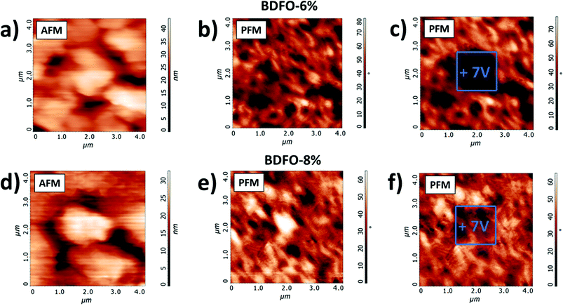
Local measurements showed promising piezoelectric and ferroelectric properties for BDFO-6% and BDFO-8%. To go further in this investigation, we decided to perform a writing experiment to map samples of the ferroelectric domain. On the other hand, BDFO-11% did not show a significative response, so no writing experiment was attempted.
Atomic force microscopy (AFM) topography scans of the studied 4 μm × 4 μm BDFO-6% and BDFO-8% samples are shown in Fig. 12a and d, respectively. Simultaneously, phase maps of the ferroelectric domains of the “as-deposited” films were recorded by using Vac = 0.9 V at a 0 V bias voltage (Fig. 12b and e). A 7 V bias was then applied to the films from the PFM tip on a smaller 1 μm × 1 μm area. After writing, the new phase image of the larger 4 μm × 4 μm area has been recorded at 0 V bias voltage to observe the switching of ferroelectric domains. The areas exposed to the 7 V bias show a significant phase switching (Fig. 12c and f) compared to the initial phase scan, thus confirming the ferroelectric nature of the BDFO-6% and BDFO-8% samples.
PFM and PFS investigations have demonstrated that the Dy-doping can have a noticeable impact on the functional properties of the BDFO films, but, above 8% Dy doping, a diminution of the film ferroelectric and piezoelectric behaviours is evident.
These findings are in good accordance with the other data reported in this work. All films are epitaxially grown and are highly homogeneous, but, for BDFO-11%, even if no change in the material symmetry is measured, the influence of the smaller Dy3+ ion with respect to Bi3+ on the structure was measured and induced a diminution of the a parameter of the pseudocubic cell.
Film bandgap values also confirm this trend with a tunability which finds its limit for a Dy percentage of 11%, but with a value merely lower than the one measured for BDFO-8%.
Conclusions
This work aims to present the tuning of the MOCVD route for the deposition of undoped and Dy-doped BiFeO3 on the SrTiO3:Nb(100) substrate. The impact of dysprosium doping on the film structure, bandgap, and ferroelectric and piezoelectric properties has been described for pure BFO films and three different Dy-doping levels: Bi1−xDyxFeO3 (x = 0, 0.06, 0.08 and 0.11). The good thermal properties and volatility of the tri-metallic precursor mixture have been established, enabling the deposition of epitaxial dense 500 nm thick films.Dy-Doping has a clear impact on thin film structures, confirmed by in-plane and out-of-plane XRD and Raman spectroscopy, but, even at x = 0.11, no phase transition is visible in the material. For the pure BFO film, the optical bandgap is 2.68 eV, but a reduction up to 2.25 eV was observed for the 11% Dy percentage. The ferroelectric and piezoelectric responses show an improvement of up to x = 0.08; above this dopant amount, for x = 0.11, films seem to lose their ferroelectric response and so their piezoelectric properties.
Conflicts of interest
There are no conflicts to declare.Acknowledgements
This work was supported by the European Community under the Horizon 2020 Programme in the form of the MSCA-ITN-2016 ENHANCE Project, Grant Agreement No. 722496. The authors thank the Bio-nanotech Research and Innovation Tower (BRIT) laboratory of the University of Catania (Grant no. PONa3_00136 financed by the MIUR) for the Smartlab diffractometer and PHI 5000 Versa probe XPS facility.References
- G. Catalan and J. F. Scott, Adv. Mater., 2009, 21, 2463–2485 CrossRef CAS.
- T. Choi, S. Lee, Y. J. Choi, V. Kiryukhin and S. W. Cheong, Science, 2009, 324, 63–66 CrossRef CAS PubMed.
- A. Queraltó, R. Frohnhoven, S. Mathur and A. Gómez, Appl. Surf. Sci., 2020, 509, 144760 CrossRef.
- Y. Ji, T. Gao and L. W. Zhong, Nano Energy, 2019, 64, 103909 CrossRef CAS.
- G. T. Hwang, V. Annapureddy, J. H. Han, D. J. Joe, C. Baek, D. Y. Park, D. H. Kim, J. H. Park, C. K. Jeong, K. I. Park, J. J. Choi, D. K. Kim, J. Ryu and J. Lee, Adv. Energy Mater., 2016, 6, 1600237 CrossRef.
- P. Muralt, R. G. Polcawich and S. Trolier-McKinstry, MRS Bull., 2009, 34, 658–664 CrossRef CAS.
- Q. Wang, C. R. Bowen, W. Lei, H. Zhang, B. Xie, S. Qiu, M. Y. Li and S. Jiang, J. Mater. Chem. A, 2018, 6, 5040–5051 RSC.
- M. R. Catalano, G. Spedalotto, G. G. Condorelli and G. Malandrino, Adv. Mater. Interfaces, 2017, 4, 1601025 CrossRef.
- S. Wu, J. Zhang, X. Liu, S. Lv, R. Gao, W. Cai, F. Wang and C. Fu, Nanomaterials, 2019, 9, 190 CrossRef CAS PubMed.
- D. Kan, L. P. lova, V. Anbusathaiah, C. J. Cheng, S. Fujino, V. Nagarajan, K. M. Rabe and I. Takeuchi, Adv. Funct. Mater., 2010, 20, 1108–1115 CrossRef CAS.
- A. Radojković, D. L. Golić, J. Ćirković, Z. M. Stanojević, D. Pajić, F. Torić, A. Dapčević, P. Vulić, Z. Branković and G. Branković, Ceram. Int., 2018, 44, 14 CrossRef.
- C. S. Tu, P. Y. Chen, C. S. Chen, C. Y. Lina and V. H. Schmidt, J. Eur. Ceram. Soc., 2018, 38(4), 1389–1398 CrossRef CAS.
- X. Yuan, L. Shi, J. Zhao, S. Zhou, J. Guo, S. Pan, X. Miao and L. Wu, Phys. Status Solidi B, 2018, 1800499 Search PubMed.
- Y. Zhang, H. Zheng, X. Wang, H. Li, Y. Wu, Y. Zhang, H. Su and G. Yuan, Ceram. Int., 2020, 46, 8A CrossRef.
- Q. Wang, C. R. Bowen, W. Lei, H. Zhang, B. Xie, S. Qiu, M. Y. Li and S. Jiang, J. Mater. Chem. A, 2018, 6, 5040–5051 RSC.
- A. Kumar, P. Sharma and D. Varshney, J. Ceram., 2015, 8, 869071 Search PubMed.
- Q. Micard, G. Clementi, A. Bartasyte, P. Muralt, G. G. Condorelli and G. Malandrino, Adv. Mater. Interfaces, 2022, 2101539, DOI:10.1002/admi.202101539.
- Y. Li, J. Yu, J. Li, C. Zheng, Y. Wu, Y. Zhao, M. Wang and Y. Wang, J. Mater. Sci.: Mater. Electron., 2011, 22, 323–327 CrossRef CAS.
- S. S. Chowdhury, A. H. M. Kamal, R. Hossain, M. Hasan, Md. F. Islam, B. Ahmmad and M. A. Basith, Ceram. Int., 2017, 43, 9191–9199 CrossRef CAS.
- Q. Micard, A. L. Pellegrino, R. Lo Nigro, A. Bartasyte, G. G. Condorelli and G. Malandrino, J. Mater. Chem. C, 2020, 8, 16168–16179 RSC.
- Q. Zhang, W. Cai, Q. Li, R. Gao, G. Chen, X. Deng, Z. Wang, X. Cao and C. Fu, J. Alloys Compd., 2019, 794, 542–552 CrossRef CAS.
- T. Fan, C. Ji, G. Chen, W. Cai, R. Gao, X. Deng, Z. Wang and C. Fu, Mater. Chem. Phys., 2020, 250, 123034 CrossRef CAS.
- H. Uchida, N. Kaneko, S. Yasui and H. Funakubo, Jpn. J. Appl. Phys., 2018, 57, 0902B5 CrossRef.
- A. Singh, Z. R. Khan, P. M. Vilarinho, V. Gupta and R. S. Katiyare, Mater. Res. Bull., 2014, 49, 531–536 CrossRef CAS.
- S. Sharma, A. Sharma, V. Gupta, N. K. Puri and M. Tomar, J. Electron. Mater., 2021, 50, 1835–1844 CrossRef CAS.
- H. Wang, J. Huang, X. Sun, J. Jian, J. Liu and H. Wang, RSC Adv., 2020, 10, 40229–40233 RSC.
- E. B. Agustina, Y. Iriani and R. Suryana, J. Phys.: Conf. Ser., 2019, 1397, 012002 CrossRef CAS.
- A. Abramov, D. Alikin, A. Sobol, D. Myakishev, V. Slabov, L. Trusov, V. Safina, A. Turygin, A. Vasiliev, V. Shur and A. Kholkin, Coatings, 2020, 10(5), 438 CrossRef CAS.
- Z. Hanfei, M. Hongfang and Z. Yuyao, Vacuum, 2018, 157, 428–432 CrossRef.
- T. C. Kim, S. H. Lee, H. K. Jung, Y. E. Kim, J. W. Choi, D. Yang and D. H. Kim, J. Magn. Magn. Mater., 2019, 471, 116–123 CrossRef CAS.
- K. S. Kumar, A. Sudharani, M. Ramanadha, S. Ramu, G. Murali and R. P. Vijayalakshmi, Mater. Sci. Eng., B, 2021, 270, 115235 CrossRef.
- X. Deng, Z. Zeng, R. Gao, Z. Wang, G. Chen, W. Cai and C. Fu, J. Alloys Compd., 2020, 831, 154857 CrossRef CAS.
- M. S. Kartavtseva, Y. Gorbenko, A. R. Kaul and T. V. Murzina, Thin Solid Films, 2010, 518, 4750–4752 CrossRef CAS.
- N. Deepak, P. Carolan, L. Keeney, P. F. Zhang, M. E. Pemble and R. W. Whatmore, Chem. Mater., 2015, 27, 6508–6515 CrossRef CAS.
- D. Scillato, N. Licciardello, M. R. Catalano, G. G. Condorelli, R. Lo Nigro and G. Malandrino, J. Nanosci. Nanotechnol., 2011, 11, 8221–8225 CrossRef CAS PubMed.
- J. A. S. Moniz, R. Quesada-Cabrera, C. S. Blackman, J. Tang, P. Southern, P. M. Weaver and J. C. Carmalt, J. Mater. Chem. A, 2014, 2, 2922–2927 RSC.
- G. Malandrino and I. L. Fragala, Coord. Chem. Rev., 2006, 250, 1605–1620 CrossRef CAS.
- G. G. Condorelli, M. R. Catalano, E. Smecca, R. Lo Nigro and G. Malandrino, Surf. Coat. Technol., 2013, 230, 168–173 CrossRef CAS.
- Q. Micard, G. G. Condorelli and G. Malandrino, Nanomaterials, 2020, 10, 630 CrossRef CAS PubMed.
- J. Wang, J. B. Neaton, H. Zheng, V. Nagarajan, S. B. Ogale, B. Liu, D. Viehland, V. Vaithyanathan, D. G. Schlom, U. V. Waghmare, N. A. Spaldin, K. M. Rabe, M. Wuttig and R. Ramesh, Science, 2003, 299, 1719–1722 CrossRef CAS PubMed.
- Y. Q. Jia, J. Solid State Chem., 1991, 95, 184–187 CrossRef CAS.
- T. Durga Rao, T. Karthik and S. Asthana, J. Rare Earths, 2013, 31, 370–375 CrossRef.
- V. A. Khomchenko, D. V. Karpinsky, A. L. Kholkin, N. A. Sobolev, G. N. Kakazei, J. P. Araujo, I. O. Troyanchuk, B. F. O. Costa and J. A. Paixão, J. Appl. Phys., 2010, 108, 074109 CrossRef.
- M. Muneeswaran and N. V. Giridharan, J. Appl. Phys., 2014, 115, 214109 CrossRef.
- D. Rout, K. S. Moon and S. J. L. Kang, J. Raman Spectrosc., 2009, 40, 618–626 CrossRef CAS.
- M. K. Singh, S. Ryu and H. M. Jang, Phys. Rev. B: Condens. Matter Mater. Phys., 2005, 72, 132101 CrossRef.
- M. N. Iliev, M. V. Abrashev, D. Mazumdar, V. Shelke and A. Gupta, Phys. Rev. B: Condens. Matter Mater. Phys., 2010, 82, 014107 CrossRef.
- G. L. Yuan, S. W. Or and H. L. W. Chan, J. Phys. D: Appl. Phys., 2007, 40, 1196 CrossRef CAS.
- R. Claus, L. Merten and J. Brandmüller, Light Scattering by Phonon-Polaritons, Springer, Berlin, 1975 Search PubMed.
- E. Borissenko, M. Goffinet, A. Bosak, P. Rovillain, M. Cazayous, D. Colson, P. Ghosez and M. Krisch, J. Phys.: Condens. Matter, 2013, 25, 102201 CrossRef PubMed.
- J. Hlinka, J. Pokorny, S. Karimi and I. M. Reaney, Phys. Rev. B: Condens. Matter Mater. Phys., 2011, 23, 020101 CrossRef.
- H. Fukumura, S. Matsui, H. Harima, T. Takahashi, T. Itoh, K. Kisoda, M. Tamada, Y. Noguchi and M. Miyayama, J. Phys.: Condens. Matter, 2007, 19, 365224 CrossRef CAS PubMed.
- A. Talkenberger, I. Vrejoiu, F. Johann, C. Röder, G. Irmer, D. Rafaja, G. Schreiber, J. Kortus and C. Himcinschi, J. Raman Spectrosc., 2015, 46, 1245–1254 CrossRef CAS.
- C. Himcinschi, J. Rix, C. Röder, M. Rudolph, M. Yang, D. Rafaja, J. Kortus and M. Alexe, Sci. Rep., 2019, 9, 379 CrossRef PubMed.
- M. I. Aroyo, J. M. Perez-Mato, D. Orobengoa, E. Tasci, G. de la Flor and A. Kirov, Bulg. Chem. Commun., 2011, 43(2), 183–197 CAS.
- K. Streiffer, C. B. Parker, A. E. Romanov, M. J. Lefevre, L. Zhao, J. S. Speck, W. Pompe, C. M. Foster and G. R. Bai, J. Appl. Phys., 1998, 83, 5 CrossRef.
- M. K. Singh, Hyun M. Jang, S. Ryu and M. Jo, Appl. Phys. Lett., 2006, 88, 042907 CrossRef.
- R. Palai, H. Schmid, J. F. Scott and R. S. Katiyar, Phys. Rev. B: Condens. Matter Mater. Phys., 2010, 81, 139903 CrossRef.
- C. Beekman, A. A. Reijnders, Y. S. Oh, S. W. Cheong and K. S. Burch, Phys. Rev. B: Condens. Matter Mater. Phys., 2012, 86, 020403 CrossRef.
- J. Tauc, R. Grigorovic and A. Vancu, Phys. Status Solidi, 1966, 15, 627 CrossRef CAS.
- B. D. Viezbicke, S. Patel, B. E. Davis and D. P. Birnie, Phys. Status Solidi B, 2015, 252, 1700–1710 CrossRef CAS.
- D. Sando, C. Carrétéro, M. N. Grisolia, A. Barthélémy, V. Nagarajan and M. Bibes, Adv. Opt. Mater., 2017, 1700836 Search PubMed.
- J. Chakrabartty, R. Nechache, C. Harnagea, S. Li and F. Rosei, Nanotechnology, 2016, 27, 215402 CrossRef PubMed.
Footnotes |
| † Electronic supplementary information (ESI) available: EDX spectra and PFM measurements. See DOI: 10.1039/d1ma01088c |
| ‡ Current address: FEMTO-ST Institute, University of Bourgogne Franche-Comté CNRS UMR 6174, 26 Rue de l’Epitaphe, F-25030 Besançon, France. |
| This journal is © The Royal Society of Chemistry 2022 |

