
Structure and electronic properties of C2N/graphene predicted by first-principles calculations
Dandan Wanga,
DongXue Han*a,
Lei Liu b and
Li Niua
b and
Li Niua
aState Key Laboratory of Electroanalytical Chemistry, c/o Engineering Laboratory for Modern Analytical Techniques, Changchun Institute of Applied Chemistry, Chinese Academy of Science, Changchun, 130022, Jilin, China. E-mail: dxhan@ciac.ac.cn; Fax: +86 431852628 00; Tel: +86 4318526 2425
bState Key Laboratory of Luminescence and Applications, CIOMP, Chinese Academy of Sciences, No. 3888 Dongnanhu Road, Changchun, 130033, Jilin, China
First published on 14th March 2016
Abstract
The zero band gap of pristine graphene hinders its application in high-performance field effect transistors (FETs) at room temperature. The symmetry breaking of the sub-lattice, originated from the influence of substrates such as silicon carbide, hexagonal boron nitride as well as graphitic carbon nitride (C3N4), can produce a band gap in graphene. Herein, another novel kind of substrate, C2N, is employed to break the symmetry of the graphene sub-lattice, resulting in a band gap of about 0.40 eV in graphene. In combination with C2N through the weak van der Waals (vdW) interaction, graphene keeps its structural integrity and charge mobility. A band opening as large as 0.72 eV could be achieved through reducing the layer spacing to 3.2 Å. This is because the amount of electron transfer from graphene to C2N and the interaction between C2N and graphene increase with the decreasing interlayer spacing. Moreover, though the band gap of C2N is slightly altered, its electronic properties especially the direct band gap in visible region and the band dispersions are almost preserved. Thus, our theoretical results predict the promising multifunctional applications of C2N/graphene (C2N/G) heterostructures, including high-performance FETs and metal-free photocatalytic materials for water splitting.
1. Introduction
Graphene has attracted a lot of attention due to its structural features and excellent electron transport properties.1–3 What's more, high quality large-area graphene sheets can be obtained through a number of techniques, for example, mechanical exfoliation of pyrolytic graphite,1,3 chemical reduction of graphene oxides,4,5 confinement controlled sublimation of silicon carbide,6,7 chemical vapor deposition (CVD) on metal substrate8 etc. Thus graphene has been considered as a strong contender for a channel material, replacing silicon, in the next generation of high-speed and low power consumption optoelectronic devices.9–12 However it's utilization in electronic devices especially in high speed FETs is limited because logic devices with channels made of large-area graphene cannot be switched off due to the zero band gap.3,13It has been demonstrated that the lack of band gap originates from the sub-lattice symmetry in graphene.14 To open the band gap of graphene, many techniques have been utilized to break the symmetry, such as defect generation,15,16 chemical doping17,18 and graphene ceramics19 etc. However, the structural integrity of graphene is usually damaged by those approaches and as a result the charge transport in graphene is negatively influenced.20,21 Fortunately, an alternative route to induce the sub-lattice symmetry breaking while preserve the structural integrity and the electronic properties in graphene is placing graphene on an appropriate substrate. For example, Zhou et al. have demonstrated that a band gap of about 0.26 eV is created for the graphene which was epitaxially grown on SiC substrate22 owing to the graphene–substrate interaction. Moreover, the atomically flat two-dimensional materials which are free from dangling bonds are alternative substrates for graphene. Previous first-principles calculations suggested that a band gap of 0.1 eV can be opened up when graphene is Bernal stacked on hexagonal boron nitride (hBN) substrate.23 Experimentally, the mobility of charge carriers in hBN supported graphene is improved compared to that of SiO2 supported graphene.24 Though the band gap is opened without degrading the electronic properties in graphene through those approaches, the obtained band opening is usually smaller than 0.34 eV,25 not big enough for the application in the channel material in a FET.13 Therefore new strategies are required to develop for bigger band opening in graphene.
Recently, J. Mahmood et al. successfully synthesized a layered two-dimensional network structure of C2N-h2D and the single-layer C2N-h2D crystal was also obtained by them on a Cu(111) substrate under ultrahigh vacuum conditions.26 Subsequently, C2N-h2D has been demonstrated to be potential candidates for porous membrane for hydrogen purification,27 visible light responding photocatalyst for water splitting,28 nanoscale electronic and other optoelectronic devices.29 Considering the flat two-dimensional structure of C2N-h2D,26 it's expected intuitively that the C2N-h2D can be used as a substrate for graphene and the sub-lattice symmetry in graphene will break due to the evenly distributed holes and nitrogen atoms in C2N-h2D. We should also note that the epitaxial growth of graphene on Cu(111) surfaces via chemical vapor deposition is known to be one of the most reliable routes toward high-quality large-area graphene.30,31 Therefore the obtain of C2N/G heterostructures is possible via chemical vapor deposition technique.
In this work, we design C2N/G heterostructures and perform first-principles calculations to investigate their structure and electronic properties. To obtain the accurate electronic structures, hybrid functional calculations using HSE06 functional have been employed. Our calculations demonstrate, for the first time, that a gap of about 0.40 eV is opened in C2N supported graphene and there is a significant electron transfer from graphene layer to C2N layer. The interlayer interaction can induce tunable band gap in graphene by altering the interlayer spacing. We also find that the electric properties of C2N, especially the direct band gap in visible region, are almost preserved. These results suggest that the C2N/G heterostructures can be used both as an electric material for high-performance FETs and as a visible light responding photocatalyst in water splitting.
2. Computational method
Our theoretical calculations are based on density functional theory (DFT) within the Perdew–Burke–Ernzerhof (PBE) generalized gradient approximation32 and the projected augmented wave (PAW) method as implemented in the Vienna ab initio simulation package (VASP).33,34 In all calculations, the cutoff energy for the plane wave basis set is 400 eV, and a vacuum region of 15 Å is used in building the slab models to avoid the interaction between two adjacent periodic images. For the structure optimization, the special K-point sampling with a K-point separation of <0.04 Å−1 is applied for the Brillouin-zone integration, and atomic positions are relaxed until their residual forces are less than 0.01 eV Å−1. To describe the long-range van der Waals (vdW) interactions, the second version of vdW-DF (vdWDF2) of Langreth and Lundqvist groups35–38 is used. What's more, we have employed hybrid functional calculations using HSE06 functional39 to obtain the accurate electronic structures.3. Results and discussion
3.1. Structure properties of C2N/G
We simulate the C2N/G heterostructures by combining (2√3 × 2√3) unit cells of graphene and (1 × 1) unit cell of C2N in a supercell. Two stacking sequences are considered, as shown in Fig. 1. Fig. 1(a) exhibits AA stacking arrangement with all C and N atoms of C2N layer right above C atoms of graphene layer. Fig. 1(b) has AB stacking sequence with half of the C or N atoms of the C2N right above C atoms of graphene, while another half of the atoms are on the top of the centers of graphene hexagons. Binding energies are estimated to determine the interlayer interaction using the equation Eb = EHS − EG − EC2N, where Eb is the binding energy, EHS is the total energy of the heterostructure, and EG and EC2N are the total energies of the isolated graphene and C2N constituent layer respectively. The equilibrium interlayer spacing of AA and AB stacking heterostructures is 3.60 Å and 3.57 Å with small binding energies of −42.7 meV and −45.3 meV per atom of graphene respectively. To validate these results, the interlayer distance of bilayer graphene is calculated to be 3.61 Å with the same method and this result agrees well with reported theoretical studies.40 The small binding energies suggest that C2N and graphene combine through a weak vdW interaction without any new chemical bonds at the interfaces.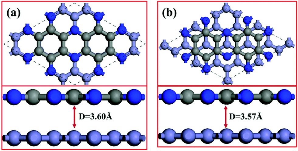 | ||
| Fig. 1 Top (top panels) and side (bottom panels) views of lattice structures of the C2N/G heterostructures: (a) AA stacking sequence, (b) AB stacking sequence. The C atoms of graphene layer are represented by the light gray balls and those of C2N layer are denoted as dark gray balls. The N atoms are indicated by blue balls. | ||
3.2. Electronic properties of C2N/G
Besides the electronic properties C2N/G heterostructures, we first calculate the electronic structures of graphene (2√3 × 2√3) supercell and C2N unit cell. For graphene (2√3 × 2√3) supercell, the gapless characteristic is retained while the Dirac points move to the Γ point from the K point, as shown in Fig. 2(a). This Dirac point movement agrees with the 3N rule for the electronic properties of graphene, which has been verified.41 Our calculations demonstrate that pristine C2N monolayer is a direct semiconductor and the calculated band gap is 2.49 eV, seen from Fig. 2(b), which is consistent with the previous experimental and theoretical results.26,29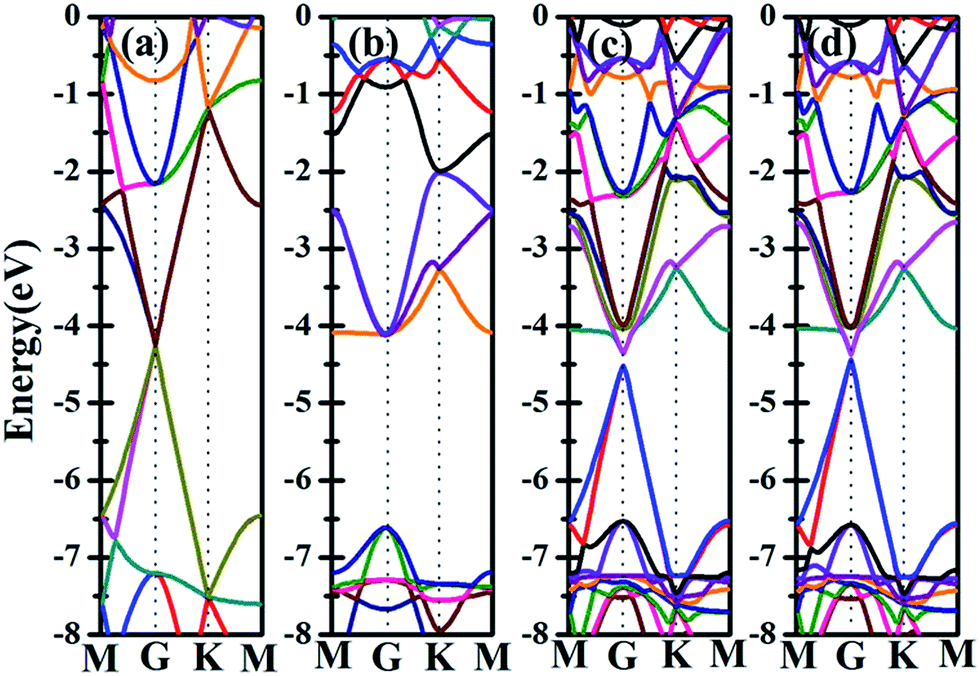 | ||
| Fig. 2 Band structures for (a) monolayer graphene (2√3 × 2√3) supercell, (b) monolayer C2N unit cell, (c) C2N/G heterostructure with AA stacking sequence and (d) C2N/G heterostructure with AB stacking sequence. The vacuum level is set at 0 eV. | ||
Sequentially, we study the electronic properties of C2N/G heterostructures. The corresponding band structures for the two stacking configurations shown in Fig. 1 are presented in Fig. 2(c) and (d). Similar behaviors have been found for the two stacking structures and the band gap of the heterostructures is quite small (about 0.1 eV). Comparing the band structures of C2N/G heterostructures with those of isolated monolayers, as shown in Fig. 2, we find the CBM and VBM of the C2N/G are localized in C2N and graphene respectively. Further analysis of total density of states (TDOS) and localized density of states (LDOS) as shown in Fig. 3 indicates the VBM originates from the pz states of C atoms. Through the band-decomposed charge density calculations which are not shown here, we find these C atoms belong to the graphene component. Furthermore the CBM is constituted by the hybrid pz states of C and N atoms which are from the C2N constituent layer.
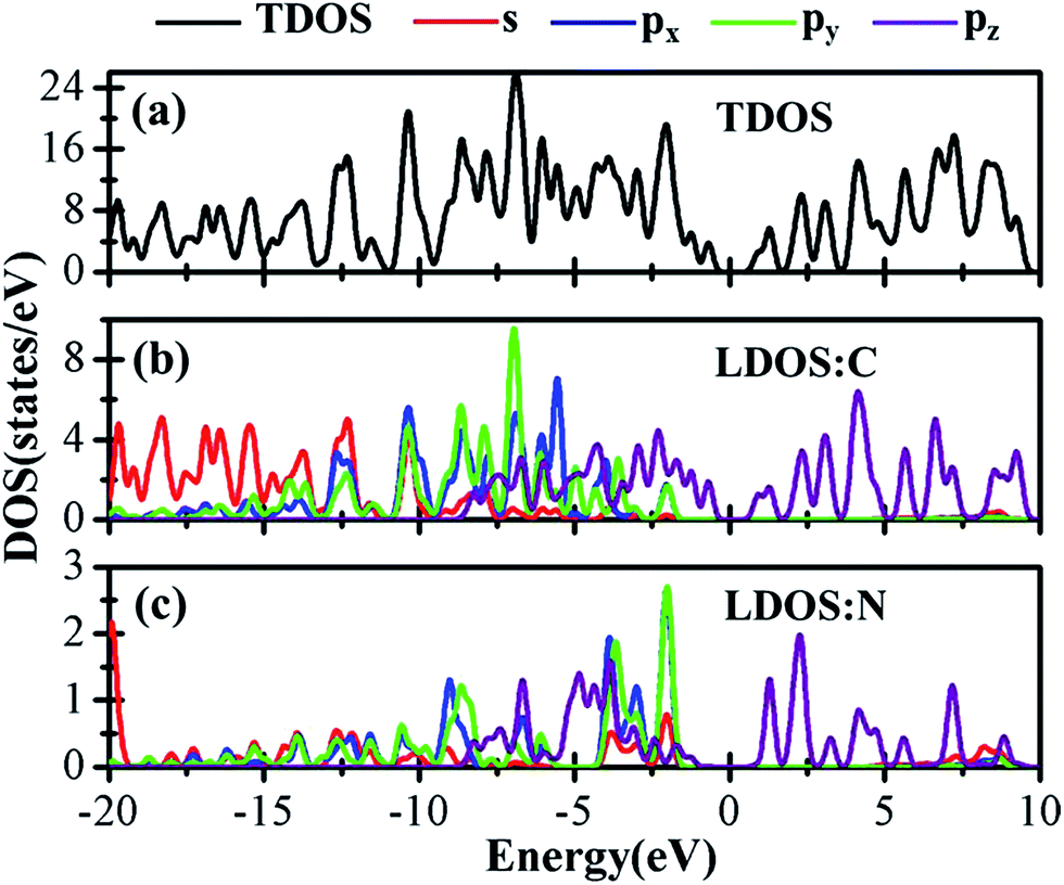 | ||
| Fig. 3 TDOS and LDOS of the C2N/G heterostructures. (a) TDOS, (b) the electronic states of C atoms, (c) the electronic states of N atoms. The red, blue, green and purple lines are representative for s, px, py, pz states respectively. The electronic properties of AA and AB stacking sequence are similar, except for the small gap between the VBM of graphene and the CBM of C2N. Therefore only the DOS of C2N/G in AB stacking is shown here. | ||
Further examination on the band characterizations indicates that the band dispersion of C2N in heterostructures is preserved while its band gap reduces to 2.20 eV. And a band gap of 0.47 eV and 0.41 eV at the Γ point emerges for the C2N supported graphene in AA and AB stacking sequence, respectively. In order to understand the mechanism of the band gap opening for graphene, the interfacial electronic properties between the C2N and graphene layers are analyzed. Fig. 4(a) presents the plane-averaged electrostatic potential along the perpendicular direction of the C2N/G heterostructures. We find the potential drop (ΔV) across the C2N/G interface is 6.57 V, which indicates a strong electrostatic field and electron/hole accumulation at the two different constituent layers. From the three-dimensional charge density difference plots shown in Fig. 4(b) and (c), which are constructed by subtracting the C2N/G electronic charge from those of the isolated components, we can clearly see that the graphene layer denotes electrons to the C2N layer. The amount of electron transfer is calculated to be 0.13 e (about 0.005 e per C atom of graphene). This electron transfer results in p-doping in graphene while n-doping in C2N. It is noteworthy that circular-shaped hole-rich regions periodically distribute in the graphene layer due to the periodic holes and nitrogen atoms in planar C2N. This charge periodicity implying the sub-lattice symmetry break disrupts the degeneracy of the π and π* bands of graphene at the Γ point, which plays an important role in the band gap opening. What's more, the band curvature around the Dirac point of the C2N supported graphene is very similar to that of pristine graphene (see Fig. 2(a), (c) and (d)), which indicates that the effective mass of electron/hole and the charge mobility are not significantly influenced by the C2N support.
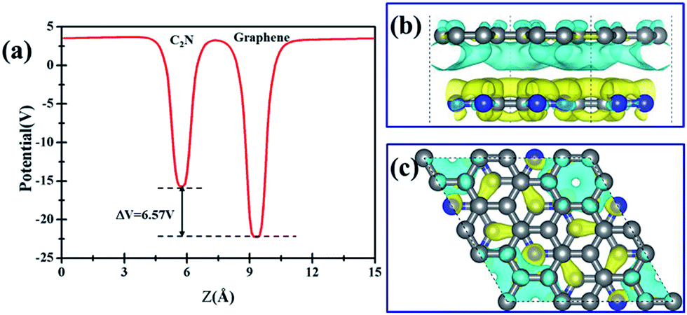 | ||
| Fig. 4 Charge transfer properties: (a) potential profile across the interface for the C2N/G heterostructures. (b) Front view and (c) top view of the isosurface of the difference charge density with the isovalue of 0.003 Å−3. The blue (yellow) color denotes loss (gain) of electrons. | ||
Interestingly, artificially decrease the interlayer distance of C2N/G can result in an energy gap opening increase for graphene. The band gap change with interlayer distance is shown in Fig. 5(b). When the distance decreases to 2.8 Å, the band gap of graphene can be as large as 1.3 eV. Actually, it is challenging to decrease the interlayer distance to 2.8 Å which can be predicted from the big total energy difference of 1.7 eV, as shown in Fig. 5(a). Nevertheless, there might be the possibility that the interlayer distance decreases to 3.2 Å because the corresponding total energy difference is as small as 0.27 eV and the binding energy of C2N/G is 39 meV, seen from Fig. 5(a) and the inset. The band gap opening at 3.2 Å is 0.72 eV, making the graphene appropriate as FETs channel material. Note that such a large band opening of 0.72 eV in substrate supported graphene has not been reported previously. What's more, the total energy difference and binding energy variation in Fig. 5(a) suggest that the band gap of graphene can be tuned between 0.33 eV and 0.72 eV through altering the interlayer spacing of C2N/G from 4.0 Å to 3.2 Å. While, the band gap of C2N decrease from 2.24 eV to 2.09 eV with the interlayer spacing decreasing from 4.0 Å to 3.2 Å, as shown in Fig. 5(b). In order to understand the origin of band gap alteration, we predict the charge transfer at different interlayer distances. The amount of transferred electron is found to be increased while the interlayer spacing is narrowed, which is shown in the inset of Fig. 5(b). The enhanced charge transfer implies that the interaction between the pz state of graphene and C2N is strong and the graphene is heavily p-doped, which results in a bigger band gap opening in graphene.
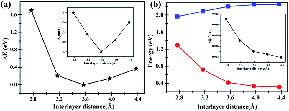 | ||
| Fig. 5 (a) The total energy of C2N/G heterostructure as a function of the interlayer distance and the zero of the energy scale is arbitrarily put at the equilibrium position. The inset shows the variation of the binding energy of C2N/G with the interlayer spacing. (b) Energy band gaps against the interlayer distance of C2N/G. The solid red circles denote the band gap openings of graphene, while the solid squares indicate the band gap of C2N. The inset presents the variation of the amount of transferred charges per C atom in graphene with the interlayer spacing. | ||
3.3. Perspectives
On one hand, band gap opening and tailoring in graphene is one of the most important and urgent research topics in the graphene applications, especially in single-layer graphene (SLG) FETs.3,25 In C2N/G heterostructures, the integrity of crystal structure and the charge mobility are preserved for graphene while its band gap is opened and tunable between 0.33 eV and 0.72 eV. Therefore, the C2N/G heterostructures are promising candidate channel materials for high performance SLG FETs.On the other hand, when integrated into the composites, the band structure characteristic of C2N is also preserved, as shown in Fig. 2(b)–(d). Fig. 5(b) indicates that the direct band gap is always in visible region when the interlayer spacing changes. What's more, though the CBM potentials of C2N in the heterostructures are lower than that of pristine monolayer C2N, they are still higher than the reduction potential of hydrogen, especially those of the C2N/G heterostructures at equilibrium spacing. And all of the VBM potentials are lower than the oxidation potential of H2O. The band edge alignments of pristine monolayer C2N and C2N in heterostructures are presented in Fig. 6. These results suggest that the C2N/G heterostructures can be used as metal-free alternatives of photocatalytic materials in water splitting.
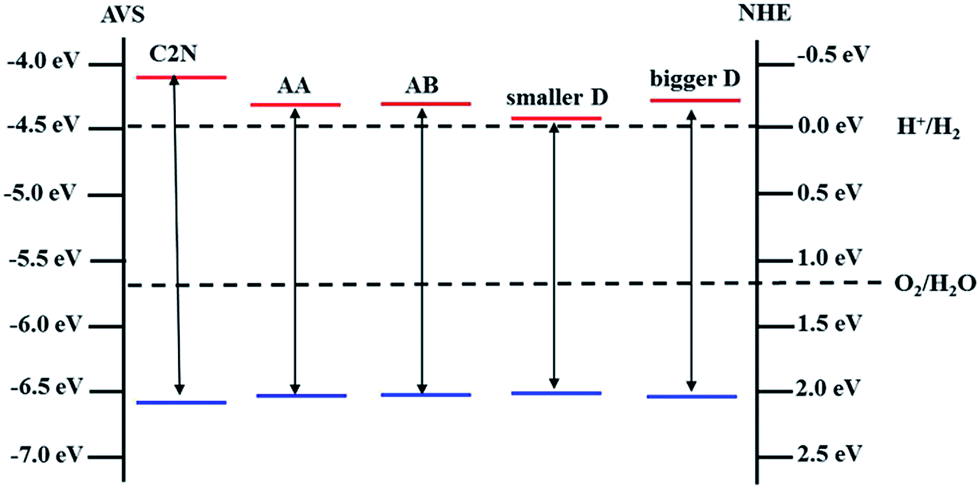 | ||
| Fig. 6 Band edge alignments of isolated monolayer C2N, C2N layer in C2N/G heterostructures with AA and AB stacking sequence at equilibrium spacing, C2N layer in C2N/G heterostructures (AB stacking) with smaller and bigger interlayer spacing, respectively. The dashed lines are water redox potentials. | ||
4. Conclusions
In summary, we investigated the structural and electronic properties of C2N/G heterostructures using hybrid functional DFT methods. The heterostructures are found to be stabilized through vdW interactions and possess electron transfer from graphene to C2N. A gap of about 0.40 eV is opened in graphene at equilibrium interlayer spacing, which is originated from the symmetry breaking. The interlayer interaction can induce tunable band gap between 0.33 eV and 0.72 eV in graphene by altering the interlayer spacing. We also find that the electronic properties of C2N, especially the direct band gap in visible region, are almost preserved. These results suggest that the C2N/G heterostructures can be used both as an electronic material for high-performance FETs and as a visible light responding photocatalyst for water splitting.Acknowledgements
This work was supported by NSFC, China (21225524, and 21475122 and 21205112) and the Department of Science and Techniques of Jilin Province (20150203002YY, 20150201001GX and SYHZ0006) and Chinese Academy of Sciences (YZ201354, YZ201355).References
- K. S. Novoselov, D. Jiang, F. Schedin, T. J. Booth, V. V. Khotkevich, S. V. Morozov and A. K. Geim, Proc. Natl. Acad. Sci. U. S. A., 2005, 102, 10451 CrossRef CAS PubMed
.
- K. S. Novoselov, V. Fal, L. Colombo, P. Gellert, M. Schwab and K. Kim, Nature, 2012, 490, 192 CrossRef CAS PubMed
- K. S. Novoselov, A. K. Geim, S. Morozov, D. Jiang, Y. Zhang and S. Dubonos, Science, 2004, 306, 666 CrossRef CAS PubMed
- S. Stankovich, D. A. Dikin, R. D. Piner, K. A. Kohlhaas, A. Kleinhammes, Y. Jia, Y. Wu, S. T. Nguyen and R. S. Ruoff, Carbon, 2007, 45, 1558 CrossRef CAS
- D. H. Long, W. Li, L. Ling, J. Miyawaki, I. Mochida and S. H. Yoon, Langmuir, 2010, 26, 16096 CrossRef CAS PubMed
- W. A. De Heer, C. Berger, M. Ruan, M. Sprinkle, X. Li, Y. Hu, Z. Baiqian, H. John and C. Edward, Proc. Natl. Acad. Sci. U. S. A., 2011, 108, 16900 CrossRef CAS PubMed
- D. Wang, L. Liu, W. Chen, X. Chen, H. Huang, J. He, Y.-P. Feng, A. Wee and D. Shen, Nanoscale, 2015, 7, 4522 RSC
- C.-M. Seah, S.-P. Chai and A. R. Mohamed, Carbon, 2014, 70, 1 CrossRef CAS
- C.-J. Shih, G. L. C. Paulus, Q. H. Wang, Z. Jin, D. Blankschtein and M. S. Strano, Langmuir, 2012, 28, 8579 CrossRef CAS PubMed
- F. Schwierz, J. Pezoldt and R. Granzner, Nanoscale, 2015, 7, 8261 RSC
- V. Apalkov and M. I. Stockman, Light: Sci. Appl., 2014, 3, e191 CrossRef CAS
- N. Papasimakis, S. Thongrattanasiri, N. I. Zheludev and F. G. de Abajo, Light: Sci. Appl., 2013, 2, e78 CrossRef
- F. Schwierz, Nat. Nanotechnol., 2011, 6, 135 CrossRef CAS PubMed
- A. H. Castro Neto, F. Guinea, N. M. R. Peres, K. S. Novoselov and A. K. Geim, Rev. Mod. Phys., 2009, 81, 109 CrossRef CAS
- A. Hashimoto, K. Suenaga, A. Gloter, K. Urita and S. Iijima, Nature, 2004, 430, 870 CrossRef CAS PubMed
- A. V. Krasheninnikov and F. Banhart, Nat. Mater., 2007, 6, 723 CrossRef CAS PubMed
- D. Wei, Y. Liu, Y. Wang, H. Zhang, L. Huang and G. Yu, Nano Lett., 2009, 9, 1752 CrossRef CAS PubMed
- M. Telychko, P. Mutombo, P. Merino, P. Hapala, M. Ondráček, F. C. Bocquet, J. Sforzini, O. Stetsovych, M. Vondráček, P. Jelínek and M. Švec, ACS Nano, 2015, 9, 9180 CrossRef CAS PubMed
- W. Strek, B. Cichy, L. Radosinski, P. Gluchowski, L. Marciniak, M. Lukaszewicz and D. Hreniak, Light: Sci. Appl., 2015, 4, e237 CrossRef CAS
- D. Elias, R. Nair, T. Mohiuddin, S. Morozov, P. Blake, M. Halsall, A. Ferrari, D. Boukhvalov, M. Katsnelson, A. K. Geim and K. S. Novoselov, Science, 2009, 323, 610 CrossRef CAS PubMed
- M. Jaiswal, C. H. Yi Xuan Lim, Q. Bao, C. T. Toh, K. P. Loh and B. Ozyilmaz, ACS nano, 2011, 5, 888 CrossRef CAS PubMed
- S. Y. Zhou, G.-H. Gweon, A. V. Fedorov, P. N. First, W. A. De Heer, D.-H. Lee, F. Guinea, A. H. C Neto and A. Lanzara, Nat. Mater., 2007, 6, 770 CrossRef CAS PubMed
- N. Kharche and S. K. Nayak, Nano Lett., 2011, 11, 5274 CrossRef CAS PubMed
- R. Decker, Y. Wang, V. W. Brar, W. Regan, H.-Z. Tsai, Q. Wu, W. Gannett, A. Zettl and M. F. Crommie, Nano Lett., 2011, 11, 2291 CrossRef CAS PubMed
- R. Quhe, J. Zheng, G. Luo, Q. Liu, R. Qin, J. Zhou, D. Yu, S. Nagase, W.-N. Mei, Z. Gao and J. Lu, NPG Asia Mater., 2012, 4, e6 CrossRef
- J. Mahmood, E. K. Lee, M. Jung, D. Shin, I.-Y. Jeon, S.-M. Jung, H.-J. Choi, J.-M. Seo, S.-Y. Bae, S.-D. Sohn, N. Park, J. H. Oh, H.-J. Shin and J.-B. Baek, Nat. Commun., 2015, 6, 1 Search PubMed
- B. Xu, H. Xiang, Q. Wei, J. Q. Liu, Y. D. Xia, J. Yin and Z. G. Liu, Phys. Chem. Chem. Phys., 2015, 17, 15115 RSC
- R. Zhang and J. Yang, 2015, arXiv preprint arXiv:1505.02768.
- R. Zhang, B. Lia and J. Yang, Nanoscale, 2015, 7, 14062 RSC
- H. K. Yu, K. Balasubramanian, K. Kim, J.-L. Lee, M. Maiti, C. Ropers, J. Krieg, J. Kern and A. M. Wodtke, ACS Nano, 2014, 8, 8636 CrossRef CAS PubMed
- S. Gottardi, K. Müller, L. Bignardi, J. C. Moreno-López, T. A. Pham, O. Ivashenko, M. Yablonskikh, A. Barinov, J. Björk, P. Rudolf and M. Stöhr, Nano Lett., 2015, 15, 917 CrossRef CAS PubMed
- J. P. Perdew, K. Burke and M. Ernzerhof, Phys. Rev. Lett., 1996, 77, 3865 CrossRef CAS PubMed
- G. Kresse and J. Hafner, Phys. Rev. B: Condens. Matter Mater. Phys., 1993, 47, 558 CrossRef CAS
- G. Kresse and D. Joubert, Phys. Rev. B: Condens. Matter Mater. Phys., 1999, 59, 1758 CrossRef CAS
- M. Dion, H. Rydberg, E. Schröder, D. C. Langreth and B. I. Lundqvist, Phys. Rev. Lett., 2004, 92, 246401 CrossRef CAS PubMed
- G. Román-Pérez and J. M. Soler, Phys. Rev. Lett., 2009, 103, 096102 CrossRef PubMed
- K. Lee, E. D. Murray, L. Kong, B. I. Lundqvist and D. C. Langreth, Phys. Rev. B: Condens. Matter Mater. Phys., 2010, 82, 081101 CrossRef
- J. Klimeš, D. R. Bowler and A. Michaelides, Phys. Rev. B: Condens. Matter Mater. Phys., 2011, 83, 195131 CrossRef
- J. Heyd, G. E. Scuseria and M. Ernzerhof, J. Chem. Phys., 2003, 118, 8207 CrossRef CAS
- I. Hamada and M. Otani, Phys. Rev. B: Condens. Matter Mater. Phys., 2010, 82, 153412 CrossRef
- Y.-C. Zhou, H.-L. Zhang and W.-Q. Deng, Nanotechnology, 2013, 24, 22570 Search PubMed
| This journal is © The Royal Society of Chemistry 2016 |