 Open Access Article
 This Open Access Article is licensed under a
 Creative Commons Attribution 3.0 Unported Licence
Accelerating research on novel photovoltaic materials
Thomas
Unold

Dept. Structure and Dynamics of Energy Materials, Helmholtz-Zentrum Berlin für Materialien und Energie, Hahn-Meitner Platz 1, 14109 Berlin, Germany. E-mail: unold@helmholtz-berlin.de
First published on 3rd June 2022
Abstract
The development of new materials typically takes many years or even decades. This has been particularly true for photovoltaic (PV) technologies, which require control of defects on the parts-per-million-level and consist of relatively complex device structures comprising many elements and interfaces between materials. This means that optical and electronic properties can be difficult to pin down, and also heavily depend on the details of processing. Although processing often varies from lab to lab, complete protocols are rarely reported or accessible. It is suggested that the development of novel photovoltaic materials could be greatly stimulated if information and data is more openly shared, and FAIR data management is implemented in the research community. Massive storage of research results with rich metadata in an FAIR-compliant open-access database is envisioned as a great potential for acceleration in emerging PV materials development.
Introduction
For many years thin film photovoltaics has carried the promise of providing an inexpensive and versatile source of electricity, through its low material usage and flexibility in design as well as in application. Using multinary compounds enables a wide range of optical and electronic properties that can be further tuned by alloying. Some processing techniques employed in thin film photovoltaics such as magnetron sputtering are established, scalable coating techniques and thus in principle compatible with the architectural glass industry, which is a huge global market. Also, flexible substrates can be employed, enabling low foot-print roll-to-roll technologies. Finally, the theoretical efficiency potential of thin film inorganic photovoltaics is as large or even exceeds crystalline silicon, depending on the band gap of the absorber material.Despite all of these obvious advantages, thin film photovoltaic technology has struggled to keep up with wafer-based crystalline silicon PV technology, with respect to module efficiency, as well as market share.1,2 In fact, currently only CdTe-based thin film solar cells have been able to defend their position in the market, with close to 19% module efficiency and being cost competitive with or lower than silicon PV.3 Among the emerging inorganic thin film PV materials, the kesterite Cu2ZnSnSe4 has been the most actively researched, but so far did not reach sufficiently high efficiencies.4 The benchmark for photoconversion efficiency in photovoltaic materials has been a moving target during the last 20 years. When research on amorphous silicon peaked in the 1990s, a 10% device efficiency was considered sufficient for commercial success in the PV market. Indeed, commercial amorphous silicon modules did reach the stabilized 10% efficiency level in the late 90 s.5 However, due to the drastically decreased cost of PV modules and significant efficiency increases of crystalline silicon technology during the last 10–20 years (and thus the increased importance of balance of system costs), the target efficiency has now moved up to about 20%, which is obviously much harder to achieve.
The more established PV technologies, silicon, chalcopyrite, cadmium–telluride, III–V semiconductors now have all demonstrated – at least on small area-efficiencies above 20%.1 These achievements, however, were not reached overnight, but as a result of 30–40 years of research. This creates increasing pressure on research in novel, emerging photovoltaic materials and device concepts to be fast in solving problems and delivering high efficiencies. Looking at the current state of research raises doubts whether a continuation of the current research paradigm will be adequate to address this situation. Possible routes and paradigm shifts for accelerating research in emerging PV materials will be discussed in this publication.
Results and discussion
The evolution of cell conversion efficiencies for some more established and some emerging PV materials are shown in Fig. 1.1,6–8 Looking at the evolution of CIGSe and CdTe cell performance it can be seen that there have been extended periods with little progress followed by periods with significant increases in efficiency. These more productive periods can usually be associated with the effect of break-through discoveries, such as the incorporation of sodium or potassium in CIGSe, or the establishment of CdCl2 treatment in CdTe.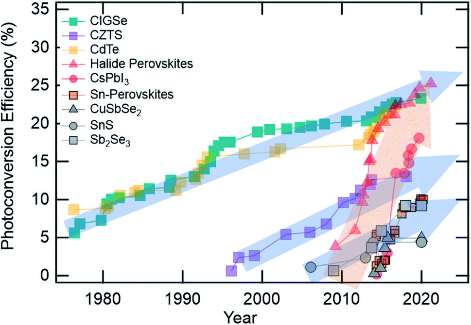 | ||
| Fig. 1 Evolution of cell performance for a variety of thin film photovoltaic materials. Light arrows are guides to the eye. | ||
Comparing the development of kesterite (CZTS) photovoltaics to the progress of CIGSe and CdTe it can be seen that the annual increase in efficiency is not so different, but shifted in time, because kesterite research started about 20 years later. Extrapolating the rate of efficiency increase to the future predicts that 20% small area efficiency could be reached for kesterites around 2028. Of course, it is possible that due to inherent material limits or limits imposed by the necessary device structure this efficiency value cannot be reached. Such a material limit could be the too low formation energies (and therefore abundant presence) of deep defects with large capture cross-sections for charge carriers, as has been recently predicted and discussed for kesterite-type materials.9 However, strategies to overcome the effect of low defect formation energies also have been proposed such that it will be assumed here that 20% device efficiency can be reached by the combined effort of the research community at least for the band gap range between 1 eV to 1.8 eV, which would require reasonable charge carrier lifetimes (see Discussion below).
Other emerging PV materials, such as SnS or Sb2Se3, currently show low efficiencies (<10%), however, with an overall similar rate of efficiency increase as the previously discussed technologies. Thus it could be expected that 20% may be reached for these technologies in about 20 years time, if all current and future obstacles can be overcome. It can also be observed in Fig. 1 that one class of emerging PV materials has demonstrated a significantly larger rate of efficiency increase, namely halide perovskites (HaP). As indicated by the red symbols, this applies to both hybrid as well as inorganic Pb-based halide perovskites, with efficiencies above 20% reached within a time-period of 10 years. This raises several questions with respect to research in thin film inorganic PV:
(1) Is the current rate of progress in inorganic thin film PV sufficient to provide viable alternatives to established PV technology?
(2) Why has progress in halide perovskites been so fast ?
(3) How could research in inorganic PV be accelerated?
I propose that question 1 should be clearly answered with no. It is very unreasonable to believe that we can allow a 20–30 year time horizon for the development of new PV materials in PV, if we expect them to have a real impact in providing sustainable electricity and in mitigating the climate problem. Regarding the second question 2, there are likely several reasons for the success of halide perovskite technology. At least Pb-based halide perovskites seem to be unusually defect tolerant materials, enabling very long minority carrier lifetimes up to tens of microseconds.10,11 Also, various organic and inorganic electron and hole transporting contact layers exist that have close to ideal band lineups with the HaP absorber layer.12 Lastly, hybrid halide perovskites can be solution-processed at low temperature, with only low cost equipment necessary.13 This enables many labs around the world to participate in a kind of crowd-research effort. The number of groups participating and the number of devices fabricated within the last ten years of research in HaP is astounding. On top of this, many processing variants have been trialed and successful recipes have been relative openly shared, in some cases to great detail.14
Compared to this huge research community, the number of groups working on alternative (inorganic) emerging PV can be considered quite modest. This leads into the discussion of question 3, how PV research in general could be accelerated. I believe there are several possibilities, opportunities and necessities to accelerate research and development of emerging PV materials. First, experiments could be accelerated by using so-called combinatorial synthesis and high-throughput analysis methods.15–17 This allows to establish phase diagrams and structure–property-function relationships much faster than by commonly used ‘one sample at a time’ methods. By combining charge transport layers, buffer layers, absorber layers in a systematic combinatorial approach, the parameter space of possible device configurations can be explored much more rapidly and with better statistics than using linear, consecutive, one-sample-at-a-time approaches.18
Second, there should be a stronger focus on validating or disproving hypotheses.19 My observation is that research in emerging materials is often scattered into individual approaches and research branches, and theories and hypothesis are often developed without much attention to previous work or hypotheses. This often leads to the coexistence of (sometimes contradicting) theories or models, which describe local maxima in device efficiency without providing a clear pathway to solving the big problem. In order to approve or disprove hypotheses, it would be necessary to state clear hypotheses in publications. This is sometimes done, but also often remains diffuse. To test a hypothesis requires a high degree of reproducibility at least in synthesis, which in turn requires that processing and experimental conditions are stated in as much detail as possible. However, most publications currently do not provide sufficient level of detail in the description of synthesis (with notable exceptions e.g. ref. 14). This lack of sufficient synthesis details in publications may sometimes be intended to protect proprietary information, or because it is not deemed important for the community.
Round-robin strategies can be used both in synthesis and experiment to combine expertise between different research groups. As such characterization round-robin experiments often yield significant deviations from lab to lab, they can be used to establish confidence bounds on materials properties, and also be used to establish best-practices in the community.20 As an example, we recently showed in a interlab-collaboration between 15 groups how mobility measurements by Thz spectroscopy and microwave conductivity characterization of halide perovskites can yield significant differences despite being performed on identical samples.21
Third, we urgently need digitization of data, in the sense that data are made digitally available, and conform to the FAIR principles. The FAIR data concept was introduced by Wilkinson et al. in 2016 and proposed basic principles to promote the reuse of scholarly data, both by machines and individuals.22 The acronym FAIR stands for the guiding principles: findable, accessible, interoperable and reusable (see Table 1). Although the FAIR data principles have received considerable attention in the recent years, currently almost no FAIR data are in existence in photovoltaic materials research. At present, the majority of material science research still proceeds in the long-established work flow of (1) collecting data on local computers, (2) selecting certain ‘best’ data to support a message or model, (3) reporting data/results/models in form of graphs or sometimes tables in scientific publications and (4) keeping or archiving the majority of data on the local computer. Most of the data and also metadata are not shared or made accessible and will be lost for further research. This in particular applies to negative research results, which are rarely shared with the community, but could contribute to future advances in a particular field.23
| Principle | Meaning | Emerging PV research |
|---|---|---|
| Findable | Data are linked to persistent unique identifier, decorated with rich metadata | PV materials database with rich metadata, data sets labeled with PIDs |
| Accessible | Data are stored sustainably and can be accessed and transferred digitally | Either centralized data storage of data or persistent accessible storage at institution level |
| Interoperable | Data formats, meaning and units are defined | Thesaurus, ideally photovoltaics ontology |
| Reusable | Licensed users can reuse data for further research | Ideally open access, at least for publicly funded research |
Although publications are nowadays almost exclusively digital, their usage is mainly analog, in the sense that their contents is not machine-actionable. To give an example, in order to further analyze a JV or EQE curve displayed in a publication, the reader has to first digitize them, before being able to digitally process the data. Although data of course could be also obtained by exchanging mails with the corresponding author, this can be a tedious and time-consuming process, and with increasing time between publication and request this may lead to problems with locating and contextualizing the data.
Photovoltaic device efficiency tables vs. databases
Small and larger steps can be taken to move emerging PV materials research toward FAIR data principles. There are currently several publications that include solar cell efficiency tables,1 with two publications dedicated to emerging PV materials,6,7 one of them exclusively to inorganic emerging PV materials.7 These publications include overview graphs, discussion and tables. However, currently the publications are completely analog, in the sense that they provide no digital, machine-readable form of the data displayed. In order to use the data in these publications, they have to be manually extracted and digitized. Also, the tables contain a very incomplete set of information and metadata about the devices: in ref. 6 the absorber material, band gap, efficiency, open-circuit voltage, short circuit current are listed; in ref. 7 absorber material, band gap, efficiency, Voc, Jsc, FF, device structure, cell area, and certifying lab are listed. This can serve as an orientation of what the state-of-the-art in a certain technology is, with respect to photoconversion efficiency, but it does not allow to extract further information on the status in the field, as for example the reproducibility, about synthesis approaches that work or that do not work, and about identification of limiting factors of the electronic quality or the potential for photoconversion.To make much larger quantities of data available, the research community should move toward sharing data in databases. Although there have been a significant number of material science databases or data repositories in operation, e.g. the Inorganic Crystal Structure Database (ICSD) (https://icsd.fiz-karlsruhe.de/), the crystallography open database (https://www.crystallography.net), the Pauling File (https://paulingfile.com/), the European Open Science Cloud (https://eosc-portal.eu/), Figshare (https://figshare.com/), Zenodo (https://zenodo.org) and others, they often are not easy to use and/or behind a pay-wall, or extremely heterogeneous. In many cases they typically contain some material properties but no complete and linked data sets. As a notable exception, NREL has been providing an open access ‘High Throughput Experimental Materials Database’,24 which however, currently only contains NREL data, and does not include solar cell devices. Databases fully complying with the fair principles have been established for computational material science data, for example the materialsproject25 (https://materialsproject.org/) and the Novel Materials Discovery Database26 (https://www.nomad-coe.eu/).
With regard to solar cell devices, there have been a few efforts launched recently. The emerging PV database (https://emerging-pv.org/data/) contains device performance data (efficiency, Voc, Jsc, FF, Eg, stability) of emerging PV data and links to publications. Although this goes into the right direction, it would be desirable to provide more data/metadata for each dataset. How this can play out can be seen in the recently launched database on halide perovskite solar cells, the ‘perovskite database project’.27 For this database, the complete halide perovskite (HaP) literature containing solar cell data was digitized in a collaborative effort of more than 100 coauthors, and made available in an open-access database (https://perovskitedatabase.com/). In contrast to efficiency tables, or the NREL chart, the database contains not only champion device but all solar cell device data on HaP (>40![[thin space (1/6-em)]](https://www.rsc.org/images/entities/char_2009.gif) 000) published so far. It comprises not only JV-characteristics and the bandgap, but up to 400 additional metadata. All metadata are digitally accessible and can be used for visualization, analysis and data mining. I use the terminology metadata here in a broader sense, which includes not only descriptions such as sample size, device structure, processing details, but also material parameters derived from original (raw) data such as bandgap, efficiency, composition.
000) published so far. It comprises not only JV-characteristics and the bandgap, but up to 400 additional metadata. All metadata are digitally accessible and can be used for visualization, analysis and data mining. I use the terminology metadata here in a broader sense, which includes not only descriptions such as sample size, device structure, processing details, but also material parameters derived from original (raw) data such as bandgap, efficiency, composition.
The digital storage of a large number of device or material-correlated metadata enables researchers to probe the state-of-the-art, to study approaches that did not yield record results, and search for correlation between certain configurations and processing steps. As an example, in Fig. 2 the published efficiencies of inorganic halide perovskite as a function of publication year are shown using box plots. The data are further distinguished by device structure, either p–i–n or n–i–p. It can be seen that in 2019 some of the best devices were in p–i–n geometry, while in 2020 the n–i–p devices showed better performance. The data can be easily further screened, for example for the exact, type of back and front contact used, for the choice of solvents in processing, hysteresis measurements and more.28
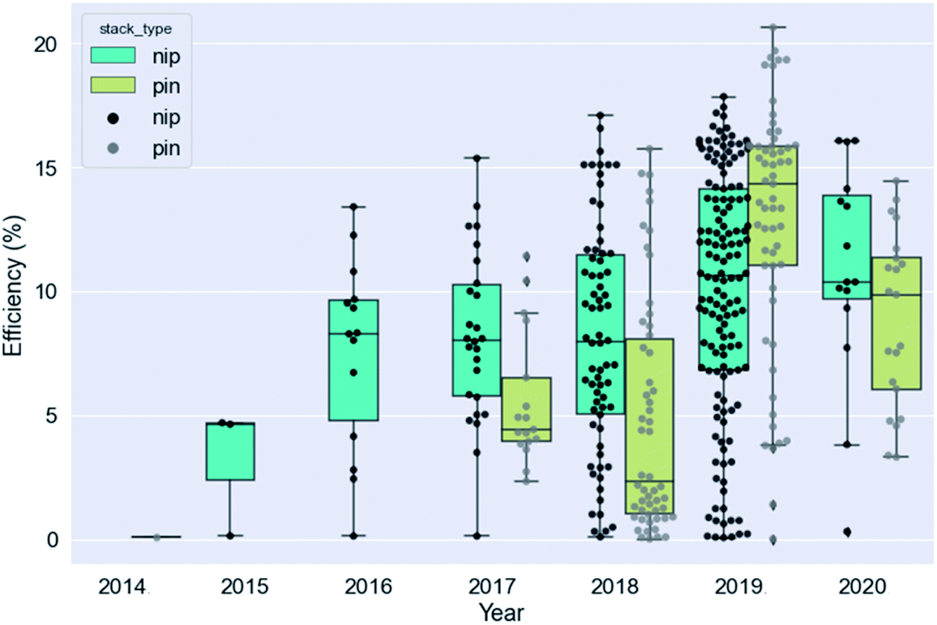 | ||
| Fig. 2 Efficiency values vs. publication year of various inorganic halide perovskites, separated by device configuration. Data obtained from https://perovskitedatabase.com. | ||
Semantics of PV data
In order to accelerate research in emerging PV materials it would be advantageous to share, archive and make available an as large set of metadata and data as possible. If data are properly labeled and decorated with rich metadata, the database will be searchable by smart query tools. In order to facilitate the understanding of data both for researchers and computers, the database should be embedded in a semantic framework. Such semantic framework, defining the meaning of the data and metadata, and the logical relations between them has been established for many fields using taxonomies and formal ontologies.29 Establishing ontologies in research field has the advantage to provide definitions, synonyms and relations between classes, which allows the inference of knowledge by machine learning.30 It also deals with the problem of ambiguous labeling of metadata, which complicate searches and the ability to infer knowledge. An ontology encompasses a taxonomy of concepts and their logical relations with each other, maps hierarchies and synonyms in a formalized structure, e.g. using the OWL web ontology language.31 Recently there have been large efforts by the European Materials Modelling Council to establish and define a common ontological approach for materials research, the standard European Materials Modelling Ontology (EMMO), which can serve as a top level ontology for more specific domain ontologies (https://emmc.info/emmo-info/).From JV results to descriptors
In the ideal research world all data and metadata of processes, materials and devices would recorded, saved and made available to the research community. However, this seems unreasonable at the present stage, and thus it may be worth contemplating about some material parameters that could significantly accelerate research if they would be reported as standard practice.32 As discussed in a previous section, efficiency tables and reviews often list only the most basic parameters measured on solar cells, such as JV-results (4 values), sometimes also EQE-data and bandgap of the material. The JV parameters have been generally used as a figure of merit for PV devices in the community. However, figures of merit that rely on full devices are problematic for emerging PV materials, since materials as well as devices are usually far from ideal. Hence low efficiencies found for these devices can be caused by various different problems, from low lifetime, interface recombination, lack of suitable band line-up with transport layers, shunt resistance, high series resistance and more. Research could significantly benefit if larger sets of results on material parameters are investigated and reported as standard procedure, including details on processing routes. Some material properties can be measured for partial device stacks or bare absorbers, and thus would allow a better classification, error search, process and material tuning to guide the search for better devices.For a classical semiconductor material properties can be classified into 2 groups: such that are fundamental and are not expected to change by processing, and such that depend on processing and can be optimized. The first group includes band gap, absorption coefficient, intragrain carrier mobilities, electron affinity, effective masses, radiative recombination coefficient. The second group includes carrier lifetime, charge carrier density, Fermi-level position, photoluminescence quantum efficiency, defect densities, band tails. For a multinary polycrystalline material the first group of fundamental parameters can become less fixed and depend on processing, e.g. if the absorption edge becomes very broad such that the definition of the band gap becomes challenging,33 or if carrier transport is limited by grain boundary scattering.
In the following some parameters that i deem essential to characterize and collect in a materials database in emerging PV materials research are proposed and illustrated: carrier lifetime, doping density, photoluminescence quantum yield, absorption coefficient and carrier mobilities, ionization potential. In order to illustrate the importance of these parameters, i have performed model drift-diffusion calculations using SCAPS1D,34 for a hypothetical material with perfectly aligned and highly selective electron and hole contacts (Fig. 3a). The role of the band gap and carrier lifetime for conversion efficiency of PV devices is well-known and shown for a 1 μm thick model thin film device with hole (doping) density of 1015 cm−3 and charge carrier mobilities of 50 cm2 V−1 s−1 in Fig. 3b. The predicted device efficiency peaks at an optimum bandgap between 1.3–1.6 eV, where the larger band gaps are preferred for low lifetime and the smaller band gaps are preferred for the high lifetime materials. The figure also shows the best reported device efficiencies for CIGSe, CdTe, HaP and CZTSe, indicating “effective” carrier lifetimes between 1 ns to 1 μs for the different materials, in fact consistent with reports in the literature.21,35–37
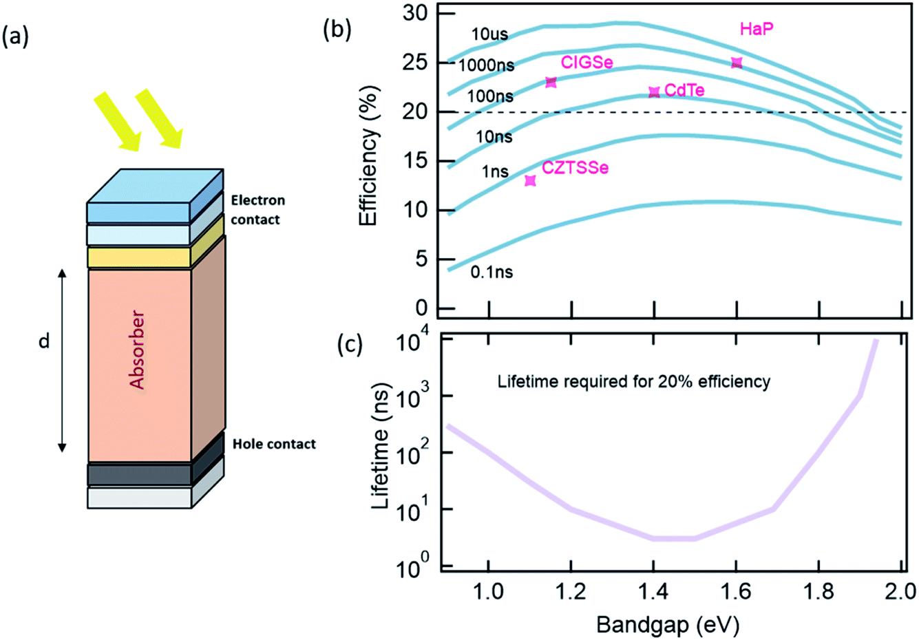 | ||
| Fig. 3 (a) Schematic of photovoltaic device simulated with drift-diffusion model SCAPS1D. (b) Simulated efficiency as a function of bandgap for a device with ideal contacting layers and parametrized minority carrier lifetime. Na = 1015 cm−3, μn, μp = 50 cm2 V−1 s−1, d = 1 μm, krad = 2 10−11 cm3 s−1. Stars indicate reported best device efficiencies.1 (c) Minimum effective carrier lifetime required for 20% device efficiency for these device parameters. | ||
It is interesting to evaluate what carrier lifetime would be needed for a 20% device efficiency, under these material/device assumptions, which is shown in Fig. 3c. It can be seen that the required carrier lifetime varies strongly for different material band gaps, with a minimum value of 3 ns found for a bandgap between 1.4–1.5 eV.
The effect of doping and lifetime on a model device with a bandgap of 1.1 eV is shown in Fig. 4a and b. It can be seen that efficiency and open-circuit voltage monotonically increase with effective lifetime (here resembling an effective lifetime for all non-radiative recombination in the device), but that the dependence of efficiency on the doping density is more complex. Although the open-circuit voltage increases monotonically with doping, the efficiency can actually decrease for higher doping, if the effective lifetime in the device is below 3 ns. This illustrates that in addition to bandgap, lifetime and doping are 2 important material descriptors defining the electronic properties of thin film PV devices and conversion efficiency.
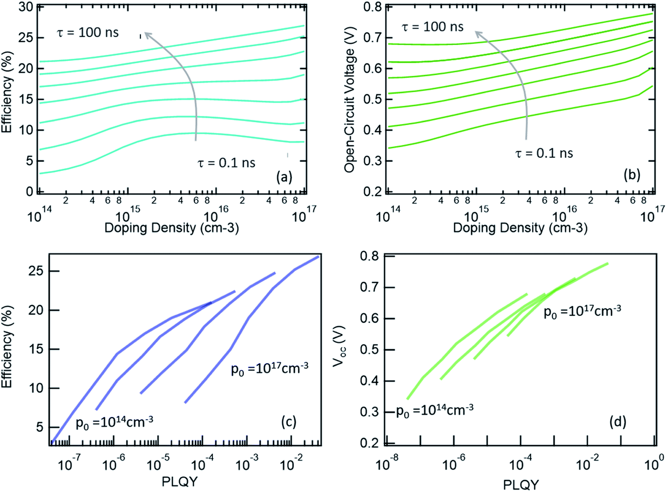 | ||
| Fig. 4 (a) Simulated device efficiency as a function of doping density for a 1.1 eV bandgap material, for different carrier lifetimes. (b) Simulation of open-circuit voltage as a function of doping density for a 1.1 eV bandgap material, for different carrier lifetimes. (c) Simulated open-circuit voltage as a function of PL quantum yield (d) open-circuit voltage as a function of PL quantum yield, for different doping densities. | ||
However, both material properties can be difficult to characterize for thin film materials. Time-resolved photoluminescence is commonly used to determine the carrier lifetime, but can be distorted by carrier trapping and retrapping,37 carrier separation,38 the effect of surface recombination and degradation in unfinished devices.39 Carrier densities can be determined by Hall measurements, which however requires thin films without back contact, admittance-based techniques. For the latter technique the determination of correct carrier densities can be hampered by back contact barriers, deep defects, carrier depletion and carrier injection.40
A material property that depends on both carrier lifetime and carrier density is the photoluminescence quantum yield (PLQY), which can be measured on absorbers, partial stacks and full devices.41,42 To illustrate the usefulness of PLQY as a descriptor for thin film device performance, the simulated efficiency and open-circuit voltage is shown as a function of PLQY and carrier density in Fig. 4c and d. It can be seen that both open-circuit voltage and efficiency increase monotonically with increasing PLQY. Whereas the open-circuit voltage depends only modestly on carrier density for a fixed PLQY value, this dependence is stronger for the efficiency. As an example, for a PLQY = 10−5 (corresponding to the best kesterite solar cells43), the expected efficiency for a doping density of 1016, 1015, 1014 cm−3 would be 11, 16 and 17%, respectively. This is due to the fact that for low doping densities, a large PLQY is due to long carrier lifetimes, whereas for high doping densities the PLQY can be high despite low carrier lifetimes.41 Also, ideal selective contacts are assumed in simulation, whereas in a real device current as well as voltage losses can occur due to non-ideal contacts. As also can be seen in Fig. 4b, the most direct relationship is obtained between PLQY and the quasi-Fermi level splitting in the material or device. PLQY measurements on bare absorber layers show the open-circuit voltage potential of a material, whereas PLQY measurements on devices reveal the effects of additional recombination occurring at the charge-transport and contacting layers.42 Additionally, energetically misaligned contact layers can reduce the externally measured Voc of a device, when compared to the internal voltage estimated from PLQY.36,44
Next the effect of the absorption strength and carrier mobility on device performance is illustrated. Assuming an ideal direct band gap absorption coefficient given by 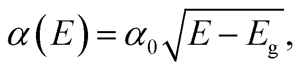 the effect of varying the absorption strength 104 cm−1 eV−0.5 < α0 < 105 cm−1 eV−0.5 on device efficiency is shown in Fig. 5a. It can be seen that in particular for devices with short diffusion lengths < 400 nm, the predicted efficiency decreases strongly if α0 drops below 4 × 104 cm−1 eV−0.5. For longer diffusion lengths of 1000 nm shown in blue curves, the efficiency can be slightly boosted by increasing the device thickness, but this is does not help for the smaller diffusion lengths. The absolute strength of absorption not only has a strong effect on device performance, but of course also strongly influences the outcome of device simulations, and thus should be considered an important descriptor for PV performance.
 | ||
| Fig. 5 (a) Simulated Efficiency as a function of absorption strength. Solid lines indicate a device thickness of 1 micrometer and dashed lines a thickness of 2 micrometers. (b) Simulated efficiency as a function of electron mobility for different hole mobilities (0.1–100 cm2 V−1 s−1). A carrier lifetime of 10 ns is assumed. The vertical grey line indicates the typical carrier mobility arising from grain boundary scattering. | ||
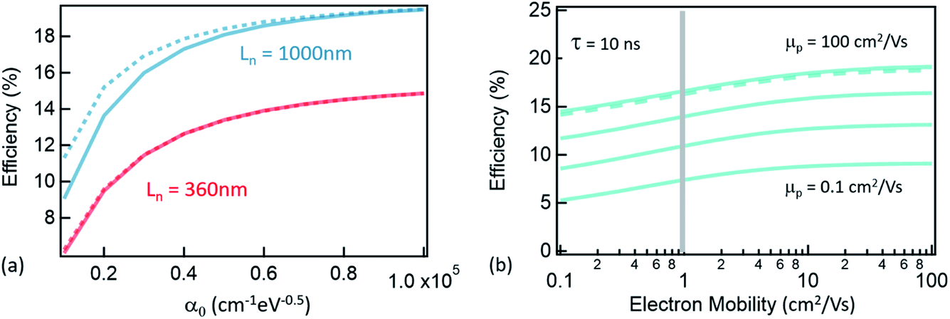
Fig. 5b shows the predicted device efficiency for different intragrain carrier mobilities, assuming a carrier lifetime τ = 10 ns, and doping density of 1015 cm−3 and α = 6.8 1044 cm−1 (the latter parameter was used in all simulations shown in Fig. 3 and 4). Note that the mobility here denotes an effective mobility, which could be either intergrain if transport proceeds across several grains, or intragrain if grain sizes are sufficiently large. It can be seen that the predicted efficiency decreases significantly if at least one of the carrier mobilities drops below 10 cm2 V−1 s−1, which can be easily the case for small-grain materials, or materials with strong carrier localization.45–47
Since the dependency of device performance on material properties are multidimensional, the results shown in Fig. 3 and 4 only offer a snapshot and obviously cannot provide all necessary information to analyze and estimate the PV potential of a certain material class, or a specific device fabrication process in particular. However, the discussion shows that in order to efficiently guide research and to be able to optimize devices rapidly, information on more material parameters than JV characteristics and band gap are needed. If these are reported, saved as FAIR data objects together with device performance data and detailed processing information, we can envision the creation of interoperable databases, which would be extremely useful for the accelerated advancement of emerging PV materials research. Data heterogeneity is still a big problem with the current existence of specialized databases, which poses a significant obstacle for uploading and downloading data for research purposes. The German FAIRmat project, which started in 2021, has the goal to setup an easy-to-use open-access database structure for the physical chemistry of solids.48 The database framework will integrate data from theory, synthesis, experiment and application use cases, such photovoltaic device and intends to provide low entry level tools for uploading, downloading and visualization of data. This platform could become a possible data infrastructure solution for acceleration of emerging PV materials as discussed in this publication. The data shown in this publication will be made available on https://zenodo.org/record/7030982.
Summary
In this manuscript i have made the case that the research on novel photovoltaic material should and also could be accelerated manyfold, if research data including synthesis procedures, material properties and device characteristics are shared openly and according to FAIR principles. An evaluation of the state of research and publication culture shows that the potential of digitization is currently not sufficiently exploited. It is proposed that research data are made available in databases complying with FAIR principles, and that the community should work toward establishing a semantics in form of ontologies to make data interoperable and machine actionable. To accelerate the development of novel PV absorber materials, it is proposed that in addition to the commonly employed JV-benchmarking, more focus is set on establishing and reporting descriptors such as (1) absorption coefficient (2) carrier density (3) carrier lifetime (4) photoluminescence quantum yield (5) (minority) charge carrier mobility.Conflicts of interest
There are no conflicts to declare.Acknowledgements
This work has been supported by the Helmholtz-Association Impuls and Network funding (Autoperosol Project), by the DFG-funded NFDI-project Fairmat and by the Horizon2020 research and innovation programme under grant agreement no. 952982 (Custom-Art project).References
- M. A. Green, E. D. Dunlop, J. Hohl-Ebinger, M. Yoshita, N. Kopidakis and X. Hao, Prog. Photovoltaics Res. Appl., 2022, 30, 3–12 CrossRef.
- Photovoltaics Report – Fraunhofer ISE, https://www.ise.fraunhofer.de/en/publications/studies/photovoltaics-report.html, accessed 24 April 2022 Search PubMed.
- G. M. Wilson, M. Al-Jassim, W. K. Metzger, S. W. Glunz, P. Verlinden, G. Xiong, L. M. Mansfield, B. J. Stanbery, K. Zhu, Y. Yan, J. J. Berry, A. J. Ptak, F. Dimroth, B. M. Kayes, A. C. Tamboli, R. Peibst, K. Catchpole, M. O. Reese, C. S. Klinga, P. Denholm, M. Morjaria, M. G. Deceglie, J. M. Freeman, M. A. Mikofski, D. C. Jordan, G. Tamizhmani and D. B. Sulas-Kern, J. Phys. D. Appl. Phys., 2020, 53, 493001 CrossRef CAS.
- S. Giraldo, Z. Jehl, M. Placidi, V. Izquierdo-Roca, A. Pérez-Rodríguez and E. Saucedo, Adv. Mater., 2019, 31, 1806692 CrossRef PubMed.
- B. Stannowski, O. Gabriel, S. Calnan, T. Frijnts, A. Heidelberg, S. Neubert, S. Kirner, S. Ring, M. Zelt, B. Rau, J. H. Zollondz, H. Bloess, R. Schlatmann and B. Rech, Sol. Energy Mater. Sol. Cells, 2013, 119, 196–203 CrossRef CAS.
- O. Almora, D. Baran, G. C. Bazan, C. Berger, C. I. Cabrera, K. R. Catchpole, S. Erten-Ela, F. Guo, J. Hauch, A. W. Y. Ho-Baillie, T. J. Jacobsson, R. A. J. Janssen, T. Kirchartz, N. Kopidakis, Y. Li, M. A. Loi, R. R. Lunt, X. Mathew, M. D. McGehee, J. Min, D. B. Mitzi, M. K. Nazeeruddin, J. Nelson, A. F. Nogueira, U. W. Paetzold, N. G. Park, B. P. Rand, U. Rau, H. J. Snaith, E. Unger, L. Vaillant-Roca, H. L. Yip and C. J. Brabec, Adv. Energy Mater., 2021, 11, 2102526 CrossRef CAS.
- A. Zakutayev, J. D. Major, X. Hao, A. Walsh, J. Tang, T. K. Todorov, L. H. Wong and E. Saucedo, J. Phys. Energy, 2021, 3, 032003 CrossRef CAS.
- Best Research-Cell Efficiency Chart, Photovoltaic Research, NREL, https://www.nrel.gov/pv/cell-efficiency.html, accessed 24 April 2022 Search PubMed.
- S. Kim, J. A. Márquez, T. Unold and A. Walsh, Energy Environ. Sci., 2020, 13, 1481–1491 RSC.
- W. J. Yin, T. Shi and Y. Yan, Appl. Phys. Lett., 2014, 104, 063903 CrossRef.
- E. Gutierrez-Partida, H. Hempel, S. Caicedo-Dávila, M. Raoufi, F. Peña-Camargo, M. Grischek, R. Gunder, J. Diekmann, P. Caprioglio, K. O. Brinkmann, H. Köbler, S. Albrecht, T. Riedl, A. Abate, D. Abou-Ras, T. Unold, D. Neher and M. Stolterfoht, ACS Energy Lett., 2021, 6, 1045–1054 CrossRef CAS.
- Q. D. Ou, C. Li, Q. K. Wang, Y. Q. Li and J. X. Tang, Adv. Mater. Interfaces, 2017, 4, 1600694 CrossRef.
- W. A. Dunlap-Shohl, Y. Zhou, N. P. Padture and D. B. Mitzi, Chem. Rev., 2019, 119, 3193–3295 CrossRef CAS PubMed.
- M. Saliba, J. P. Correa-Baena, C. M. Wolff, M. Stolterfoht, N. Phung, S. Albrecht, D. Neher and A. Abate, Chem. Mater., 2018, 30, 4193–4201 CrossRef CAS.
- H. Koinuma and I. Takeuchi, Nat. Mater., 2004, 3, 429–438 CrossRef CAS PubMed.
- Y. T. Huang, S. R. Kavanagh, D. O. Scanlon, A. Walsh and R. L. Z. Hoye, Nanotechnology, 2021, 32, 132004 CrossRef CAS PubMed.
- A. Ludwig, NPJ Comput. Mater., 2019, 5, 70 CrossRef.
- D. P. Tabor, L. M. Roch, S. K. Saikin, C. Kreisbeck, D. Sheberla, J. H. Montoya, S. Dwaraknath, M. Aykol, C. Ortiz, H. Tribukait, C. Amador-Bedolla, C. J. Brabec, B. Maruyama, K. A. Persson and A. Aspuru-Guzik, Nat. Rev. Mater., 2018, 3, 5–20 CrossRef CAS.
- K. Popper, Realism and the Aim of Science: from the Postscript to the Logic of Scientific Discovery, Taylor and Francis, 2013 Search PubMed.
- R. L. Z. Hoye, P. Schulz, L. T. Schelhas, A. M. Holder, K. H. Stone, J. D. Perkins, D. Vigil-Fowler, S. Siol, D. O. Scanlon, A. Zakutayev, A. Walsh, I. C. Smith, B. C. Melot, R. C. Kurchin, Y. Wang, J. Shi, F. C. Marques, J. J. Berry, W. Tumas, S. Lany, V. Stevanović, M. F. Toney and T. Buonassisi, Chem. Mater., 2017, 29, 1964–1988 CrossRef CAS.
- H. Hempel, T. J. Savenjie, M. Stolterfoht, J. Neu, M. Failla, V. C. Paingad, P. Kužel, E. J. Heilweil, J. A. Spies, M. Schleuning, J. Zhao, D. Friedrich, K. Schwarzburg, L. D. A. Siebbeles, P. Dörflinger, V. Dyakonov, R. Katoh, M. J. Hong, J. G. Labram, M. Monti, E. Butler-Caddle, J. Lloyd-Hughes, M. M. Taheri, J. B. Baxter, T. J. Magnanelli, S. Luo, J. M. Cardon, S. Ardo and T. Unold, Adv. Energy Mater., 2022, 12, 2102776 CrossRef CAS.
- M. D. Wilkinson, M. Dumontier, Ij. J. Aalbersberg, G. Appleton, M. Axton, A. Baak, N. Blomberg, J. W. Boiten, L. B. da Silva Santos, P. E. Bourne, J. Bouwman, A. J. Brookes, T. Clark, M. Crosas, I. Dillo, O. Dumon, S. Edmunds, C. T. Evelo, R. Finkers, A. Gonzalez-Beltran, A. J. G. Gray, P. Groth, C. Goble, J. S. Grethe, J. Heringa, P. A. C. t Hoen, R. Hooft, T. Kuhn, R. Kok, J. Kok, S. J. Lusher, M. E. Martone, A. Mons, A. L. Packer, B. Persson, P. Rocca-Serra, M. Roos, R. van Schaik, S. A. Sansone, E. Schultes, T. Sengstag, T. Slater, G. Strawn, M. A. Swertz, M. Thompson, J. Van Der Lei, E. Van Mulligen, J. Velterop, A. Waagmeester, P. Wittenburg, K. Wolstencroft, J. Zhao and B. Mons, Sci. Data, 2016, 3, 1–9 Search PubMed.
- P. Raccuglia, K. C. Elbert, P. D. F. Adler, C. Falk, M. B. Wenny, A. Mollo, M. Zeller, S. A. Friedler, J. Schrier and A. J. Norquist, Nature, 2016, 533, 73–76 CrossRef CAS.
- A. Zakutayev, N. Wunder, M. Schwarting, J. D. Perkins, R. White, K. Munch, W. Tumas and C. Phillips, Sci. Data, 2018, 5, 180053 CrossRef PubMed.
- A. Jain, S. P. Ong, G. Hautier, W. Chen, W. D. Richards, S. Dacek, S. Cholia, D. Gunter, D. Skinner, G. Ceder and K. A. Persson, APL Mater., 2013, 1, 011002 CrossRef.
- C. Draxl and M. Scheffler, MRS Bull., 2018, 43, 676–682 CrossRef.
- T. J. Jacobsson, et al., Nat. Energy, 2021, 71(7), 107–115 Search PubMed.
- E. Unger and T. J. Jacobsson, ACS Energy Lett., 2022, 7, 1240–1245 CrossRef CAS.
- X. Zhang, C. Zhao and X. Wang, Comput. Ind., 2015, 73, 8–22 CrossRef.
- M. Kulmanov, F. Z. Smaili, X. Gao and R. Hoehndorf, Brief. Bioinform., 2021, 22, 1–18 CrossRef CAS PubMed.
- G. Antoniou and F. van Harmelen, Handb. Ontol., 2004, 67–92 Search PubMed.
- T. Kirchartz and U. Rau, Adv. Energy Mater., 2018, 8, 1703385 CrossRef.
- U. Rau, B. Blank, T. C. M. Müller and T. Kirchartz, Phys. Rev. Appl., 2017, 7, 044016 CrossRef.
- M. Burgelman, P. Nollet and S. Degrave, Thin Solid Films, 2000, 361–362, 527–532 CrossRef CAS.
- M. Krause, A. Nikolaeva, M. Maiberg, P. Jackson, D. Hariskos, W. Witte, J. A. Márquez, S. Levcenko, T. Unold, R. Scheer and D. Abou-Ras, Nat. Commun., 2020, 11, 1–10 CrossRef PubMed.
- A. Onno, C. Reich, S. Li, A. Danielson, W. Weigand, A. Bothwell, S. Grover, J. Bailey, G. Xiong, D. Kuciauskas, W. Sampath and Z. C. Holman, Nat. Energy, 2022, 2022, 1–9 Search PubMed.
- C. J. Hages, A. Redinger, S. Levcenko, H. Hempel, M. J. Koeper, R. Agrawal, D. Greiner, C. A. Kaufmann and T. Unold, Adv. Energy Mater., 2017, 7, 1700167 CrossRef.
- W. K. Metzger, R. K. Ahrenkiel, J. Dashdorj and D. J. Friedman, Phys. Rev. B - Condens. Matter Mater. Phys., 2005, 71, 035301 CrossRef.
- A. Redinger, S. Levcenko, C. J. Hages, D. Greiner, C. A. Kaufmann and T. Unold, Appl. Phys. Lett., 2017, 110, 122104 CrossRef.
- T. Eisenbarth, T. Unold, R. Caballero, C. A. Kaufmann and H. W. Schock, J. Appl. Phys., 2010, 107, 034509 CrossRef.
- T. Kirchartz, J. A. Márquez, M. Stolterfoht and T. Unold, Adv. Energy Mater., 2020, 10, 1904134 CrossRef CAS.
- M. Stolterfoht, C. M. Wolff, J. A. Márquez, S. Zhang, C. J. Hages, D. Rothhardt, S. Albrecht, P. L. Burn, P. Meredith, T. Unold and D. Neher, Nat. Energy, 2018, 3, 847–854 CrossRef CAS.
- A. Cabas-Vidani, S. G. Haass, C. Andres, R. Caballero, R. Figi, C. Schreiner, J. A. Márquez, C. Hages, T. Unold, D. Bleiner, A. N. Tiwari and Y. E. Romanyuk, Adv. Energy Mater., 2018, 8, 1801191 CrossRef.
- M. Stolterfoht, P. Caprioglio, C. M. Wolff, J. A. Márquez, J. Nordmann, S. Zhang, D. Rothhardt, U. Hörmann, Y. Amir, A. Redinger, L. Kegelmann, F. Zu, S. Albrecht, N. Koch, T. Kirchartz, M. Saliba, T. Unold and D. Neher, Energy Environ. Sci., 2019, 12, 2778–2788 RSC.
- M. Grossberg, J. Krustok, C. J. Hages, D. M. Bishop, O. Gunawan, R. Scheer, S. M. Lyam, H. Hempel, S. Levcenco and T. Unold, J. Phys. Energy, 2019, 1, 044002 CrossRef CAS.
- J. A. Márquez, M. Rusu, H. Hempel, I. Y. Ahmet, M. Kölbach, I. Simsek, L. Choubrac, G. Gurieva, R. Gunder, S. Schorr and T. Unold, J. Phys. Chem. Lett., 2021, 12, 2148–2153 CrossRef.
- H. Hempel, A. Redinger, I. Repins, C. Moisan, G. Larramona, G. Dennler, M. Handwerg, S. F. Fischer, R. Eichberger and T. Unold, J. Appl. Phys., 2016, 120, 175302 CrossRef.
- M. Scheffler, M. Aeschlimann, M. Albrecht, T. Bereau, H.-J. Bungartz, C. Felser, M. Greiner, A. Groß, C. T. Koch, K. Kremer, W. E. Nagel, M. Scheidgen, C. Wöll and C. Draxl, Nat, 2022,(604), 635–642 CrossRef CAS PubMed.
| This journal is © The Royal Society of Chemistry 2022 |