 Open Access Article
 This Open Access Article is licensed under a
 Creative Commons Attribution 3.0 Unported Licence
GeSe photovoltaics: doping, interfacial layer and devices†
Matthew J.
Smiles
 a,
Thomas P.
Shalvey
a,
Luke
Thomas
a,
Theodore D. C.
Hobson
a,
Leanne A. H.
Jones
a,
Laurie J.
Phillips
a,
Christopher
Don
a,
Thomas
Beesley
a,
Pardeep K.
Thakur
b,
Tien-Lin
Lee
b,
Ken
Durose
a,
Jonathan D.
Major
a and
Tim D.
Veal
*a
a,
Thomas P.
Shalvey
a,
Luke
Thomas
a,
Theodore D. C.
Hobson
a,
Leanne A. H.
Jones
a,
Laurie J.
Phillips
a,
Christopher
Don
a,
Thomas
Beesley
a,
Pardeep K.
Thakur
b,
Tien-Lin
Lee
b,
Ken
Durose
a,
Jonathan D.
Major
a and
Tim D.
Veal
*a
aStephenson Institute for Renewable Energy and Department of Physics, University of Liverpool, Liverpool, L69 7ZF, UK. E-mail: T.Veal@liverpool.ac.uk
bDiamond Light Source Ltd., Harwell Science and Innovation Campus, Didcot, Oxfordshire OX11 0DE, UK
First published on 12th April 2022
Abstract
Germanium selenide (GeSe) bulk crystals, thin films and solar cells are investigated with a focus on acceptor-doping with silver (Ag) and the use of an Sb2Se3 interfacial layer. The Ag-doping of GeSe occurred by a stoichiometric melt growth technique that created Ag-doped GeSe bulk crystals. A combination of capacitance voltage measurements, synchrotron radiation photoemission spectroscopy and surface space-charge calculations indicates that Ag-doping increases the hole density from 5.2 × 1015 cm−3 to 1.9 × 1016 cm−3. The melt-grown material is used as the source for thermally evaporated GeSe films within solar cells. The cell structure with the highest efficiency of 0.260% is FTO/CdS/Sb2Se3/undoped-GeSe/Au, compared with solar cells without the Sb2Se3 interfacial layer or with the Ag-doped GeSe.
1 Introduction
Germanium selenide (GeSe) is a promising photovoltaic (PV) absorber material due to its optical properties1 and its stereochemically-active Ge 4s lone pairs.2 A direct band gap of 1.30 eV and absorption coefficient >104 cm−1 suggest a high theoretical efficiency from the detailed balance limit.3,4One of the reasons methylammonium lead iodide (MAPI) has seen such success is linked to the Pb 6s2 lone pairs, which are thought to play a role in some of its desirable PV properties.5–7 Having antibonding states in the VBM should lead to shallow states, the formation of electrically passive-grain boundaries, and a strong defect tolerance. The cation s-orbitals also result in band edges with greater dispersion, leading to reduced carrier effective mass and increased carrier mobility, which are desirable for PV applications.8
A material that also has these stereochemically-active cation lone pairs and which has seen a rapid rise in efficiency is antimony selenide (Sb2Se3).9,10 Sb2Se3 has an orthorhombic Pnma structure which has covalently bonded nanoribbons which extend in one direction with van der Waals interactions in the other two directions. Theoretical and experimental studies show large conductivity along the ribbons, improving the PV performance if growth orientation is controlled.11,12 GeSe also has an orthorhombic Pnma structure but is covalently bonded in two directions with van der Waals interactions in the other direction. This results in a nanosheet structure, suggesting the possibility of the same improved PV performance but with a reduced need for orientation control.
Due to these properties, GeSe has been investigated in PV devices.13 This has included some theoretical studies that have looked at SnS, SnSe and MAPI as potential partner layers in a heterojunction.14–18 Furthermore, initial experimental studies by Xue et al. showed promising results. A device structure of ITO/CdS/GeSe/Au gave an efficiency of 1.48%, VOC of 240 mV, JSC of 14.48 mA cm−2, and fill factor of 42.60%.19,20 Further work by Chen et al. studying both FTO/CdS/GeSe/C/Ag and FTO/TiO2/GeSe/C/Ag gave efficiencies of 0.05% and 0.27% respectively.21,22 Recently, the efficiencies have seen a significant improvement by incorporating a 10 nm Sb2Se3 interfacial layer into the device.23 The new device structure of ITO/CdS/Sb2Se3/GeSe/Au has an efficiency of 5.2%, VOC of 380 mV, JSC of 24.6 mA cm−2, and fill factor of 56%.
At present, no PV study of GeSe has investigated the impact that doping could have on device performance. Typically, in thin film solar cells, the absorber layers used are p-type materials combined with an n-type material to form a p–n junction. Exceptionally, alternatives such as n-type ‘isotype’ heterojunction solar cells are also possible, as recently demonstrated for Sb2Se3.24 GeSe has been reported to be natively p-type.25,26 Experimental reports on doping the material are limited to a study of n-type doping using nitrogen and carbon.27 A theoretical study by Shu and Cai, which explored thirteen elements as possible donors for GeSe, identified Ag as a promising candidate for p-type doping.28
Therefore, this paper investigates two key areas for the development of GeSe as a PV material. Firstly, the Ag-doped GeSe source material is grown and studied using inductively coupled plasma optical emission spectroscopy (ICP-OES), X-ray diffraction (XRD) and synchrotron X-ray photoemission spectroscopy. These methods were used to determine the amount of Ag incorporated into the material, any structural changes and the impact of doping on the Fermi level position compared with that of the undoped samples. Both Ag-doped and undoped thin films were deposited on FTO/CdS and FTO/CdS/Sb2Se3 layers. This enabled the investigation of the influence of both the Ag-doping and the Sb2Se3 ‘interfacial layer’ on device performance.
2 Experimental methods
Crystals of undoped and Ag-doped GeSe were prepared by a melt growth technique. Stoichiometric amounts of Ge, Se and Ag (all with 5N purity, Alfa Aesar) were sealed in an evacuated quartz tube at a pressure ≤10−4 mbar. For undoped GeSe, this was 1.4373 g of Ge and 1.5627 g of Se and, for Ag-doped GeSe, this was 1.4371 g of Ge, 1.5627 g of Se, and 0.0002 g of Ag, measured on scales with a precision of 0.0001 g. The Ag-doped GeSe was loaded with a target composition of 0.01 atomic% doping level, with a Ag/(Ag + Ge) molar ratio of 0.0001. The mixtures were melted at 800 °C for 48 hours, then cooled to 500 °C at a rate of 0.3 °C min−1, where the mixture was held for 100 hours, before finally being cooled to room temperature.Samples were prepared for ICP-OES by dissolving ∼10 mg of the grown crystals ground to powder in 1 ml 37 weight% concentration HCl and 2 ml 70 weight% concentration HNO3 and diluted to 4 volume% acid concentration in deionised water. ICP-OES was measured on solutions using an Agilent 5110 ICP-OES spectrometer to test for selenium and sulfur. The acids used cause the formation of the vapour GeCl2 and, therefore, Ge was not tested for. The HCl was required to achieve full digestion and the quantity of selenium was expected to remain the same. The emission intensity was linearly calibrated at 5 known levels of concentration for each emission wavelength. For selenium, the emission wavelengths measured were 196.023 nm and 203.985 nm, and for silver, the emission wavelengths measured were 328.068 nm, 338.289 nm and 546.550 nm. Samples of deionised water and diluted acid were also analysed to determine any background levels of the relevant elements in the solution.
Synchrotron radiation photoemission measurements were taken at beamline I09 at the Diamond Light Source facility, UK in a standard ultrahigh vacuum (UHV) chamber with pressure <10−11 mbar. The hard X-rays used were defocussed with an energy of 6.60 keV selected by a double-crystal Si (111) and Si (004) channel cut monochromator. The soft X-rays were also defocussed with a photon energy of 1.09 keV. The soft X-ray energy was selected using a plane grating monochromator. Binding energy calibration with respect to the Fermi level and experimental resolution were determined by measuring and fitting the Fermi edge of a polycrystalline gold sample with a Gaussian broadened Fermi–Dirac distribution. The resolutions were determined to be 0.27 eV and 0.23 eV for the HAXPES and SXPS measurements, respectively.
CdS films were deposited on a SnO2:F-coated soda lime glass substrate (TEC15, NSG Group) by RF-magnetron sputtering at 1.32 W cm−2, 5 mTorr of Ar gas and a substrate temperature of 200 °C for 30 minutes to give a film with a thickness of 100 nm for all devices. For half of the devices, a 10 nm interfacial layer of Sb2Se3 was deposited by thermal evaporation at this stage. A Te interfacial layer was also tried, but the devices were unsuccessful. Then, 600–800 nm of doped or undoped GeSe was deposited by thermal evaporation. All thermal evaporation deposition thicknesses were monitored using a quartz crystal microbalance (QCM) calibrated with an Ambios XP-200 surface profilometer. At this stage, all devices were annealed on a hot plate in a N2 environment with the annealing temperatures varied as stated below. P3HT was dissolved in chlorobenzene at a concentration of 5 mg ml−1 by heating the solution at 70 °C in a N2 atmosphere for 1 hour. P3HT was then deposited onto the cells by dynamic spin coating in a two step process with an initial 1000 rpm step (10 seconds) to spread the solution across the device, followed by a 4000 rpm drying step (30 seconds). This was added as a standard pinhole blocker (see the ESI†). Finally, 50 nm of gold was deposited by thermal evaporation with a mask to make a cell with an active area of 0.1 cm2. Both device structures are shown in Fig. 1.
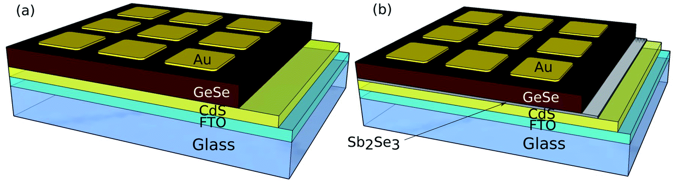 | ||
| Fig. 1 The two different device structures investigated: (a) FTO/CdS/GeSe/Au and (b) FTO/CdS/Sb2Se3/GeSe/Au. Each device structure was made with both Ag-doped and undoped GeSe versions, making four device configurations in total. | ||
Scanning electron microscopy (SEM) was performed with a JEOL 6610 microscope at 10 kV acceleration voltage.
XRD measurements were performed using a Panalytical X’Pert Pro instrument with a rotating cobalt anode, under ambient conditions. Monochromated incident radiation (Co Kα1) was used to perform θ![[thin space (1/6-em)]](https://www.rsc.org/images/entities/char_2009.gif) :2θ scans carried out between 25° and 95° in parallel beam geometry for both powder and film measurements.
:2θ scans carried out between 25° and 95° in parallel beam geometry for both powder and film measurements.
Current–voltage (J–V) measurements were performed to measure the power conversion efficiencies (PCEs) of all the devices. The measurements were completed under AM1.5 illumination provided by a TS space systems solar simulator calibrated by a photodiode. External quantum efficiency (EQE) measurements were completed using a Bentham PVE300 characterization system. Capacitance voltage (CV) measurements were carried out using a Boonton 7200 Capacitance Meter in ±500 mV range.
3 Results and discussion
3.1 Bulk crystals and powders
Powder XRD was performed on the undoped and Ag-doped materials, as shown in Fig. 2(a). The Bragg peak positions are taken from single crystal X-ray diffraction data of GeSe.1 The Ag-doped GeSe powder shows no additional peaks compared to the undoped GeSe, suggesting that no secondary phases have occurred. Table 1 shows the lattice parameters measured for both samples calculated using the data in Fig. 2(a), as shown in the ESI.† The lattice parameters for the undoped material agree with the single crystal X-ray diffraction data. For the Ag-doped material, all three lattice parameters increase, consistent with the larger size of silver atoms compared with that of germanium atoms and implying substitutional incorporation as AgGe.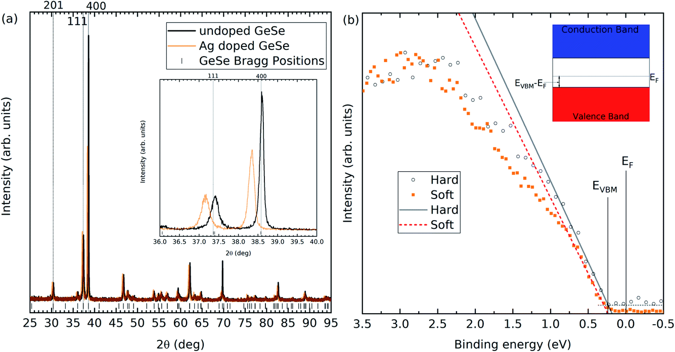 | ||
| Fig. 2 (a) Powder XRD for undoped and Ag-doped materials. Bragg peaks for the 201, 111, and 400 reflections are shown with dotted lines. The inset shows the same data zoomed into the 111 and 400 peaks to highlight the shift in pattern. (b) The valence band measurements for the Ag-doped GeSe for hard and soft X-ray photoemission. The inset is a diagram explaining how the Fermi level position can be calculated using the signal onset. | ||
| Lattice parameter | Undoped (Å) | Ag-doped (Å) |
|---|---|---|
| a | 10.828(9) | 10.866(9) |
| b | 3.834(5) | 3.844(5) |
| c | 4.382(6) | 4.433(6) |
ICP-OES was used to calculate the concentration of Ag atoms within the GeSe. Within the undoped GeSe, there are approximately 2.2 × 10²² atoms cm−3. The density of silver atoms present for the Ag doped GeSe is approximately 1.6 × 10¹⁸ atoms cm−3, which matches the target of 0.01 molar% Ag levels. No traces of Ag are found in the undoped GeSe.
Hard and soft X-ray photoemission spectroscopy was used to determine the Fermi level positions of the undoped and Ag-doped GeSe. In calibrated photoemission spectroscopy, 0 eV binding energy is equal to the Fermi level for the material. Therefore, measuring the valence band onset determines the separation between the valence band maximum and the Fermi level. In this scenario, a smaller difference would indicate a more p-type material. Soft X-ray photoemission spectroscopy is more surface sensitive than hard X-ray photoemission. The results from the undoped GeSe have been published previously2 and the Ag-doped valence band onsets are shown in Fig. 2(b), while all values are shown in Table 2.
| Photoemission | Undoped VBM − EF (eV) | Ag-doped VBM − EF (eV) |
|---|---|---|
| Hard | 0.30 ± 0.05 | 0.23 ± 0.05 |
| Soft | 0.33 ± 0.05 | 0.26 ± 0.05 |
GeSe has a band gap of 1.3 eV.1 Therefore, any valence band maximum less than 0.65 eV from the Fermi level suggests a p-type material. The undoped GeSe is p-type according to both the soft and hard X-ray photoemission spectroscopy, which is consistent with previous work that suggests the material is natively p-type.25,26 Furthermore, the results in both the soft and hard X-ray photoemission spectroscopy indicate that the Ag-doped GeSe has a higher hole density than the undoped GeSe. The VBM to Fermi level separations have been plotted in Fig. 3(a) for the two photon energies for the Ag-doped and undoped GeSe – the depths at which they are plotted correspond to three times the inelastic mean free path (IMFP) for the valence band photoelectrons for each photon energy. IMFP values were calculated using the TPP-2M method.29 Three times the IMFP corresponds to the depth from which 95% of the measured photoelectrons escape the material, according to the Beer–Lambert law. This data has been used to estimate the surface band bending and charge profiles by solving the Poisson equation.30 The hole effective masses and the dielectric constants used to solve the Poisson equation were taken from the literature and isotropically averaged by taking the cubed root of their product.31,32 The results are shown in Fig. 3. The bulk acceptor densities used as the bulk boundary condition for the Poisson solution are those determined from capacitance–voltage measurements on solar cell devices – see Section 3.3. The GeSe layers in the devices are made from the same GeSe source material as the crystals used for the photoemission measurements, so the doping level is expected to be similar. The resulting hole densities are 1.9 × 1016 cm−3 for the Ag-doped GeSe and 5.2 × 1015 cm−3 for the undoped GeSe. Downward band bending occurs at the surface, corresponding to a hole depletion layer. This is consistent with positively charged donor-type surface states with their charge being balanced by the negatively-charged background acceptors in the depletion region. The higher hole density for the Ag-doped material more effectively screens the surface states and hence leads to a narrower depletion region – the bulk carrier density is reached by ∼200 nm compared with ∼400 nm for the undoped GeSe (see Fig. 3).
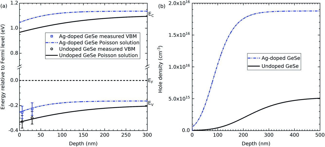 | ||
| Fig. 3 (a) The VBM positions relative to the Fermi level, EF, determined by photoemission spectroscopy for Ag-doped and undoped GeSe (points) and the band bending profiles obtained by solving the Poisson equation (lines); (b) the hole density versus depth corresponding to the band bending profiles shown in (a). | ||
3.2 Thin films
Thin films of both Ag-doped and undoped GeSe were deposited on both CdS and a 10 nm Sb2Se3 interfacial layer on CdS. The films were then annealed at temperatures determined by the optimised solar cell device results presented below. For both the Ag-doped and undoped films with no interfacial layer, the annealing conditions were 400 °C for 10 minutes, whereas for the Ag-doped and undoped films with the Sb2Se3 interfacial layer, the annealing conditions were 375 °C for 20 minutes.SEM images of all four structures after annealing are shown in Fig. 4. The undoped films (b) and (d) have lenticular grains at the GeSe surface 0.5–1 μm wide and 2–4 μm long. However, the silver doped films show different morphologies, with the film being grown with no interfacial layer (a) showing striking nodular features 0.5 nm in size and having bright contrast and that on the Sb2Se3 interfacial layer (c) having a less-distinct grain structure. We considered the origin of the bright contrast in (a): the ‘secondary electron’ detector used to record the images collects a majority of secondary electrons but also a minor fraction of primary electrons, which give compositionally sensitive contrast. Since the average atomic number of GeSe (31) is considerably lower than that of AgSe (40.5), it would be expected that AgSe would give bright contrast. However, this seems unlikely since the nominal composition of the films is just 0.01 atomic% Ag. The alternative explanation is that there is enhanced secondary electron emission from the nodules for morphological reasons. The nature of the nodules should therefore be examined in more detail with energy dispersive X-ray analysis and higher resolution imaging in the SEM.
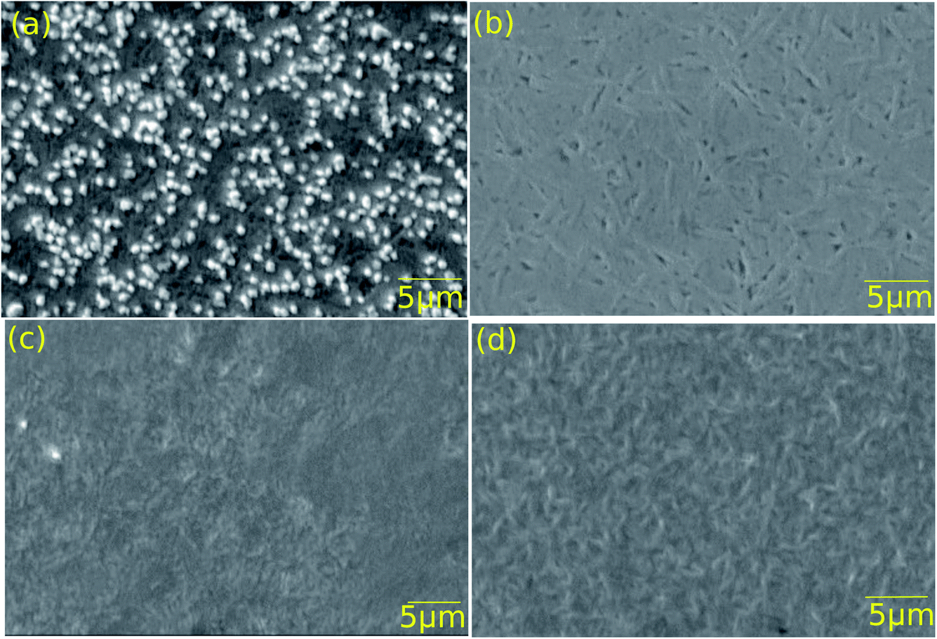 | ||
| Fig. 4 Scanning electron microscopy images for devices (a) FTO/CdS/Ag:GeSe, (b) FTO/CdS/u:GeSe, (c) FTO/CdS/Sb2Se3/Ag:GeSe, and (d) FTO/CdS/Sb2Se3/u:GeSe, where Ag is the silver doped samples and u is undoped samples. | ||
Thin film XRD has been performed on all four films and is shown in Fig. 5. Each of the peaks for all of the films is consistent with either GeSe or the SnO2:F coated substrate (see * on Fig. 5). The major difference that the incorporation of the Sb2Se3 interfacial layer appears to have on the structure of the undoped GeSe is the introduction of the Bragg peaks related to the 011, 111, and 311 reflections. The ratio of intensities of the 111 reflection to the 400 reflection suggests that the (111) plane is becoming more prominent relative to the (100) plane that the 400 reflection involves. Previous literature studying the structure of thin film GeSe has shown a strong orientation preference for the (100) plane experimentally and a theoretical study shows that the total energy of the plane is lower than those of alternative common planes.19–22,33,34 The incorporation of the Sb2Se3 interfacial layer has been shown previously to make the (111) plane more prominent, consistent with the findings in this study.23
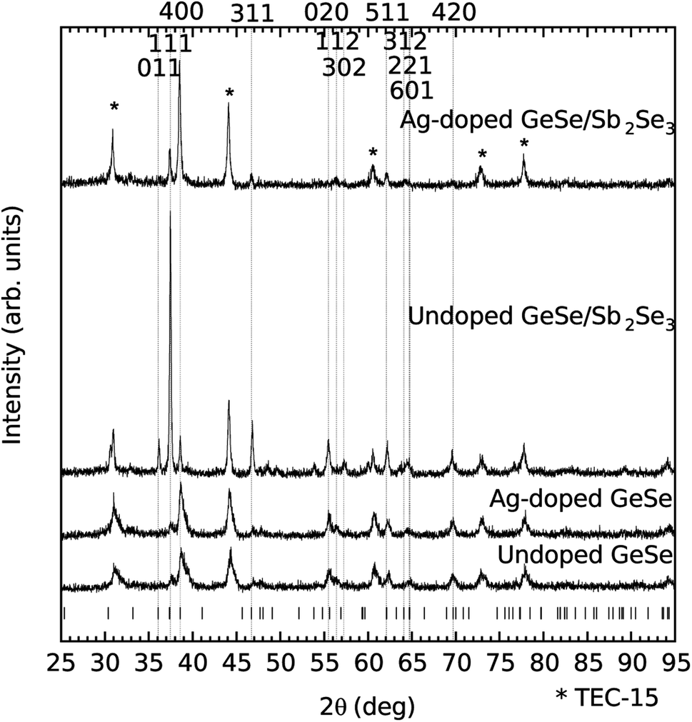 | ||
| Fig. 5 Thin film XRD of the four film stacks along with the GeSe Bragg peak positions.1 Relevant Bragg peak positions are labelled and positions related to the SnO2:F coated substrate are starred. | ||
3.3 Devices
All four device structures were processed into solar cells and the annealing temperatures optimised. CV measurements were performed on all four devices to determine the doping densities and are presented in the ESI.† For the Ag-doped GeSe with an Sb2Se3 interfacial layer, a doping density value could not be accurately determined due to a nonlinear line shape near to 0 V, an indication that the device has an interfacial barrier at the junction, which would explain its poor device performance. Therefore, to get a reliable comparison of the hole density with and without the Ag dopant, only the devices with no Sb2Se3 interfacial layer were used. The Ag-doped GeSe sample has an acceptor density of 1.9 × 1016 cm−3 compared to the undoped GeSe sample with an acceptor density of 5.2 × 1015 cm−3. The undoped GeSe with an Sb2Se3 interfacial layer showed a similar acceptor density of 4.6 × 1015 cm−3, comparable to that of the undoped GeSe cell with no interfacial layer. This suggests that the incorporation of the Ag into the films is increasing the acceptor density by a factor of ∼3.5. Therefore, assuming no other effects, Ag-doping should ultimately be beneficial for PV performance. The CV-determined acceptor density is approximately two orders of magnitude lower than the silver atomic density estimated from ICP-OES for the Ag-doped GeSe source material.Fig. 6 shows the J–V curves for the best contact for each of the optimised devices with the associated solar cell performance. Table 3 shows the average device parameters of all working contacts for the devices.
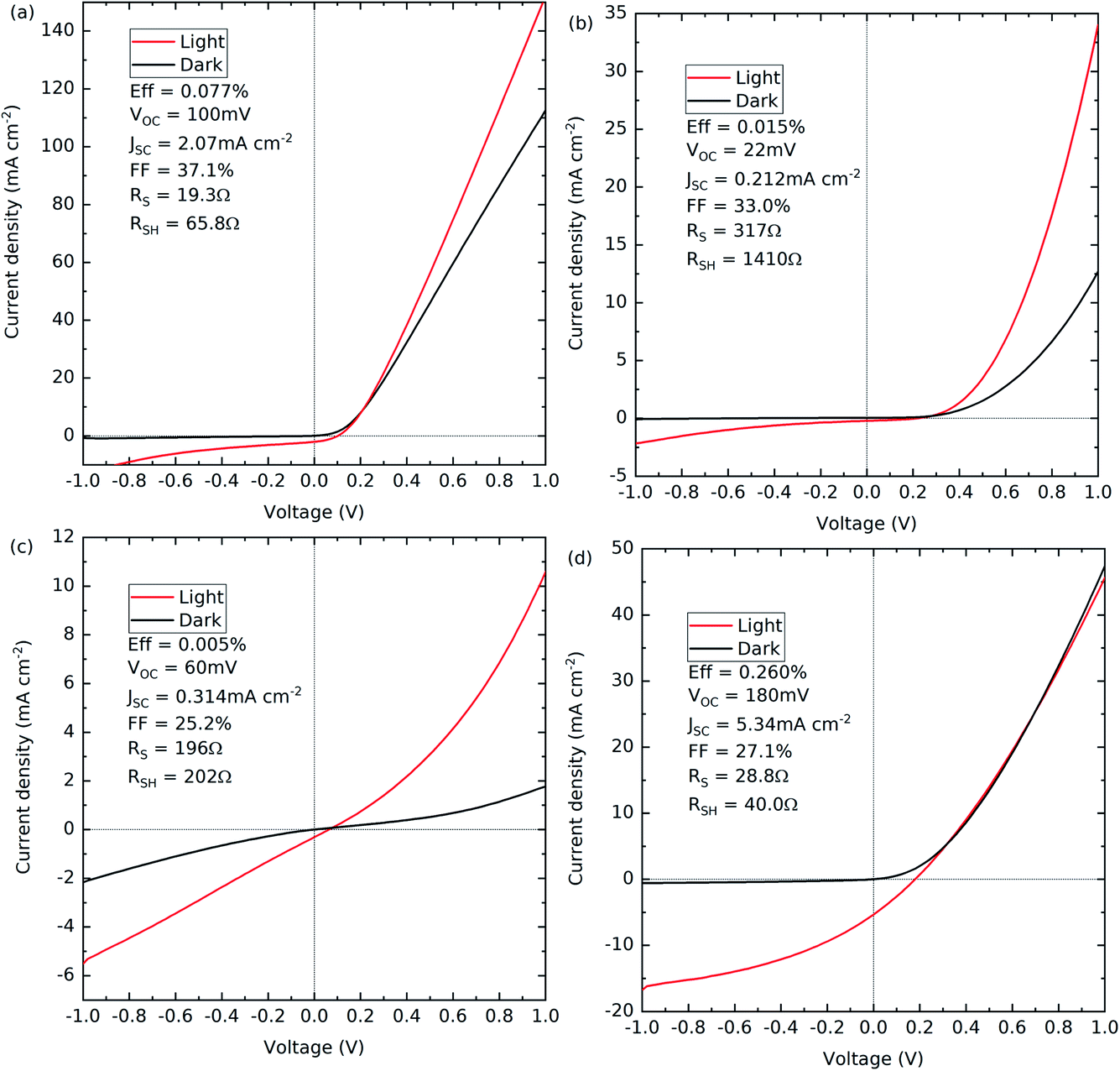 | ||
| Fig. 6 Current density vs. voltage measurements in the light and dark for devices (a) FTO/CdS/Ag:GeSe/Au, (b) FTO/CdS/u:GeSe/Au, (c) FTO/CdS/Sb2Se3/Ag:GeSe/Au, and (d) FTO/CdS/Sb2Se3/u:GeSe/Au, where Ag is the silver doped samples and u is undoped samples. | ||
| Device | Efficiency (%) | V OC mV | J SC mA cm−2 | FF% |
|---|---|---|---|---|
| FTO/CdS/Ag:GeSe/Au | 0.06 ± 0.02 | 90 ± 20 | 1.9 ± 0.2 | 32 ± 5 |
| FTO/CdS/u:GeSe/Au | 0.007 ± 0.005 | 120 ± 60 | 0.4 ± 0.3 | 27 ± 4 |
| FTO/CdS/Sb2Se3/Ag:GeSe/Au | 0.003 ± 0.001 | 50 ± 10 | 0.25 ± 0.04 | 24 ± 2 |
| FTO/CdS/Sb2Se3/u:GeSe/Au | 0.116 ± 0.06 | 170 ± 20 | 3.5 ± 1.2 | 26.8 ± 1.4 |
Fig. 6(a) and (b) show the J–V curves for the devices with no interfacial layer that have either Ag-doped or undoped GeSe, respectively. Both cells show a good diode shape in the dark but the overall cell performance is compromised by the low current. Furthermore, both have low VOC and limited fill factors due to high series and low shunt resistance. EQE measurements were performed on both samples (see the ESI†) to diagnose the cause of the low currents. No signal could be measured for the Ag-doped GeSe but for the undoped GeSe, the EQE shows a peak near to the CdS band gap energy (around 525 nm). This suggests a very narrow collection region, with potential causes being the low carrier lifetime, a narrow depletion region, or a thin material and thus low optical absorption. Given the acceptor densities reported here and the optical properties of GeSe, the second and third are unlikely.1
Fig. 6(c) and (d) show the devices with an Sb2Se3 interfacial layer that have either Ag-doped or undoped GeSe, respectively. The Ag-doped device with the Sb2Se3 interfacial layer is an extreme S-shape in the dark J–V compared with the other devices, suggesting a fundamental issue with the device. The origin of this is uncertain, but it could be due to interdiffusion of the films or the formation of an unwanted electrical barrier.
Fig. 6(d) shows the undoped device with the Sb2Se3 interfacial layer. The diode shape is broadly similar in the light and in the dark, but significantly higher current and voltage are produced under illumination, producing a power conversion efficiency of 0.260%. This may be due to an improvement in the built-in field of the interface but the fill factor is again low due to high series and low shunt resistance. There is no S-shape feature in the forward bias, suggesting that the issues do not stem from an interfacial barrier and performance may instead be limited by the absorber material itself. The EQE results support this conclusion, again showing a peak near to the CdS band gap energy. As discussed above, this is likely linked to the low carrier lifetime.
The inclusion of the Sb2Se3 interfacial layer improves the device performance for the undoped GeSe, rising from 0.015% efficiency to 0.260% efficiency. This is consistent with the previous record efficiency device result by Liu et al. for GeSe, which had a rise from 1.4% to 5.2% with the inclusion of the Sb2Se3 interfacial layer.23 What is also consistent with their findings is that the inclusion of the Sb2Se3 interfacial layer gives greater prominence to the (111) orientation relative to the (100) orientation in the XRD. Furthermore, the solar cells presented by Chen et al. that achieved a maximum efficiency of 0.27% are strongly (100) orientated with no indication of (111) orientation. Xue et al. achieved 1.48% efficiency with prominent (111) as well as (100) orientation. In combination, the literature appears to indicate that having the (111) orientation present is beneficial for improved device performance.
Conduction in the nanoribbon structure Sb2Se3 is known to be anisotropic, with the highest conductivity being along the covalently bonded ribbons.11,12 Similarly, since GeSe is a 2D material, it might be expected that if the sheets were perpendicular to the substrate in a PV device, there would be some benefit to performance. However, in the (100) orientation, the sheets are parallel to the substrate, which the Sb2Se3 literature would suggest is the least preferred to improve conductivity. This could explain why the cell performance, particularly the current, improves with the incorporation of the (111) orientation due to the improved conductivity along the sheets.
4 Conclusions
Ag-doped GeSe bulk crystals have successfully been synthesised by a melt growth method with no secondary phases resulting from the Ag incorporation. The CV, photoemission results and associated Poisson equation modelling show that the incorporated Ag led to the carrier concentration increasing from 5.2 × 1015 cm−3 to 1.9 × 1016 cm−3. However, this is significantly lower than the Ag-content in the source materials of 1.6 × 10¹⁸ atoms cm−3, estimated from ICP-OES. Undoped and Ag-doped GeSe films were deposited onto both FTO/CdS and FTO/CdS/Sb2Se3, which were later processed into solar cells. The Ag-doped and undoped GeSe films with no Sb2Se3 interfacial layer exhibit similar XRD patterns with the (100) orientation dominating. The inclusion of the Sb2Se3 interfacial layer leads to the (111) orientation being more prominent. The two cell structures with no interfacial layer show a reasonable diode shape in the dark but low overall cell performance in the light due to the low current. The proposed causes are linked to either a narrow depletion region and/or a low carrier lifetime. The cell structure with Ag-doped GeSe with an Sb2Se3 interfacial layer did not work in the light or dark, with CV measurements suggesting a barrier at the interface. The cell structure with undoped GeSe and an Sb2Se3 interfacial layer shows the best device performance with an efficiency of 0.260%. This improvement in efficiency with the Sb2Se3 interfacial layer is consistent with the increased proportion of the (111) orientation, as also found in a previous study.23 Despite the low device performance for the Ag-doped samples, the feasibility of Ag doping has been demonstrated and improved hole concentration should lead to improved device performance if the low carrier lifetime and the interface barrier for the devices can be resolved.Author contributions
Concept, project administration, investigation (XRD, J–V, EQE), formal analysis of all data by MJS. Writing (first draft) by MJS, supported by TDV. TPS and LT provided resources in terms of deposition of the CdS and Sb2Se3 films and TDCH supported the preparation of the samples for ICP-OES. MJS provided resources in terms of the GeSe source material, GeSe thin films and device processing. TB supported the powder and thin film XRD investigation. Photoemission instrumentation resources developed and maintained by PKT and TLL. JDM performed the CV investigation and supported MJS with the CV, J–V and EQE analysis. Photoemission investigation by LAHJ, MJS, LT, TDCH, LJP, CD supported by TDV, KD, PKT and TLL. The Poisson equation solving software written and used by TDV. Funding acquisition by KD. Writing (review and editing) by all authors. Supervision by JDM and TDV.Conflicts of interest
There are no conflicts to declare.Acknowledgements
Funding is acknowledged from the Engineering and Physical Sciences Research Council from the Centre for Doctoral Training in New and Sustainable PV (EP/L01551X/2), Doctoral Training Partnerships (EP/T517975/1, EP/R513271/1), fellowship and research grants (EP/N014057/1, EP/T006188/1), and a strategic equipment grant (EP/P001513/1). We acknowledge the Diamond Light Source for time on Beamline I09 under Proposal SI31170-1.Notes and references
- P. A. E. Murgatroyd, M. J. Smiles, C. N. Savory, T. P. Shalvey, J. E. N. Swallow, N. Fleck, C. M. Robertson, F. Jäckel, J. Alaria, J. D. Major, D. O. Scanlon and T. D. Veal, Chem. Mater., 2020, 32, 3245–3253 CrossRef CAS PubMed.
- M. J. Smiles, J. M. Skelton, H. Shiel, L. A. H. Jones, J. E. N. Swallow, H. J. Edwards, P. A. E. Murgatroyd, T. J. Featherstone, P. K. Thakur, T.-L. Lee, V. R. Dhanak and T. D. Veal, J. Mater. Chem. A, 2021, 9, 22440–22452 RSC.
- A. Tołłoczko, S. J. Zelewski, M. Błaszczak, T. Woźniak, A. Siudzińska, A. Bachmatiuk, P. Scharoch and R. Kudrawiec, J. Mater. Chem. C, 2021, 9, 14838–14847 RSC.
- W. Shockley and H. J. Queisser, J. Appl. Phys., 1961, 32, 510–519 CrossRef CAS.
- M. A. Green, E. D. Dunlop, J. Hohl-Ebinger, M. Yoshita, N. Kopidakis and X. Hao, Progr. Photovolt.: Res. Appl., 2020, 28, 629–638 CrossRef.
- A. M. Ganose, C. N. Savory and D. O. Scanlon, Chem. Commun., 2017, 53, 20–44 RSC.
- D. H. Fabini, R. Seshadri and M. G. Kanatzidis, MRS Bull., 2020, 45, 467–477 CrossRef.
- R. E. Brandt, V. Stevanović, D. S. Ginley and T. Buonassisi, MRS Commun., 2015, 5, 265–275 CrossRef CAS.
- Z. Li, X. Liang, G. Li, H. Liu, H. Zhang, J. Guo, J. Chen, K. Shen, X. San, W. Yu, R. E. I. Schropp and Y. Mai, Nat. Commun., 2019, 10(125), 1–9 Search PubMed.
- C. H. Don, H. Shiel, T. D. C. Hobson, C. N. Savory, J. E. N. Swallow, M. J. Smiles, L. A. H. Jones, T. Featherstone, P. K. Thakur, T. L. Lee, K. Durose, J. D. Major, V. Dhanak, D. O. Scanlon and T. D. Veal, J. Mater. Chem. C, 2020, 8, 12615–12622 RSC.
- Y. Zhou, L. Wang, S. Chen, S. Qin, X. Liu, J. Chen, D.-J. Xue, M. Luo, Y. Cao, Y. Cheng, E. H. Sargent and J. Tang, Nat. Photonics, 2015, 9, 409–415 CrossRef CAS.
- L. Wang, D. B. Li, K. Li, C. Chen, H. X. Deng, L. Gao, Y. Zhao, F. Jiang, L. Li, F. Huang, Y. He, H. Song, G. Niu and J. Tang, Nat. Energy, 2017, 2, 17046 CrossRef CAS.
- S.-C. Liu, Y. Yang, Z. Li, D.-J. Xue and J.-S. Hu, Mater. Chem. Front., 2020, 4, 775–787 RSC.
- G. Shi and E. Kioupakis, Nano Lett., 2015, 15, 6926–6931 CrossRef PubMed.
- C. Xia, J. Du, W. Xiong, Y. Jia, Z. Wei and J. Li, J. Mater. Chem. A, 2017, 5, 13400–13410 RSC.
- X. Lv, W. Wei, C. Mu, B. Huang and Y. Dai, J. Mater. Chem. A, 2018, 6, 5032–5039 RSC.
- Y. Mao, C. Xu, J. Yuan and H. Zhao, J. Mater. Chem. A, 2019, 7, 11265–11271 RSC.
- G.-J. Hou, D.-L. Wang, R. Ali, Y.-R. Zhou, Z.-G. Zhu and G. Su, Sol. Energy, 2018, 159, 142–148 CrossRef.
- D.-J. Xue, S.-C. Liu, C.-M. Dai, S. Chen, C. He, L. Zhao, J.-S. Hu and L.-J. Wan, J. Am. Chem. Soc., 2017, 139, 958–965 CrossRef CAS PubMed.
- S.-C. Liu, Y. Mi, D.-J. Xue, Y.-X. Chen, C. He, X. Liu, J.-S. Hu and L.-J. Wan, Adv. Electron. Mater., 2017, 3, 1700141 CrossRef.
- B. Chen, G. Chen, W. Wang, H. Cai, L. Yao, S. Chen and Z. Huang, Sol. Energy, 2018, 176, 98–103 CrossRef CAS.
- B. Chen, Y. Ruan, J. Li, W. Wang, X. Liu, H. Cai, L. Yao, J.-M. Zhang, S. Chen and G. Chen, Nanoscale, 2019, 11, 3968–3978 RSC.
- S.-C. Liu, C.-M. Dai, Y. Min, Y. Hou, A. H. Proppe, Y. Zhou, C. Chen, S. Chen, J. Tang and D.-J. Xue, et al. , Nat. Commun., 2021, 12, 670 CrossRef CAS PubMed.
- T. D. C. Hobson, L. J. Phillips, O. S. Hutter, H. Shiel, J. E. N. Swallow, C. N. Savory, P. K. Nayak, S. Mariotti, B. Das, L. Bowen, L. A. H. Jones, T. J. Featherstone, M. J. Smiles, M. A. Farnworth, G. Zoppi, P. K. Thakur, T.-L. Lee, H. J. Snaith, C. Leighton, D. O. Scanlon, V. R. Dhanak, K. Durose, T. D. Veal and J. D. Major, Chem. Mater., 2020, 32, 2621–2630 CrossRef CAS.
- D. S. Kyriakos and A. N. Anagnosopoulos, J. Appl. Phys., 1985, 58, 3917–3920 CrossRef CAS.
- D. D. Vaughn, R. J. Patel, M. A. Hickner and R. E. Schaak, J. Am. Chem. Soc., 2010, 132, 15170–15172 CrossRef CAS PubMed.
- N. S. Avasarala, B. Govoreanu, K. Opsomer, W. Devulder, S. Clima, C. Detavernier, M. van der Veen, J. Van Houdt, M. Henys, L. Goux and G. S. Kar, 2017 47th European Solid-State Device Research Conference (ESSDERC), 2017, pp. 168–171 Search PubMed.
- Z. Shu and Y. Cai, J. Mater. Chem. C, 2020, 8, 13655–13667 RSC.
- S. Tanuma, C. Powell and D. Penn, Surf. Interface Anal., 2003, 35, 268–275 CrossRef CAS.
- T. D. Veal, L. F. J. Piper, M. R. Phillips, M. H. Zareie, H. Lu, W. J. Schaff and C. F. McConville, Phys. Status Solidi A, 2006, 203, 85–92 CrossRef CAS.
- H. Chandrasekhar and U. Zwick, Solid State Commun., 1976, 18, 1509–1513 CrossRef CAS.
- Q. Fan, J. Yang, J. Cao and C. Liu, R. Soc. Open Sci., 2021, 8, 6 Search PubMed.
- W. Zi, F. Mu, X. Lu, Y. Cao, Y. Xie, L. Fang, N. Cheng, Z. Zhao and Z. Xiao, Sol. Energy, 2020, 199, 837–843 CrossRef CAS.
- S.-C. Liu, Y. Yang, X. Zhang, L.-B. Huang, J.-K. Sun, B. Guan, X. Li, D.-J. Xue and J.-S. Hu, Phys. Status Solidi RRL, 2018, 12, 1800370 CrossRef.
Footnote |
| † Electronic supplementary information (ESI) available. See https://doi.org/10.1039/d2fd00048b |
| This journal is © The Royal Society of Chemistry 2022 |