 Open Access Article
 This Open Access Article is licensed under a
 Creative Commons Attribution 3.0 Unported Licence
Ultrathin wide band gap kesterites†
Charlotte
Platzer Björkman
 *,
Jes K.
Larsen
,
Nishant
Saini
,
Melike
Babucci
and
Natalia
Martin
*,
Jes K.
Larsen
,
Nishant
Saini
,
Melike
Babucci
and
Natalia
Martin
Div. Solar Cell Technology, Dep. Materials Science and Engineering, Uppsala University, Sweden. E-mail: charlotte.platzer@angstrom.uu.se
First published on 13th April 2022
Abstract
Kesterite Cu2ZnSnS4 (CZTS), used for thin film solar cells, has a band gap energy around 1.5–1.6 eV with possibilities for further increase through alloying. In some applications for wide band gap solar cells, reduced absorber thickness can be beneficial, to allow partial light transmission. Reduced thickness can also be beneficial to reduce bulk recombination, and so called ultrathin solar cells (<700 nm thick) have been studied for several materials systems. Here, we report performance for CZTS devices down to 250 nm thickness and show that performance loss from thickness reduction is relatively small, partly due to short minority carrier diffusion length. Insertion of thin passivation layers (Al2O3, SiO2 or HfO2) at the Mo/CZTS interface gives improved performance of ultrathin devices, from 4.7% to 5.6% efficiency for best performing cells having 250 nm thick CZTS with Mo as compared to Mo/Al2O3 back contact. The approach of NaF post deposition for making isolating passivation layers conductive is tested for the first time for CZTS and is shown to work. For fabrication of CZTS devices on transparent ITO back contact, the insertion of passivation layers can reduce diffusion of indium into CZTS, but device performance is lower than on Mo back contacts.
Introduction
There is large interest in finding stable, environmentally friendly, and cost-efficient wide band gap materials that could be used in applications such as semi-transparent modules, water splitting or as top cell materials for tandem solar cells. Perovskite/Si and perovskite/Cu(In,Ga)Se2 (CIGS) tandems have reached high efficiencies (24–29.5%)1 and some commercial efforts are ongoing. Other options for tandem top cells are III–V materials where high efficiency of up to 32.8% has been shown,1 but where the possibility to reduce production cost has been questioned.2 The possibility of tuning the band gap of CIGS or kesterites to larger energies than those used in record single junction devices has also been investigated.3–5 In this work we study kesterite Cu2ZnSnS4 (CZTS) devices with band gap energy of 1.5–1.6 eV, with significantly reduced thickness, which could be suitable for use as the top cell in a tandem structure if efficiency can also be increased.6,7 By thinning down the absorber, current matching in a 2-terminal tandem structure can be achieved. A thin absorber can also be beneficial to reduce bulk recombination, but at the same time back contact passivation becomes more important.8 For some applications the absorption loss from thinning down the absorber is not important, or even wanted. For other applications absorption losses should be minimized, and then advanced measures for back contact reflection and light trapping are needed.In our previous work, we investigated the influence on device performance of variation of the CZTS thickness in a standard Mo/CZTS/CdS/ZnO/ZnO:Al device structure.9 The thickness was varied from 2000 nm down to 500 nm, and significant drop in performance was seen in all solar cell parameters for thicknesses below 750 nm. By comparing external quantum efficiency (EQE) at short circuit conditions and under −0.5 V reverse bias, we concluded that there was no gain in collection of minority carriers for increased thickness above 750–1000 nm. In later work, by us and others,10 relatively good performance has been seen for even lower CZTS thicknesses, of around 300 nm. In this work we therefore revisit thickness variation in CZTS, and include studies of back contact passivation and transparent back contacts. For CZTS, back contact dielectric passivation layers have been studied not only for potential reduction of back contact recombination,11 but also for engineering of back contact reactions during annealing.12–14 Since carrier transport across the passivation layer is needed for the solar cell to work, the layers must either be ultrathin, conductive or with openings in thicker layers.
A few studies have highlighted that NaF can be used to create openings in rear-contact dielectric passivation layers without the need of patterning. This was first demonstrated by Ledinek et al. in 2018 for CIGS deposited on Al2O3 passivation layers.15 They found that the current was blocked in devices with 6 nm Al2O3 passivation layers, but if a NaF precursor was evaporated onto the passivation layer prior to CIGS deposition, the current was not blocked. TEM studies of the devices indicated that the presence of NaF resulted in formation of contact openings in the passivation layer.15 Birant et al. demonstrated that spin coating of a NaF solution onto a Al2O3 passivation layer prior to selenization at 540 °C resulted in formation of openings in the Al2O3 layer.16 This was subsequently used to produce CIGS devices with increased open circuit voltage (VOC), which was ascribed to back contact passivation.16 The same authors likewise demonstrated the same approach to create openings in 2 nm thick HfO2.17 The studies demonstrating creation of contact openings in dielectric passivation layers so far use selenium containing CIGS absorbers. It is not yet clear if selenium plays a key role in creation of contact openings. Here it is investigated if this approach can likewise be applied in CZTS, which contains sulfur instead of selenium.
Finally, the performance of optimized thin CZTS devices is compared to our baseline devices with standard thickness and with CIGS devices with varying thickness and band gap energy. We discuss possible routes for improved performance of thin CZTS devices in combination with band gap increase.
Experimental
CZTS absorbers were produced with a two-step approach relying on deposition of precursors by sputtering followed by annealing in sulfur-containing atmosphere. Most devices were deposited on Mo coated soda-lime glass and some on Indium Tin Oxide (ITO) The about 300 nm thick Mo back contact layer was prepared by DC-sputtering and the ITO was deposited using sputtering of ITO target in the presence of a mixture of Ar and O2. A thickness of around 250 nm was deposited and sheet resistivity of the layers was approximately 35 Ω □−1.Passivation layers of Al2O3 and SiO2 were sputter deposited on Mo and ITO-coated glass. The thickness of the coatings were estimated from the deposition rate of thicker layers. Al2O3 was sputter-deposited using a metallic Al target in the presence of 100 sccm Ar and 40 sccm O2. SiO2 was sputter deposited using a Si target in the presence of 40 sccm Ar and 20 sccm O2.
Al2O3 or HfO2 dielectric layers were grown on the Mo (or ITO for Al2O3) layer by atomic layer deposition (ALD) in a Picosun R200 system. The Al2O3 layer was grown with trimethylaluminum (TMA) and H2O. For a series comparing sputtered and ALD Al2O3 on Mo and ITO, a substrate temperature of 200 °C was used and the number of deposition cycles varied from 10 to 100, while for the series exploring NaF post treatments a substrate temperature of 100 °C and 62 cycles was used. The HfO2 layer was grown with 45 cycles tetrakis(dimethylamino)hafnium (TDMAH) and H2O at a substrate temperature of 170 °C. The thicknesses of the dielectric layers were determined by ellipsometry to be 5.5 nm and 5.6 nm for Al2O3 and HfO2 respectively. For some samples a 5 nm NaF layer was evaporated onto the passivation layer prior to CZTS precursor deposition. For another set of samples the NaF layer was instead deposited onto the CZTS precursor surface before sulfurization. References without NaF addition were also included.
CZTS precursors were sputtered from CuS, SnS, and ZnS binary targets with substrate temperature of 250 °C. The composition of the precursors was measured by X-ray fluorescence. Precursors with composition ratios Cu/Sn = 1.85 and Zn/(Cu + Sn) = 0.34 were used. All samples in the series were deposited in the same sputtering run and annealed together. For another set of samples with various CZTS absorber thicknesses (350 nm, 500 nm, 750 nm, 1000 nm), samples were deposited directly on the Mo-coated soda lime glass. The compositions of these precursors are given in Table S1 in the ESI.†
Sulfurization of the precursors was performed in a pyrolytic carbon coated graphite box containing 160 mg of sulfur. The graphite box was introduced into a preheated tube furnace with an argon background pressure of 350 torr. When samples were transferred to the hot zone, the temperature of the box rose to 565 °C in about 90 s. The samples were then allowed to dwell for 13 min before they were moved to the cold zone and allowed to cool to room temperature. For a more detailed description of the annealing process, see ref. 18.
Samples went through a two-step air annealing treatment (80 s at 300 °C and 600 s at 200 °C) after sulfurization as described in ref. 19. Before buffer layer deposition, the absorbers were etched for 2 min in 5% KCN. An about 60 nm thick CdS layer was deposited by chemical bath deposition at 60 °C following the procedure described in ref. 20. The devices were completed by sputter deposition of an i-ZnO/Al:ZnO bilayer and mechanical scribing to define cells with an area of 0.05 cm2. Dark and illuminated J–V measurements and quantum efficiency measurements were performed with homebuilt setups. Scanning electron microscopy (SEM) was performed in a Zeiss LEO 1550 instrument with an in-lens detector and an acceleration voltage of 5 or 20 kV. Glow discharge optical emission spectroscopy (GDOES), was performed in a Spectruma Analytik GDS750HR analyser with Ar as the sputtering gas and a 2 mm probing diameter.
Results and discussion
Thickness variation in CZTS revisited
In Fig. 1, VOC values from our previously published thickness series9 are shown together with new data. (All device parameters are given in Table S1.†) The published data cover absorber thicknesses from 2000 nm down to 500 nm, while the new experiments are for 1000 nm down to 300 nm CZTS thickness. The trend is the same in these two series, i.e. decreasing VOC and short circuit current density (JSC) with decreasing absorber thickness, but the absolute values differ. The loss in performance below 750 nm is much stronger in previous work, and also, the gain in thickness increase is limited in the new series. The champion device for 300 nm thickness from repeated experiments is also given and in Table S1† also a more recent champion device for intermediate (1200 nm) thickness.21 The efficiency and solar cell parameters for the thinnest device are close to that achieved for the thickest devices in the previous thickness series.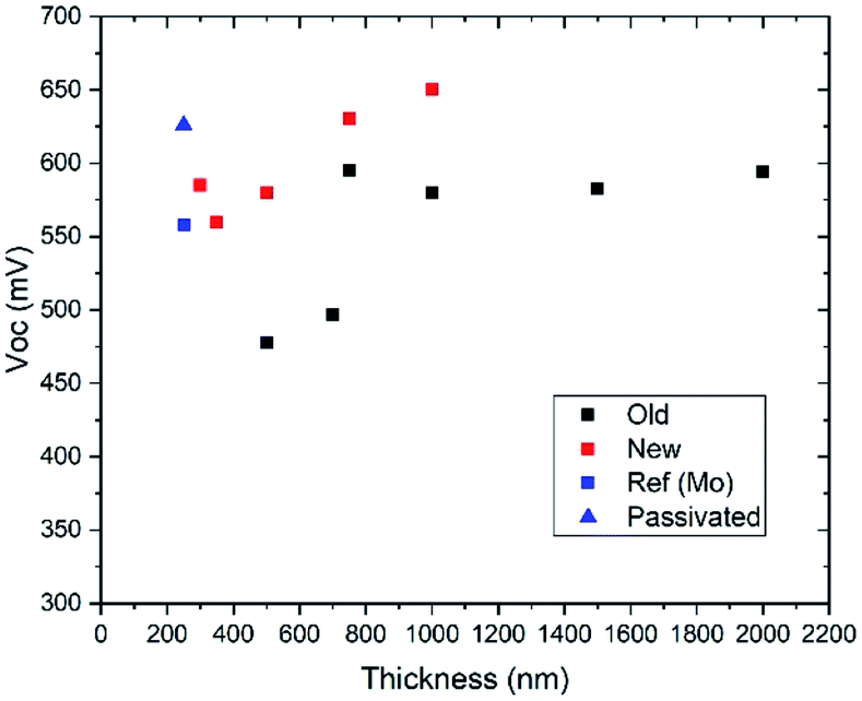 | ||
| Fig. 1 V OC as a function of absorber thickness comparing published data (black) and new data (red), all on Mo back contact. Two devices (blue) from a different series using 250 nm thick CZTS comparing Mo and Mo/Al2O3 back contact are also shown (see Table 2). | ||
In connection to the previously published thickness series, device modelling in SCAPS was performed.22 A model for the thick, reference device was established based on optical data from ellipsometry23 and device characterisation.24 The experimental results from the thickness series were partly reproduced in modelling, but the drastic drop in performance for thinnest absorbers was not seen. It was concluded that additional losses, likely due to strong influence from segregated secondary phases, were present in the thinnest devices. The smaller performance drop for the thinnest devices in the new device series, could possibly be connected to a precursor composition closer to stoichiometry that should result in reduced segregation of secondary phases.
Optimisation of absorber annealing should allow recrystallisation into large grains, control secondary phase segregation and provide sufficient S and SnS partial pressure. As we showed in ref. 21, these can be competing processes. In a comparison of annealing of 1200 nm thick CZTS precursors for 1 and 13 minutes, we showed large grains, extending through the complete absorber thickness, after 13 min, but this together with segregation of SnS2 at the back contact. The FF and device performance were suppressed by a current blocking behaviour that we tentatively attributed to the extensive SnS2 back contact layer. For the 1 min anneal, smaller grains were obtained and a more dispersed secondary phase segregation. The 1 min device showed reduced JSC and EQE level but no current blocking behaviour.
For a thinner absorber, the time for recrystallisation to achieve grains extending the complete absorber depth should be shorter than for much thicker layers. For annealing conditions where loss of S and SnS partial pressure occurs over time, this means that process optimisation in terms of for example SnS supply can be expected to be different for different absorber thicknesses.
In the SCAPS reference model referred to above,22 significant interface recombination (IR) was included, since this has been concluded for CZTS/CdS junctions.24 In the same work this model was also compared to a model where IR was negligible but all other parameters kept constant. Batch calculations for different minority carrier diffusion length and varying absorber thickness were performed. In that case, the performance drop for thinner absorbers was dominated by back contact recombination. In order to investigate if this is really the case, and if performance of very thin CZTS can be improved by back contact passivation, such experiments were conducted.
Back contact passivation using Al2O3 and SiO2 as passivation layer
A set of experiments were performed using 300 nm thick CZTS and thin Al2O3 or SiO2 back contact passivation layers below the CZTS. Both Mo and transparent ITO back contacts were used and passivation layers were deposited by either sputtering (SiO2 and Al2O3) or atomic layer deposition (Al2O3). The thickness of the passivation layer was varied from around 1 nm to 10 nm. The thickest passivation layers caused severe delamination.A comparison of device performance with and without 1 nm Al2O3 for Mo and ITO reference devices is shown in Table 1. The devices on ITO are both poor, but the device with Al2O3 back contact layer has lower performance due to an s-shaped I–V curve and reduced FF. SEM cross sections of the reference devices are shown in Fig. 2. The crystallinity of the CZTS on ITO is worse with smaller grains as compared to that on Mo.
| Sample | V OC [mV] | J SC [mA cm−2] | FF [%] | Eff. [%] |
|---|---|---|---|---|
| ITO ref. (B686) | 398 | 10.7 | 53.2 | 2.3 |
| ITO/ALD Al2O3 1 nm | 331 | 11.1 | 36 | 1.3 |
| Mo ref. (B681) | 585 | 16.1 | 59 | 5.6 |
| Mo/ALD Al2O3 1 nm | 598 | 16.5 | 62.2 | 6.2 |
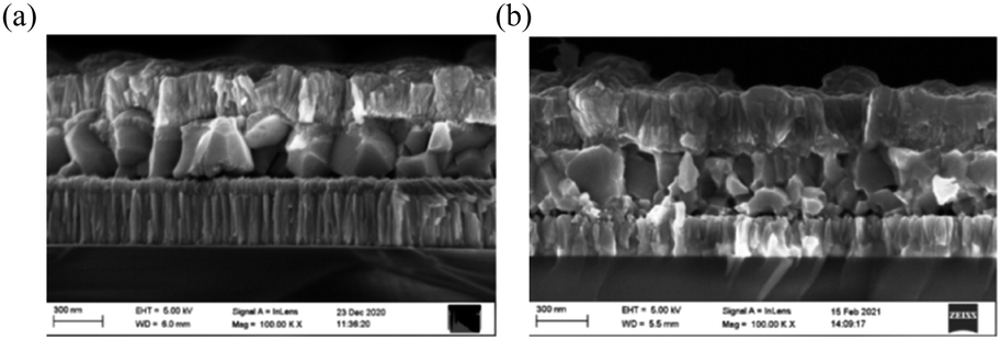 | ||
| Fig. 2 CZTS device on (a) Mo and (b) ITO. Device data are given in Table 1 (reference devices). | ||
For CZTS on ITO without passivation layer, depth profiling using GDOES showed indium diffusion into the CZTS (Fig. S2 and S3, ESI†). Such reactions between CZTS and TCOs after absorber annealing has been shown before.25,26 When the passivation layers are inserted, the indium signal in CZTS decreased with increasing Al2O3 or SiO2 thickness indicating that the passivation layer can limit this reaction. The reason for poor recrystallisation of CZTS on the ITO back contacts could maybe be related to limited Na supply. However, Na, diffusing from the glass, was detected in the CZTS at similar levels regardless of passivation layer thickness. The Na signal was also similar for Mo and ITO back contacts.
For devices on Mo, the insertion of an ultrathin passivation layer resulted in slightly improved performance for ALD Al2O3 and sputtered SiO2 (Fig. 3). Devices with increasing passivation layer thickness showed increasing blocking behaviour as can be expected for sufficiently thick insulating layers. Such improvements in device performance by introduction of ultrathin Al2O3 layers between Mo and CZTS has been shown by other groups.8 In their case, a non-conformal coverage of the oxide after annealing of a 400 nm thick CZTS was seen in high resolution TEM. The insertion of the oxide improved device performance, and improved morphology with fewer voids and ZnS segregation was seen. It is not clear if such an ultrathin oxide can provide significant electrical passivation, or if the main benefit is control of the chemical interface during annealing. In order to apply thicker passivation layers, approaches for conduction control through the layers are needed such as patterning or, as explored in this work, the application of NaF.
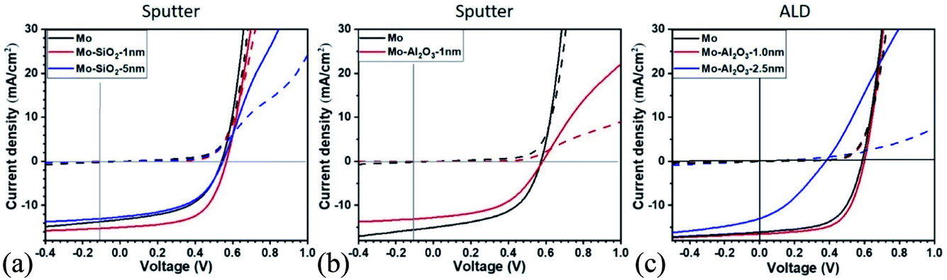 | ||
| Fig. 3 I–V curves for devices with back contact passivation layers (a) SiO2 by sputtering, (b) Al2O3 by sputtering and (c) Al2O3 by ALD, compared to Mo reference devices. | ||
Effect of NaF on charge transport properties of HfO2 and Al2O3 passivation layers
A set of devices with 250 nm thick CZTS were produced to evaluate the potential of NaF to allow charge transport through 5 nm thick HfO2 and Al2O3 passivation layers. It was investigated if NaF must be deposited directly onto the passivation layer in order to have the desired effect, or if it is preferable to deposit the NaF on top of the CZTS precursor prior to annealing.Fig. 4 shows the J–V curves of the best device in the set of samples. The samples in Fig. 4(a) were produced without addition of NaF. These are references meant to evaluate if the passivation layer results in current blocking if NaF is not introduced. The J–V curve of the device without passivation layer (Mo in Fig. 4(a)) shows that the current is not blocked as expected in absence of passivation layer. The sample with HfO2 passivation layer is, however, much poorer due to a kink in the J–V curve and a low slope of both dark and light curves, which indicates that the current is blocked in these samples. Unfortunately the samples of Al2O3 completely delaminated, and could not be evaluated. Based on the reference and HfO2 devices, it appears that introduction of a 5 nm thick passivation layer causes blocking of the current in agreement with previous observations (see e.g. ref. 15) and the results presented in the previous section.
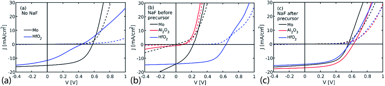 | ||
| Fig. 4 J–V curves of devices with either HfO2 or Al2O3 passivation layer and references without a dielectric interlayer (Mo). The solid lines are measured under illumination, while the dashed lines are measured in the dark. (a) No NaF was deposited on these samples. The Al2O3 sample completely delaminated and is therefore excluded. (b) NaF deposited onto the passivation layer before the CZTS precursor. (c) NaF deposited onto the CZTS precursor prior to annealing. | ||
The results of the devices where NaF was deposited onto the passivation layer are shown in Fig. 4(b). The devices made with this approach were, however, prone to delamination. As a result the J–V curves showed partial shunting and overall poor performance for both the Mo reference and the Al2O3 device. The sample with HfO2 did not delaminate and resulted in a device with a VOC of 641 mV and an efficiency of 5.2%, which is a remarkable improvement over the NaF free device in Fig. 4(a). The J–V curve of the device is however, still affected by some degree of blocking as seen by the kink in the J–V curve. It was attempted to instead deposit the NaF on top of the precursor, in the hope that delamination issues would be reduced with this approach. This was successful, and devices were produced on both passivation layers. The J–V curves of these devices are shown in Fig. 4(c). It is observed that the reference on Mo is very similar to the Mo reference without NaF, but the devices with passivation layers were significantly better when NaF was deposited on the precursor. For both Al2O3 and HfO2 an increased VOC is observed compared to the reference without passivation. The increased VOC can be interpreted as a result of successful back surface passivation. At the same time the current is not blocked in the passivated devices, indicating that the addition of NaF facilitates changes in the passivation layer that allows charge transport across the passivation layer. The devices have not been investigated by TEM in this study, so it cannot be concluded that this is due to formation of contact openings, but based on earlier work mentioned previously, it seems likely that this is the case here as well.
Table 2 shows the device parameters of the devices with NaF deposited on the precursor. In addition to the increased VOC of the devices on HfO2 and Al2O3 relative to the device without passivation, it is noticed that the JSC is also increased for the Al2O3 containing device. The origin of the JSC increase is currently unclear, but likely relates to better collection in the device. A small contribution due to enhanced optical reflection can also play a role.
| Passivation | V OC [mV] | J SC [mA cm−2] | FF [%] | Eff. [%] |
|---|---|---|---|---|
| No | 558 | 15.2 | 55.4 | 4.7 |
| Al2O3 | 626 | 17.0 | 52.5 | 5.6 |
| HfO2 | 577 | 14.4 | 49.8 | 4.2 |
Fig. 5 shows the cross-section of representative devices. The microstructure of the CZTS layer appears to be relatively similar in all samples. The sample with NaF and without a passivation layer (Fig. 5(b)) might contain more small grains than the others, but it is not a very distinct difference. More obvious is the difference in MoS2 layer thickness in the samples. In the samples with NaF and passivation layers (Fig. 5(c) and (d)) it was not possible to observe a MoS2 layer by SEM. A thin layer may be present, but TEM would be required to resolve it. In the sample without NaF or passivation layer (Fig. 5(a)) a MoS2 layer with a thickness about 55 nm is observed. In the similar sample without passivation, but with NaF deposited onto the CZTS precursor prior to annealing (Fig. 5(b)) a much thicker MoS2 layer of about 155 nm can be seen. This clearly demonstrates that the passivation layer strongly suppresses MoS2 formation in these devices. It also appears that the NaF deposited onto the CZTS precursor before annealing, diffuses through the CZTS layer and facilitates formation of a thicker MoS2 layer. The fact that Na catalyses MoS2 formation has been observed in the past.27–30 It has previously been observed that MoS2 formation impacts the device behaviour of CZTS. A thick MoS2 layer can be detrimental to the device performance due to formation of a hole barrier at the back contact.30,31 The degree to which the MoS2 layer is detrimental is, however, not fully understood. The two samples without a passivation layer had very similar device behaviour in spite of very different MoS2 thicknesses, so the MoS2 does not appear to be strongly detrimental in these devices. For the passivated devices with NaF treatment, where no MoS2 was detected by SEM, VOC was improved for both HfO2 and Al2O3 as compared to the Mo reference. Since the Al2O3 device was better than the HfO2 device, this gives an indication that control of the chemical interface, at least in terms of MoS2 formation, is not the only role of the oxide and that there is a real passivating effect in the case of Al2O3.
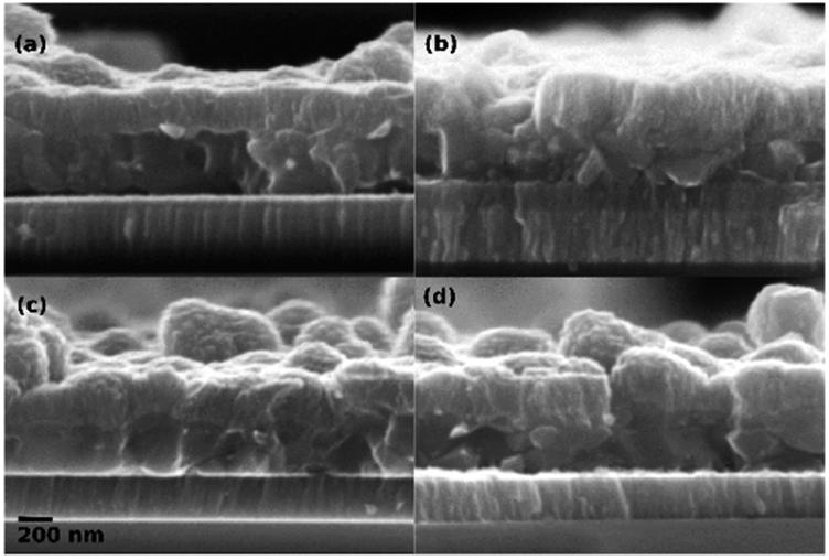 | ||
| Fig. 5 Cross-section of devices with absorber thickness of about 250 nm. (a) No passivation layer and no NaF. (b) No passivation layer and NaF deposited onto CZTS precursor before annealing. (c) Al2O3 passivation and NaF deposited onto CZTS precursor prior to annealing. (d) HfO2 passivation layer and NaF deposited onto CZTS precursor prior to annealing. | ||
In conclusion, the attempts to use NaF to allow charge transport through 5 nm Al2O3 or HfO2 was successful. Earlier studies on CIGS showed that selenization of dielectric passivation layers in the presence of NaF resulted in the creation of contact openings, which allowed charge transport through to the back contact. In line with these results, we observe that devices where NaF was deposited onto the precursor prior to annealing resulted in non-blocked devices with 5 nm Al2O3 or HfO2 passivation layers. If NaF was not used, the devices with HfO2 were blocked, while the sample with Al2O3 delaminated. It was furthermore found that NaF deposited onto the passivation layer before CZTS precursor sputtering was problematic in most cases due to higher risk of absorber delamination. NaF deposited onto the precursor resulted in fewer delamination issues. The NaF still clearly affects the back contact in this case by catalysing MoS2 formation. It is therefore conceivable that NaF also affects the passivation layer, by creation of openings in a similar fashion as previously seen for CIGS.
Discussion and outlook
The results in this work with relatively small losses in performance for CZTS devices with reducing thickness even to 250 nm is encouraging, but the efficiency is still too low for many applications such as a tandem top cell. A comparison of device performance as a function of band gap energy and absorber thickness for CIGS and CZTS devices is shown in Table 3. For thick devices with band gap energies around 1.6 eV, CZTS has only slightly lower JSC and FF as compared to CuGaSe2 (CGS) and Ag-CIGS (ACIGS), but the VOC deficit is larger. For thin devices, band gap energies vary, making comparisons difficult. However, it can be seen that despite a relatively decent performance for very thin CZTS absorbers, the high VOC deficit as compared to the band gap energy is limiting these devices as compared to CIGS. It can also be seen that the loss in performance with thickness reduction is lower for CZTS as compared to CIGS.| Material | Thickness [nm] | E g [eV] | V OC [mV] | J SC [mA cm−2] | FF [%] | Eff. [%] | Ref. |
|---|---|---|---|---|---|---|---|
| CIGS | 300 | 1.3 | 666 | 20.7 | 68.7 | 9.5 | 32 |
| CIGS | 490 | 1.25 | 733 | 26.4 | 78.2 | 15.2 | 33 |
| CIGS | 2000 | 1.1 | 734 | 39.6 | 80.4 | 23.3 | 34 |
| ACIGS | 2100 | 1.63 | 891 | 16.0 | 66.8 | 9.5 | 4 |
| CGS | 1000 | 1.64 | 1017 | 17.5 | 67 | 11.9 | 5 |
| CZTS | 1.5 | 730 | 21.7 | 69.3 | 11.0 | 35 | |
| CZTS | 1200 | 1.64 | 801 | 15.8 | 64.8 | 7.1 | 21 |
| CZTS* | 250 | 1.53 | 626 | 17.0 | 52.5 | 5.6 | This work |
| CZTS* | 300 | 1.48 | 598 | 16.5 | 62.6 | 6.2 | This work |
| CZTS | 380 | 1.52 | 673 | 16.0 | 63.8 | 6.9 | This work |
| CZTS* | 400 | 658 | 19.8 | 65.9 | 8.6 | 8 |
The band gap energy of CZTS can be varied depending on the degree of cation disorder.36 In our work, band gap energies obtained from optical measurements or extracted from QE have been found to vary between 1.4 to 1.6 eV depending on the degree of order.19,37 For a 2-terminal tandem on Si, an increase of the band gap energy closer to 1.7 eV would be optimal.6 One way of increasing the band gap energy is by alloying with germanium. For pure sulphides, a Ge/(Ge + Sn) content of around 0.2–0.4 is needed to give a band gap energy of 1.7 eV.38 In our previous work, issues with delamination of Ge-containing films during etching and chemical bath deposition of CdS hindered fabrication of devices. Introduction of adhesive TiN layers between Mo and CZGS improved adhesion, but only CZGS absorbers were fabricated, not alloyed CZGTS.39 The conduction band alignment between CdS and CZTS is known to be non-ideal (negative), and to be even worse with Ge-alloying since most of the band gap increase with Ge-alloying is in the conduction band. In ref. 39, we showed that exchange of CdS with ZnSnO by atomic layer deposition gives increased VOC for CZGS devices, with voltages of up to 1.1 V. Since the band gap energy and position of the conduction band can be tuned for ZTO, optimisation of this buffer layer for alloyed CZGTS with band gap energy around 1.7 eV should be possible and is recommended for future work. This could also be combined with the use of Al2O3 back contact passivation layers including NaF treatment as shown in this work to optimise the back contact. The back contact also needs to be transparent and future work is needed to reach the same performance for devices as on Mo back contacts. Further mitigation of voltage losses from bulk recombination will also be needed to reach the efficiency required from a top cell.
Conclusions
CZTS devices with varying thickness down to 250 nm were fabricated and compared to previous thickness studies. Efficiencies of around 6% were achieved for these thin devices. The performance loss for thickness reduction in CZTS is smaller than for CIGS, and part of the explanation is that the diffusion length in CZTS is smaller. It is also possible that optimisation of the 2-step processing used for CZTS is simplified for thin absorbers. Some improvements can be seen for addition of thin backside passivation layers, but the majority of the VOC deficit remains. The use of NaF treatment for making Al2O3 passivation layers conductive is demonstrated for CZTS.Conflicts of interest
There are no conflicts to declare.Acknowledgements
The authors acknowledge financial support from the Swedish Foundation for Strategic Research (grant no. RMA15-0030) and the Swedish Research Council (grant no. 2019-04793 and 2020-04065). This work has also received funding from the European Union’s Horizon 2020 Research and Innovation Programme under grant agreement no. 952982 (Custom-Art project).Notes and references
- M. A. Green, E. D. Dunlop, J. Hohl-Ebinger, M. Yoshita, N. Kopidakis and X. Hao, Prog. Photovoltaics, 2022, 30(1), 3, DOI:10.1002/pip.3506.
- S. Essig, C. Allebé and T. Remo, et al. , Nat. Energy, 2017, 2, 17144, DOI:10.1038/nenergy.2017.144.
- Y. Romanyuk, S. Haas, S. Giraldo, M. Placidi, D. Tiwari, D. Fermin, X. Hao, H. Xin, T. Schnabel and M. Kauk-Kuusik, JPhys Energy, 2019, 1, 044004, DOI:10.1088/2515-7655/ab23bc.
- J. Keller, L. Stolt, K. V. Sopiha, J. K. Larsen, L. Riekehr and M. Edoff, Sol. RRL, 2020, 4(12), 2000508, DOI:10.1002/solr.202000508.
- F. Larsson, N. Shariati Nilsson, J. Keller, C. Frisk, V. Kosyak, M. Edoff and T. Törndahl, Prog. Photovoltaics, 2017, 25(9), 755, DOI:10.1002/pip.2914.
- S. R. Kurtz, P. Faine and J. M. Olson, J. Appl. Phys., 1990, 68, 1890, DOI:10.1063/1.347177.
- K. Kim, J. Gwak, S. Kyu Ahn, Y.-J. Eo, J. Hyung Park, J.-S. Cho, M. Gu Kang, H.-E. Song and J. Ho Yun, Sol. Energy, 2017, 145, 52, DOI:10.1016/j.solener.2017.01.031.
- F. Liu, J. Huang, K. Sun, C. Yan, Y. Shen, J. Park, A. Pu, F. Zhou, X. Liu, J. A. Stride, M. A. Green and X. Hao, NPG Asia Mater., 2017, 9, e401, DOI:10.1038/am.2017.103.
- Y. Ren, J. J. S. Scragg, C. Frisk, J. K. Larsen, S.-Y. Li and C. Platzer-Björkman, Phys. Status Solidi A, 2015, 212, 2889, DOI:10.1002/pssa.201532311.
- F. Martinho, A. Hajijafarassar, S. Lopez-Marino, M. Espindola-Rodriguez, S. Engberg, M. Gansukh, F. Stulen, S. Grini, S. Canulescu, E. Stamate, A. Crovetto, L. Vines, J. Schou and O. Hansen, ACS Appl. Energy Mater., 2020, 3(5), 4600, DOI:10.1021/acsaem.0c00280.
- B. Vermang, Y. Ren, J. Joel, C. Frisk, O. Donzel-Gargand, P. Salome, J. Borme, S. Sadewasser, C. Platzer-Bjorkman and M. Edoff, IEEE J. Photovolt., 2016, 6(1), 332, DOI:10.1109/jphotov.2015.2496864.
- S. Englund, T. Kubart, J. Keller, M. V. Moro, D. Primetzhofer, S. S. Suvanam and C. Platzer Björkman, Phys. Status Solidi A, 2019, 216(22), 1900542, DOI:10.1002/pssa.201900542.
- S. Englund, S. Grini, O. Donzel-Gargand, V. Paneta, V. Kosyak, D. Primetzhofer and C. Platzer Björkman, Phys. Status Solidi A, 2018, 215(23), 1800491, DOI:10.1002/pssa.201800491.
- S. Englund, V. Paneta, D. Primetzhofer, Y. Ren, O. Donzel-Gargand, J. K. Larsen and C. Platzer Björkman, Thin Solid Films, 2017, 639, 91, DOI:10.1016/j.tsf.2017.08.030.
- D. Ledinek, O. Donzel-Gargand, M. Sköld, J. Keller and M. Edoff, Sol. Energy Mater. Sol. Cells, 2018, 187, 160, DOI:10.1016/j.solmat.2018.07.017.
- G. Birant, et al. , Sol. Energy, 2020, 207, 1002, DOI:10.1016/j.solener.2020.07.038.
- G. Birant, et al. , EPJ Photovoltaics, 2020, 11, 10, DOI:10.1051/epjpv/2020007.
- J. K. Larsen, J. J. Scragg, C. Frisk, Y. Ren and C. Platzer-Björkman, Phys. Status Solidi A, 2015, 212, 2843, DOI:10.1002/pssa.201532420.
- J. K. Larsen, et al. , Adv. Energy Mater., 2019, 9(21), 1900439, DOI:10.1002/aenm.201900439.
- J. Lindahl, et al. , IEEE J. Photovolt., 2013, 3(3), 1100, DOI:10.1109/jphotov.2013.2256232.
- J. K. Larsen, F. Larsson, T. Törndahl, N. Saini, L. Riekehr, Y. Ren, A. Biswal, D. Hauschild, L. Weinhardt, C. Heske and C. Platzer-Björkman, Adv. Energy Mater., 2019, 1900439, DOI:10.1002/aenm.201900439.
- C. Frisk, Y. Ren, S.-Y. Li and C. Platzer-Björkman, IEEE 42nd Photovoltaic Specialist Conference (PVSC). Proceedings IEEE conference, 2015, DOI:10.1109/pvsc.2015.7355794.
- S.-Y. Li, C. Hägglund, Y. Ren, J. J. S. Scragg, J. K. Larsen, C. Frisk, K. Rudisch, S. Englund and C. Platzer-Björkman, Sol. Energy Mater. Sol. Cells, 2016, 149, 170, DOI:10.1016/j.solmat.2016.01.014.
- C. Frisk, T. Ericson, S.-Y. Li, P. Szaniawski, J. Olsson and C. Platzer-Björkman, Sol. Energy Mater. Sol. Cells, 2016, 144, 364, DOI:10.1016/j.solmat.2015.09.019.
- J. Ge, J. Chu, Y. Yan, J. Jiang and P. Yang, ACS Appl. Mater. Interfaces, 2015, 7, 10414 CrossRef CAS PubMed.
- S. Englund, T. Kubart, J. Keller, M. V. Moro, D. Primetzhofer, S. S. Suvanam, J. J. S. Scragg and C. Platzer-Björkman, Phys. Status Solidi A, 2019, 216, 1900542, DOI:10.1002/pssa.201900542.
- N. Barreau and J. C. Bernède, J. Phys. D: Appl. Phys., 2002, 35(11), 1197, DOI:10.1088/0022-3727/35/11/316.
- J.-G. Song, et al. , Nanotechnology, 2017, 28, 465103, DOI:10.1088/1361-6528/aa8f15.
- P. Yang, et al. , Nat. Commun., 2018, 9, 979, DOI:10.1038/s41467-018-03388-5.
- K.-J. Yang, et al. , Prog. Photovoltaics, 2015, 23(7), 862, DOI:10.1002/pip.2500.
- K. Wang, et al. , Appl. Phys. Lett., 2010, 97(14), 143508, DOI:10.1063/1.3499284.
- J. Pettersson, T. Törndahl, C. Platzer-Björkman, A. Hultqvist and M. Edoff, IEEE J. Photovolt., 2013, 3(4), 1376, DOI:10.1109/jphotov.2013.2276030.
- L. M. Mansfield, A. Kanevce, S. P. Harvey, K. Bowers, C. Beall, S. Glynn and I. L. Repins, Prog. Photovoltaics, 2018, 26(11), 949, DOI:10.1002/pip.3033.
- M. Nakamura, K. Yamaguchi, Y. Kimoto, Y. Yasaki, T. Kato and H. Sugimoto, IEEE J. Photovolt., 2019, 9(6), 1863, DOI:10.1109/jphotov.2019.2937218.
- K. Sun, C. Yan, F. Liu, J. Huang, F. Zhou, J. A. Stride, M. Green and X. Hao, Adv. Energy Mater., 2016, 1600046, DOI:10.1002/aenm.201600046.
- J. J. S. Scragg, J. K. Larsen, M. Kumar, C. Persson, J. Sendler, S. Siebentritt and C. Platzer Björkman, Phys. Status Solidi B, 2016, 253(2), 247, DOI:10.1002/pssb.201552530.
- Y. Ren, N. Ross, J. K. Larsen, K. Rudisch, J. J. S. Scragg and C. Platzer-Björkman, Chem. Mater., 2017, 29, 3713–3722, DOI:10.1021/acs.chemmater.7b00671.
- N. Saini, J. K. Larsen, K. V. Sopiha, J. Keller, N. Ross and C. Platzer-Björkman, Phys. Status Solidi A, 2019, 216, 1900492, DOI:10.1002/pssa.201900492.
- N. Saini, N. M. Martin, J. K. Larsen, A. Hultqvist, T. Törndahl and C. Platzer-Björkman, Sol. RRL, 2022, 6(2), 2100837, DOI:10.1002/solr.202100837.
Footnote |
| † Electronic supplementary information (ESI) available. See https://doi.org/10.1039/d2fd00052k |
| This journal is © The Royal Society of Chemistry 2022 |