
 Open Access Article
 This Open Access Article is licensed under a Creative Commons Attribution-Non Commercial 3.0 Unported Licence
Shape-tailored semiconductor dot-in-rods: optimizing CdS-shell growth for enhanced chiroptical properties via the rationalization of the role of temperature and time†
Junjie
Hao‡
 abe,
Peizhao
Liu‡
ch,
Ziming
Zhou‡
c,
Haochen
Liu‡
c,
Wei
Chen
cdf,
Peter
Müller-Buschbaum
fg,
Jiaji
Cheng
h,
Kai
Wang
c,
Xiao Wei
Sun
*c,
Jean-Pierre
Delville
*b and
Marie-Helene
Delville
*a
abe,
Peizhao
Liu‡
ch,
Ziming
Zhou‡
c,
Haochen
Liu‡
c,
Wei
Chen
cdf,
Peter
Müller-Buschbaum
fg,
Jiaji
Cheng
h,
Kai
Wang
c,
Xiao Wei
Sun
*c,
Jean-Pierre
Delville
*b and
Marie-Helene
Delville
*a
aUniv. Bordeaux, CNRS, Bordeaux INP, ICMCB, UMR 5026, F-33600 Pessac, France. E-mail: marie-helene.delville@icmcb.cnrs.fr
bUniv. Bordeaux, CNRS, LOMA, UMR 5798, 33405 Talence, France
cInstitute of Nanoscience and Applications, Department of Electrical and Electronic Engineering, Southern University of Science and Technology, Shenzhen, 518055, China
dCollege of Engineering Physics, Shenzhen Technology University, Shenzhen, 518118, China
eCollege of Integrated Circuits and Optoelectronic Chips, Shenzhen Technology University, Shenzhen, 518118, China
fTechnical University of Munich, TUM School of Natural Sciences, Department of Physics, Chair for Functional Materials, James-Franck-Str. 1, 85748 Garching, Germany
gHeinz Maier-Leibnitz Zentrum (MLZ), Technical University of Munich, Lichtenbergstraße 1, 85748 Garching, Germany
hKey Laboratory for the Green Preparation and Application of Functional Materials, Ministry of Education, School of Materials Science and Engineering, Hubei University, Wuhan, 430062, China
First published on 29th January 2025
Abstract
Colloidal chemistry provides an assortment of synthetic tools for tuning the shape of semiconductor nanocrystals. To fully exploit the shape- and structure-dependent properties of semiconductor nanorods, high-precision control on growth and design is essential. However, achieving this precision is highly challenging due to the high temperatures (>350 °C) and short reaction times (<8 minutes) often required for these reactions. In this study, we performed the first investigation on the impact of temperature and time on the CdS-shell growth of CdSe/CdS quantum rods. Our findings demonstrate that temperature plays a pivotal role in achieving ultra-thin shell dot-in-rods, which are crucial for enhancing chiroptical properties. The two-step process proposed here explains the shell growth of CdSe/CdS dot-in-rods (DRs). It involves finely-tuned isotropic shell growth in the first stage, followed by anisotropic length growth along the [0001] rod axis in the second step. This approach has two advantages: a systematic control of the shell thickness for different aspect ratios (ARs) and batch monodispersity. These DRs, with an ultra-thin CdS shell and a high AR, after modification with L/D cysteine molecules, exhibit significant enhancement of their ligand-induced chirality, with circular dichroism (CD) g-factor values as high as 10−3.
1 Introduction
The induction of optical activity in colloidal semiconductor nanocrystals (NCs) is a promising way to expand the list of their properties and to enable their use in stereoselective synthesis,1–3 chiral recognition,4,5 display devices,6,7 biosensing,8,9 asymmetric catalysis,10 and so on.11–13 Among these properties, chirality remains at the core of intense research, particularly when dealing with the ground and excited electronic (emissive) states of quantum dots (QDs).2,14–17 Gun'ko was among the first to report the circular dichroism (CD) response of CdS QDs capped with chiral molecules.18 This chirality in QDs arises from mechanisms as different as the use of a chiral shell layer,18–21 the presence of chiral dislocations and defects,3,22,23 ligand-induced chirality,16,24,25 and chiral assemblies.2,26–28 Among all these mechanisms, ligand exchange with chiral molecules has driven significant progress not only in producing QDs with uniform size distribution but also in designing their surface chemistry to impart the targeted chemical properties. Circularly polarized luminescence (CPL), the counterpart of CD in terms of emission, has been reported in few studies; only spherical and rod-shaped semiconductor NC samples with chiral–ligand-induced CPL have been reported,15,16,29,30 where L- and D-cysteine play a central role in CD and CPL performances. The regulation of these optical phenomena by the CdSe/CdS QD morphologies and sizes has been achieved in recent years,17,31,32 showing the importance of the presence and the thinness of the CdS layer on the core surface.32 Indeed, the versatility of inorganic nanocrystals (NCs) has been extended significantly, thanks to the ability to tweak their electronic properties by changing their size and dimensionality (high level of fluorescence anisotropy and enhanced potential for electron–hole separation).33–36CdSe/CdS dot-in-rods (DRs) are visible light-emitting nanocrystals that form robust systems combining a high degree of monodispersity with bright and narrow photoluminescence.37–39 However, although rapid initial progress in their development has resulted in the achievement of DRs with different aspect ratios (ARs) and colors in the visible range,40–46 improvements in the control of their morphology at the nanoscale, using conventional fast-injection-based preparations, are still under development. This is especially true for the control of a targeted ultra-thin shell.
Even if such thin shells have a positive influence on the improvement of catalytic performances47 and chirality,17,24,32 to the best of our knowledge, no investigation so far has directly focused on the synthesis of uniform quantum rods that can combine thin shells with varying ARs. Only a few publications mentioned the control of the DR shell thickness. Bawendi38 used a second over-coating process and focused on DRs with thicker shells to enhance the quantum yield (QY) to nearly 100%. She et al.48 studied the QYs and photophysical processes by systematically tuning the shell and seed sizes, including the thin shell case, but in fact, both the shell layer and length increased simultaneously. Kim et al.40 proposed a dual-diameter structure for these semiconductor nanorods exhibiting two distinctly segmented parts with different diameters and a thicker shell on the CdSe seed. Khon et al.47 obtained thin-shell DRs by etching a 0.7 nm CdS layer from the CdSe/CdS nanorods, enhancing their catalytic activity more than 3 times compared to the original CdSe/CdS DRs.
Additionally, when considering the impact of shell thickness variation on the chiral properties of CdSe/CdS nanorods, two competing effects should be taken into account: (i) the CdS shell acts as an energy barrier for holes within the CdSe core, potentially hindering their chiral electronic coupling with surface ligands and leading to a decrease in CD signals; (ii) conversely, appropriately designed CdS layers can lower the energy of holes, bringing them closer to the energetic resonance of the Highest Occupied Molecular Orbital (HOMO) of the ligand. This closer alignment enhances the CD responses, as it facilitates stronger interactions between holes and ligands. Therefore, the limitations in chirality transfer via the post-ligand exchange strategy remain to be fully understood. Nonetheless, these examples highlight the critical importance of thin shell thickness for achieving high CD and CPL activities. They also show the complexity of achieving such high-precision control in the synthesis of DRs when increasing their lengths and ARs. Obtaining DRs with both a high AR and a thin shell is a prerequisite for studying, controlling, and even increasing their ligand-induced CD and CPL activities.
Therefore in this work, we aimed to first analyse and understand the discrepancies in the literature concerning the temperature and time reaction conditions, then address the two issues mentioned above, and determine how thin the shell of a DR should be for optimal optical properties. To do so, we reinvestigated and modeled (1) the variation of the DRs' dimensions with time, (2) the effect of temperature throughout the synthesis on the DRs' shell thickness and (3) the effect of seed concentration on the aspect ratio of the thin-shell DRs. We eventually checked the influence of shell thickness on the chirality of asymmetric DRs.
2 Experimental section
2.1 Characterization
The TEM pictures were taken using an FEI Tecnai G2 F30 microscope (300 kV), Talos F200X G2 (200 kV) (Shenzhen), or a JEOL 2200 FS equipped with a field emission gun, operating at 200 kV and with a point resolution of 0.23 nm (Pessac). HRTEM micrographs were acquired with a GatanUltrascan CCD 2k–2k and digital diffractograms were calculated using the Gatan Digital Micrograph program. The UV/vis absorption measurements were performed using a TU-1901 double-beam UV/vis spectrophotometer (Beijing Purkinje General Instrument Co. Ltd, China), and the photoluminescence (PL) spectra were recorded on a fluoroSENS spectrophotometer (Gilden Photonics).All the heating mantles are made by Glas-Col but have different setups. (1) Typically, the experiments were performed by using a 180 W Series O spherical mantle (high capacity) covering both the top and the bottom of the flask to improve safety and efficiency; (2) we chose the 50% (90 W) input power controlled by the Glas-Col controller of lower power for control experiments, which decreases the heating rate (from ∼12 K min−1 to ∼5 K min−1).
2.2 Synthetic procedures
![[thin space (1/6-em)]](https://www.rsc.org/images/entities/char_2009.gif) :TOP solution (0.4 mL, 1 mol L−1) was injected at 653 K and reacted for several seconds. The size of the CdSe seed could be adjusted by altering the temperature, Cd:Se ratio, reaction time, and type of phosphonic acid (ODPA or TDPA).
:TOP solution (0.4 mL, 1 mol L−1) was injected at 653 K and reacted for several seconds. The size of the CdSe seed could be adjusted by altering the temperature, Cd:Se ratio, reaction time, and type of phosphonic acid (ODPA or TDPA).
Purification of the CdSe-TOP seed. The reaction mixture was cooled to 343–353 K and mixed with 50 μL (40.85 mg) of TBP; then 4 mL of ethanol was added to the above solution, which was centrifuged at 10000 rpm for 3 minutes. Then, the precipitate was dissolved in a small amount of toluene while the supernatant was discarded. After centrifugation again, the precipitate was dissolved in TOP (CdSe-TOP). Due to the TBP purification process, the CdSe seed can be better purified, removing the adsorbed ions on the surface and the by-products in the solution. This is essential for achieving uniform morphology control and high quantum yield in DRs.
:TOP (0.5 mL, 2.5 mol L−1) and the above CdSe-TOP solution (100 μL) were injected into the flask. After injection, the temperature dropped to 543–573 K and then recovered to the pre-injection temperature within two minutes. The CdSe/CdS DRs were allowed to grow for approximately 8 minutes after the injection. Finally, the reaction mixture was cooled to room temperature, and the nanocrystals were separated from the side products and unreacted precursors using the same purification procedure as for the CdSe seed, except for the addition of TBP. After the reaction completion, a hair dryer was used to achieve rapid cooling and reduce the temperature by more than 100 K within the first minute, thereby effectively stopping the growth of CdSe/CdS DRs.
The shell thickness can be controlled by changing the injection temperature, heating mantle power, or ambient temperature. CdSe/CdS DRs with different aspect ratios were also synthesized by adjusting the seed concentration and reaction time.
3 Results and discussion
An analysis of the various syntheses proposed by various groups in the literature (Fig. 1 and Table 1) shows that the control of the shell thickness of these DRs is rather difficult and drastically depends on the temperatures and the working conditions. Based on these results, it was shown that temperature indeed played a major role at different stages of the synthesis, from room temperature to injection. Table 1 summarizes all the details, while Fig. 1 provides a quick overview of the detrimental effect of the temperature on the shell thickness. The control of the CdSe/CdS DRs' shell thickness is poor at such high injection temperatures, and the results may vary widely (Fig. 1 and Table 1) (as many as eight thicknesses could be obtained for one single temperature: 623 K).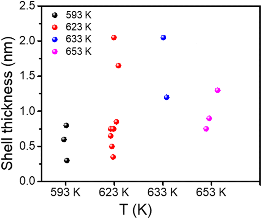 | ||
| Fig. 1 Range of shell thicknesses of CdSe/CdS DRs for given temperatures and a reaction time of 8 min based on data from Table 1. | ||
| No. | λ Abs (nm) | Seed diam. (nm) | T injection (K)/time (min) | DR length (nm) | DR diam. (nm) | DR AR | Shell-thickness (nm) | Ref. |
|---|---|---|---|---|---|---|---|---|
| a Diameter of the CdSe seed determined from the absorption spectrum using Peng's equation (nm);54 b The ambient temperature was 303 K (summertime). c The ambient temperature was 291 K (wintertime); reaction time: 8 min, otherwise indicated. | ||||||||
| 1 | — | 3.2 | 623 | 53 ± 4 | 3.9 ± 0.2 | 13.6 | 0.35 | 41 |
| 2 | 3.3 | 623 | 35 ± 2 | 4.2 ± 0.4 | 8.3 | 0.50 | 41 | |
| 3 | 3.3 | 653 | 19 ± 1 | 5.0 ± 0.5 | 3.8 | 0.90 | 41 | |
| 4 | 585 | 4.0a | 623/10 | 44 ± 4 | 5.5 ± 0.2 | 8.0 | 0.75 | 38 |
| 5 | — | 3.9a | 638 | 28 ± 4 | 8 ± 1 | 3.5 | 2.05 | 49 |
| 6 | 3.4a | 623 | 44 ± 8 | 4.9 ± 0.7 | 9.0 | 0.75 | 49 | |
| 7 | 3.1a | 623 | 108 ± 25 | 4.6 ± 0.5 | 23.5 | 0.75 | 49 | |
| 8 | — | 3.4a | 653 | 37 ± 3 | 4.9 ± 0.6 | 7.6 | 0.75 | |
| 9 | 2.9a | 633 | 56 ± 3 | 5.3 ± 0.6 | 10.6 | 1.20 | 50 | |
| 10 | 536 | 2.7 | 623/20 | 22 | 7 | 3.1 | 2.15 | 45 |
| 11 | 623 | 22 | 4 | 5.5 | 0.65 | 45 | ||
| 12 | 653/20 | 35 | 7 | 5.0 | 2.15 | 45 | ||
| 13 | 623/40 | 58 | 7 | 8.3 | 2.15 | 45 | ||
| 14 | — | 4.2 | 623 | 42 | 7.5 | 5.6 | 1.65 | 45 |
| 15 | — | 3.5 | 623/6 | 24.0 ± 2 | 5.0 ± 0.5 | 4.8 | 0.75 | 51 |
| 16 | 557 | 3.2a | 623 | 36.5 | 7.3 | 5.0 | 2.05 | 52 |
| 17 | — | 4.2 | 593 | 49 ± 2.5 | 5.8 ± 0.5 | 8.4 | 0.8 | 53 |
| 18 | 653b | 30.4 ± 2.5 | 5.8 ± 0.8 | 5.2 | 1.3 | This work | ||
| 19 | 623b | 32.5 ± 2.0 | 4.9 ± 0.5 | 6.6 | 0.85 | This work | ||
| 20 | 593b | 24.3 ± 1.6 | 3.8 ± 0.4 | 6.4 | 0.35 | This work | ||
| 21 | 593c | 24.5 ± 2.0 | 4.4 ± 0.5 | 5.6 | 0.6 | This work | ||
To clarify the discrepancies between these results, we performed all the experiments with a temperature control located directly inside the solution to ensure more accurate monitoring of the reaction. Room-temperature solution injections were introduced into the solution only after it had reached and stabilized at the desired temperature.
We then decided to reinvestigate the growth of CdSe/CdS DRs by varying (i) the reaction time to follow the involved mechanisms, (ii) the reaction temperature to determine activation energies and optimize the AR range, and (iii) the concentration of CdSe seeds to offer even more versatility in the AR.
Typically, 3.2 nm wurtzite (WZ)-CdSe seeds54 were chosen as starting seed samples (λabs = 557 nm, Fig. S1†) to study the growth process over a wide range of reaction times from 30 s to 16 min, with reaction temperatures extending from 503 to 653 K, and seed concentrations ranging from 4 to 40 μM.
3.1 Variation of the size of DRs with the reaction time
Peng et al.55 investigated the growth of CdSe nanorods (NRs) and interpreted their data considering three main stages. (i) Initially, the ‘spherical’ CdSe nanocrystals grow isotropically; (ii) after a certain time, likely related to the development of well-defined facets, the so-called one-dimensional growth (1D) emerges when the axial growth rate is much higher than the almost negligible radial one; (iii) after another characteristic time, the NR growth becomes three-dimensional (3D), with growth occurring in both axial and radial directions. They mentioned that, during growth, NRs can also undergo some reshaping, which they attribute to the surface-to-bulk energy ratio that reduces the AR with little influence on the growth itself, as illustrated by the increase in NRs' volume.Here we performed the first set of experiments starting from the same CdSe seed (Ds = 3.2 nm) at a concentration of 14 μM, and at 593 K. We varied the time and analysed the growth of the resulting CdSe/CdS DRs. Fig. 2 illustrates the precise control of their morphology, and Table 2 provides detailed information on the variation of the CdS shell thickness (D − Ds/2), the overall length of the DRs (L), their overall aspect ratios (AR = L/D), and the increase in the overall volume with time.
 | ||
| Fig. 2 TEM images of DRs (DR-1 to DR-6) synthesized under different reaction times starting with the same CdSe seed solution (Ds = 3.2 nm) at a concentration of 14 μM. (a) 30 s, (b) 60 s, (c) 120 s, (d) 240 s, (e) 480 s, and (f) 960 s. | ||
| Name | React time (s) | Length L (nm) | D (nm) | AR L/D | Shell-thickn. (D − Ds)/2 (nm) | V (nm3) |
|---|---|---|---|---|---|---|
| a Overall volume V = πD2(L − D/3)/4, assuming a cylindrical part with hemispherical ends. | ||||||
| DR-1 | 30 | 5.5 ± 0.9 | 3.4 ± 0.5 | 1.6 | 0.1 | 39.6 |
| DR-2 | 60 | 8.0 ± 1.0 | 3.6 ± 0.5 | 2.2 | 0.2 | 69.2 |
| DR-3 | 120 | 15.7 ± 3.0 | 3.6 ± 0.4 | 4.4 | 0.2 | 147.6 |
| DR-4 | 240 | 21.7 ± 2.7 | 3.8 ± 0.4 | 5.7 | 0.3 | 223.8 |
| DR-5 | 480 | 38.7 ± 3.5 | 3.6 ± 0.4 | 10.8 | 0.35 | 381.4 |
| DR-6 | 960 | 35.8 ± 2.4 | 5.4 ± 0.8 | 6.6 | 1.1 | 778.7 |
As (i) the morphology of nanorods can be described as a cylindrical part with two hemispherical tips and (ii) cylinders and spheres have different symmetries, the growth law of the overall length L involves both axial and radial components. Then, we separate them considering that a NR, of overall length L and diameter D, can be described as a cylindrical part of length l = L − D capped by two hemispherical tips of radius D/2. Fig. 3 shows a diagram of such a nanorod, depicting the growth sequence of the length (l), diameter (D), volume (V − Vseed) of the grown CdS material, and the aspect ratio, now defined as l/D (l/D = L/D − 1) to explicitly separate symmetries, for the seeded case where CdS grows over a CdSe seed at T = 593 K; raw data corresponding to this growth are provided in Table 2.
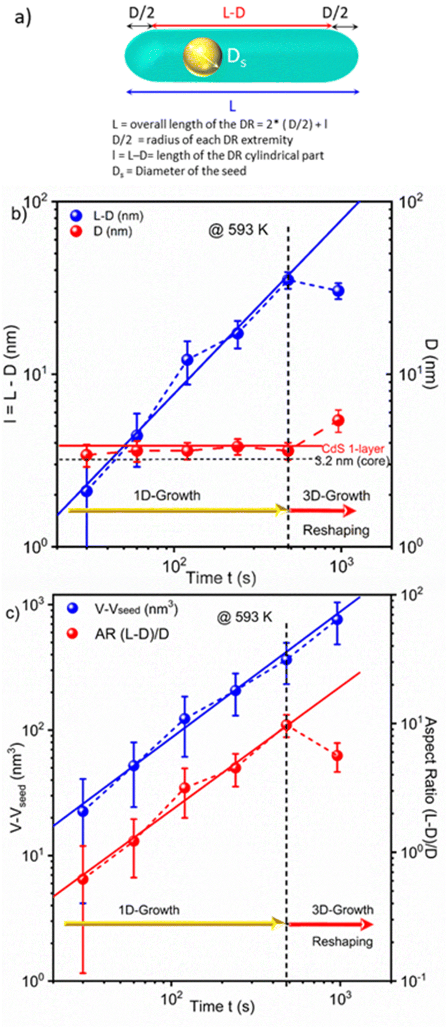 | ||
| Fig. 3 (a) Schematic of a DR (dot in a rod) with all the distances used in the manuscript. (b) Linear variation of the length (l = L − D) on the cylindrical part with time. Note that the diameter D remains constant (1D-growth); 3D growth and/or reshaping occurs after a reaction time onset of around 8 minutes under the present experimental conditions. (c) Linear variation of the CdS DR volume (V − Vseed) and the cylindrical-to-spherical aspect ratio (l/D) with time; the persistence of the linear variation of the volume of CdS beyond 8 minutes (480 s: vertical dotted line) suggests a DR reshaping. CdSe seed (3.2 nm) at a concentration of 14 μM and T = 593 K; see text for the data fitting. | ||
Schematically, the growth of DRs starting from the 3.2 nm seeds in the presence of ligands grafted on the surface shows the following stages, analogous to those observed by Peng under seedless conditions.55 (i) When starting with polyhedron CdSe seeds of nearly spherical symmetry, the growth of a CdS layer on a seed remains isotropic until the emergence of facets that differentiate the surface energy properties (one CdS layer seems sufficient to induce such a differentiation). (ii) When this difference in surface energy becomes high enough,56 the asymmetric growth is triggered along the axial direction. DRs form (1D-growth), and a maximum overall aspect ratio of 10 can be reached. (iii) Eventually, these DRs undergo 3D growth with some reshaping, likely to minimize surface energy stresses in comparison to bulk ones. This reshaping is evidenced by the concomitant decrease in length observed in Fig. 3b, and by the continuous volume growth with the reaction time, as shown in Fig. 3c.
The growth kinetic mechanisms of II–VI semiconductor DRs are not yet well established, particularly for the 1D-growth regime. On the one hand, Viswanatha et al.57 investigated in detail the growth of bare CdS spherical nanoparticles during the Ostwald ripening regime and experimentally confirmed the validity of a diffusion-limited growth mechanism in this case. On the other hand, the growth mechanism of ligand-capped spherical CdSe nanoparticles remains a topic of debate. While half of the studies propose a diffusion-limited interpretation,58,59 the other half suggests a reaction-limited mechanism.60,61
Nonetheless, when looking at the broader literature concerning the growth of metallic-capped nanoparticles, particularly gold ones62 (see also references therein), it looks like the growth of ligand-capped gold nanoparticles may follow different consecutive steps and mechanisms, but they are all driven by a surface reaction-limited process. Then, following these lines and considering the symmetry of the DRs, we examine the growth of the cylindrical part and the hemispherical tips separately.
For reaction-limited growth on CdSe seeds, well before the final Ostwald ripening, i.e., in the free-growth regime during which the solute concentration at infinity ([C]∞) can be assumed constant, the growth of the DRs can be qualitatively obtained by balancing the DR volume growth rate with the reactive flux (Jreac) at the concerned surface of the DR.
Thus, axial growth occurs from the reaction flux at the spherical tips (index s) of the DRs such that we have dV/dt|D = VM·Jreacs = VM·πD2ks[C]∞, whereas radial growth occurs from the reaction flux at the cylindrical part (index c) of the DRs so that dV/dt|l = VM·Jreacc = VM·πDlkc[C]∞, where VM is the molar volume of CdS and ks,c represents the reaction rates for solute incorporation into the DRs; ks,c is classically expressed in nm s−1.62 Using the volume V = πD2(l + 2D/3)/4 of a DR, we, thus, expect the following growth rates (eqn (1)):
 | (1) |
Moreover, in this 1D-growth regime, the volume of the DRs corrected by the volume of the seed (V1d − Vseed), i.e., the amount of grown material, and the aspect ratio, AR1d = l1d/D1d, are also expected to behave respectively as (V1d − Vseed)(t) ≈ πl1d(t)D021d/4 = πD021dVMks[C]∞t and AR1d(t) = l1d(t)/D01d ≈ 4VMks[C]∞t/Ds, both linearly varying with time. This is experimentally determined and again confidently fitted using power-laws with respective exponents of 1.006 and 0.96 and correlations of 0.99 and 0.98. Note also that a linear fit of (V1d(t) − Vseed) ≈ πl1d(t)D021d/4 as a function of l1d before reshaping, gives a slope of πD021d/4 = (12.14 ± 0.22) nm2, from which we can deduce a statistical average diameter of D01d = (3.93 ± 0.04) nm during the 1D-growth phase. This value corresponds to the seed diameter, Ds = 3.2 nm covered with a single CdS layer (≈0.35 nm) and, thus, strongly supports the fact that the first transitory isotropic growth stage of CdS onto the spherical CdSe seeds involves the growth of just a monolayer of CdS to trigger the 1D-growth. We finally note that DRs eventually reshape when their overall aspect ratio reaches a maximum value of (l1d/D1d + 1) ≈ 11 under the present experimental conditions. However, this reshaping does not affect the growth as illustrated by the continued linear variation of the DR volume with time, despite the decrease in their length.
This dynamic thus suggests a method to consistently produce high aspect ratio NRs with the thin-shell thickness remaining around 1 CdS monolayer as long as the growth remains within the 1D-regime, i.e., up to a reaction time of 8 minutes under the present experimental conditions. Indeed, for longer reaction times, the 3D growth and reshaping increase the shell thickness and decrease the AR, explaining why many previous studies used these 6–10 min reaction times.38,41,45,49–51,63 Considering the data in Fig. 3, we also chose 8 min as the reaction time and further optimized the control over the AR by varying the reaction temperature.
The shape and composition of samples were confirmed by TEM energy dispersive spectroscopy (EDS) elemental mapping and shown for one of them (Fig. 4). The position of the CdSe seed at around 1/4 to 1/2 of the overall length shows that the temporal sequence of the seeded rod length is consistent with the literature.40,49,64–67
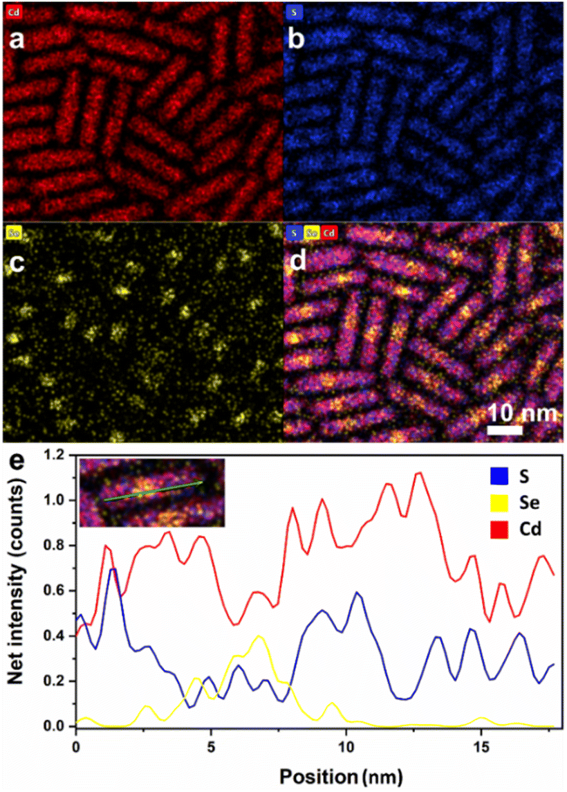 | ||
| Fig. 4 Representative TEM EDS mapping of one of the many samples, DR15, with a length of 18.3 ± 2.8 nm and a diameter of 3.8 ± 0.6: |(a–c) representative EDS mapping images for Cd, S, and Se, (d) merging of Cd, S, and Se maps, and (e) line-scan distribution profiles of Cd, S, and S in a DR. | ||
3.2 Variation of the shell thickness of the DRs with reaction temperature
To clarify the discrepancies observed in Fig. 1 over the 593–653 K temperature range, Fig. 5, S2† and Table 3; illustrate and detail the variation in the DRs' length and CdS shell thickness when controlling the temperature inside the reactor and varying this temperature over a wide range (503–653 K), including those in Fig. 1. | ||
| Fig. 5 Variation of the cylindrical length, l = L − D, and the shell thickness, S = (D − Ds)/2, with the injected thermal energy after an 8-minute reaction time; the corresponding injection temperatures are indicated on the top axis. During the 8-min reaction time, the 1D-growth regime is preserved up to 593 K. Beyond this temperature, the growth shifts toward the 3D-growth regime; eventually, DR reshaping also occurs within the 8-min reaction time necessary for the reaction temperature to reach 623 K. CdSe seeds (3.2 nm) at a concentration of 18.8 μM and T = 593 K; see text for the data fitting. | ||
| Name | T Injection (K) | Length L (nm) | Diameter D (nm) | AR l/D | (D − Ds)/2 (nm) | VolumeaV (nm3) |
|---|---|---|---|---|---|---|
| a Overall volumeV = πD2(L − D/3)/4, assuming a cylindrical shape with two hemispherical ends. | ||||||
| DR-7 | 503 | 6.2 ± 0.7 | 3.6 ± 0.4 | 1.7 | 0.2 | 50.9 |
| DR-8 | 533 | 8.3 ± 0.8 | 3.7 ± 0.5 | 2.2 | 0.25 | 76.0 |
| DR-9 | 563 | 12.0 ± 1.0 | 3.8 ± 0.4 | 3.2 | 0.3 | 121.7 |
| DR-10 | 593 | 24.3 ± 1.6 | 3.8 ± 0.4 | 6.4 | 0.3 | 261.2 |
| DR-11 | 623 | 32.5 ± 2.0 | 4.9 ± 0.5 | 6.6 | 0.85 | 582.1 |
| DR-12 | 653 | 30.4 ± 2.5 | 5.8 ± 0.8 | 5.2 | 1.3 | 752.1 |
Fig. 5 shows that 1D-growth is preserved for at least 8 min, provided the injection temperature remains below 593 K. The shell thickness can, thus, remain very thin while the overall length L of the DRs, and consequently the overall aspect ratio L/D, can be tuned up to 6.4 under present experimental conditions.
Moreover, using the data from Table 3, and the linearity between (V1d − Vseed) and l1d in the 1D-growth regime ((V1d − Vseed)(t) ≈ πl1d(t)D021d/4), we find πD021d/4 = (12.07 ± 0.20) nm2 from which we can deduce a statistical average final diameter of D01d = (3.92 ± 0.03) nm. This value, now obtained from experiments conducted at different temperatures after an 8-minute reaction time, strengthens the fact that just a single CdS monolayer (0.35 nm) grows on the CdSe seeds (Ds = 3.2 nm) during the first growth stage, regardless of the reaction temperature.
Also, temperature investigations give access to activation energies necessary for DR growth. On the one hand, let τ1,3 denote the crossover time at which the growth switches from 1D to 3D. Then, the axial growth rate dl/dt ≅ 4VMks[C]∞ continues to predict l3d(t) ≅ 4VMks[C]∞t. Moreover, as l/D ≫ 1 at τ1,3 in Fig. 5, the radial growth rate dD/dt ≈ 2VMl/l + Dkc[C]∞ ≈ 2VMkc[C]∞ leads to D3d(t) ≈ D01d + 2VMkc[C]∞(t − τ1,3). We deduce the CdS shell thickness variation, S3d(t > τ1,3) = (D3d − D01d)/2 ≈ VMkc[C]∞(t − τ1,3). On the other hand, the DR growth reaction rate constants, ks,c, of the solute are known to follow Arrhenius' laws in temperature of the form ks,c = k0s,c exp(−Es,c/RT), where Es,c represents the growth activation energies at the DR surfaces, at their spherical tips and the cylindrical part, respectively. Consequently, at a given time and for an initial solute concentration of [C]∞, we expect: (i) l1d,3d(T) ∝ ks(T) ∝ exp(−Es/RT) during the 1D- and the 3D-growth stages and, (ii) S3d(T) ∝ kc(T) ∝ exp(−Ec/RT) for the 3D-growth stage. Thus, the temperature-dependent variations in the DR shell thickness and length should allow the determination of the corresponding axial and radial energies of activation (Fig. 5).
The axial growth exponential fitting yields Es ≈ (51 ± 8) kJ mole−1. The determination of Ec from the 3D-radial growth stage is less accurate because it is difficult to obtain much data free from DR reshaping; only an order of magnitude can be given using three shell thickness measurements. The corresponding exponential fitting yields Ec ≈ (70 ± 18) kJ mole−1. Considering the errors resulting from data fitting, Ec ∼ Es, which suggests that the energy cost for radial and axial solute incorporation is not a determinant quantity to explain the difference between 1D- and 3D-growth.
Activation energy data are scarce in the literature for comparison. For instance, Viswanatha et al.57 performed experiments on the growth of CdS nanoparticles in the absence of surface ligands and over a narrow and low-temperature range (333–373 K); they also adjusted their concentrations to maintain the growth of their CdS nanoparticles in the spherically isotropic Ostwald ripening regime. They found an activation energy of Ea ∼ 142 ± 3 kJ mole−1, i.e., typically twice as high as the Es obtained for the 3D-growth at the DR tip with the same spherical symmetry. Nonetheless, both the presence of ligands on the DR surface, which are known to reduce diffusion phenomena, and the higher reaction temperature (503–653 K) level may explain this difference in values. This hypothesis is strengthened by another work on the spherical growth of CdS nanocrystals in a hot paraffin matrix developed by Yordanov et al.68 Working in the spherically isotropic Ostwald ripening regime, they found that the growth rate was slower when using a coordinating matrix (Tri-n-octyl phosphine oxide, (TOPO)) instead of a non-coordinating one (tributylphosphine sulfide (TBP-S) in liquid paraffin). Further analysis using TBP-S gave an activation energy of Ea ∼ 51.9 kJ mole−1 within the temperature range of 473–533 K,69 comparable to our measured value (average value: Es ∼ 60 kJ mole−1).
Consequently, the reaction temperature plays a crucial role in the growth process, and 593 K seems to be an optimized value for achieving the highest aspect ratio before 3D growth and reshaping occur. Finally, this temperature-controlled investigation clarifies the dispersion in results observed in previous studies, many of which were based on reaction temperatures above 623 K.38,41,45,49–51,63
3.3 Variation of the thin-shell DR aspect ratio with the seed concentration
DRs with different aspect ratios have mostly been obtained in the literature by varying the seed diameter,41,48,50,70 reaction time,40,45 ligands,34 or amounts of precursors.16,71–73 We propose an additional parameter in the present work: the concentration [CdSe] of the CdSe seeds in solution (Fig. 6, 7 and Table 4).20,34 | ||
| Fig. 6 TEM images of DRs synthesized starting with different CdSe seed concentrations. (a) DR-15, 36.5 μM, (b) DR-10, 18.8 μM, (c) DR-5, 14 μM, (d) DR-14, 7.3 μM, and (e) DR-13, 3.7 μM, and (f) variation of DR length distributions obtained at different seed concentrations (593 K). | ||
 | ||
| Fig. 7 Linear variation of the volume V − Vs of the DRs versus the length l = L − D of their cylindrical part in the 1D-growth regime, at T = 593 K and after 8 min of reaction, when varying the seed concentration [CdSe]. | ||
| Name | [Seed]a (μM) | Length (nm) | Diam. (nm) | ARb | Shell-thickness (nm) | V (nm3) |
|---|---|---|---|---|---|---|
| a The seed concentration was calculated from the absorption spectrum using Peng's equation (nm).54 b AR = L/D ((L − D)/D). c Overall volume V = πD2(L − D/3)/4, assuming a cylindrical shape with hemispherical ends. | ||||||
| DR-13 | 3.7 | 74.6 ± 7.1 | 3.7 ± 0.5 | 20.2 (19.2) | 0.3 | 788.84 |
| DR-14 | 7.3 | 52.7 ± 3.7 | 3.6 ± 0.4 | 14.6 (13.6) | 0.2 | 524.21 |
| DR-5 | 14 | 38.7 ± 3.5 | 3.6 ± 0.4 | 10.8 (9.8) | 0.2 | 381.7 |
| DR-10 | 18.8 | 24.3 ± 1.6 | 3.8 ± 0.4 | 6.4 (5.4) | 0.3 | 261.24 |
| DR-15 | 36.5 | 18.3 ± 2.8 | 3.8 ± 0.6 | 4.8 (3.8) | 0.3 | 193.17 |
Table 4 shows that the shell-thickness of the DRs remains less than 1 monolayer (one monolayer of CdS having an average thickness of 0.35 nm) as the seed concentration decreases. Meanwhile, their length not only increases (Fig. 6) but also exhibits a much narrower size distribution.
These behaviors can be quantitatively understood by mass conservation at time t. Indeed, the volume of material consumed at time t for DR growth, VM[C(t)] = VM × Min{[Cd](t),[S](t)}, should be equal to the number of seeds per liter, Ns, multiplied by the increase in individual DR volume due to material consumption: Ns(V(t) − Vseed). Then, as  , where
  is the Avogadro number, we deduce (eqn (2)):
 | (2) |
Working in the 1D-growth regime, (V(t) − Vseed) ≈ (V1d − Vseed)(t) ≈ πl1d(t)(D01d)2/4, where D01d = Ds + 2CdS layers (Ds = 3.2 nm plus twice 0.35 nm). Then, at a given reaction time (8 min), temperature (593 K) and cadmium precursor concentration ([Cd] = 0.55 M), we expect from eqn (2): l1d ∝ (V1d − Vseed) ∝ [CdSe]−1, D1d = D01d ∝ [CdSe]0, and  , all linear in [CdSe]−1, except D1d ∼ Ds which is fixed as the initial condition.
Moreover, the diameter D of the DRs remains constant over the investigated range of CdSe seed concentrations, corresponding to almost one order of magnitude variation. Finally, Fig. 7 shows that (V1d − Vseed) is indeed linear in l1d, and the slope of πD021d/4 = (10.75 ± 0.21) nm2, allows deducing a statistical mean diameter of D01d = (3.70 ± 0.04) nm, during 1D-growth. This value corresponds to a seed diameter of Ds = 3.2 nm covered with a single CdS layer (0.35 nm) and gives one more proof of the isotropic growth of a single CdS shell before switching to the 1D-growth regime.
In conclusion, CdSe/CdS DRs with a thin shell close to a single CdS layer can be synthesized with high accuracy and predictability when the reaction temperature is well controlled, including the influence of the initial thermal conditions (see the ESI (Tables S1 and S2)).† This approach was also extended to other CdSe seed sizes (Fig. S3 and S4 and Table S3†). Moreover, their overall aspect ratio can be continuously varied between 1 and 20 (DR13), just by adjusting the reaction time and/or seed concentration at the optimized reaction temperature. Finally, as illustrated in Fig. 3 over time and Fig. 5 with varying temperatures, the 3D-growth process enables variations and adjustments in the shell thickness as needed. Consequently, we had a set of available samples for studying in detail the influence of the envelope and length on the chiroptical properties of these CdSe/CdS nano-objects.
3.4. Influence of the shell thickness on the chirality of DRs
To check how the shell thickness can affect the CD g-factor signal of chiral DRs, we selected a series of DRs with four different shell thicknesses ranging from 0.35 to 2.0 nm (DR-10, DR-11, DR-12, and DR-23 (Table S4†), ARs ranging from 3.5 to 6.6, and lengths about 25–30 nm. The thickest shell (DR-23) was obtained with a method combining an established fast-injection-based step for Cd and S precursors to create the initial shell, followed by a second slow injection growth that allows for systematic variation of the shell thickness while maintaining a high degree of monodispersity at the batch level and uniformity at the single-nanorod level, as reported by Bawendi's group.38 The shell thickness increased to 2.0 nm through two slow-growth steps separated by a purification step (Fig. S5†). The UV-vis and PL spectra of the samples are shown in Fig. S6 and S7.†We chose ligand-induced chirality among the several methods for inducing chirality in QDs.2,3,16,20 Induced chirality in the aqueous phase relies on the replacement of the original achiral ligand with a chiral one on the semiconductor nanoparticles.15,16,29,30,74 Gun'ko and co-workers were the first to report the observation of circular dichroism (CD) response induced in excitonic transitions of CdS quantum dots (QDs) capped with chiral molecules.18 However, the CD g-factor they found was quite low (typically 10−4 or even 10−5).16,75–78 Since, on the one hand, the induced chiral signal intensity of the core–shell systems has been shown to increase with decreasing shell thickness,24 and on the other hand, we have recently observed that CdSe/CdS DRs have great potential for high ligand-induced chirality,16,17 we aim to use our actual control of shell thickness down to ultra-thin shell DRs to generate and study high ligand-induced chiral signals.
To prepare these chiral DRs, we extracted the organic colloidal phase using an aqueous phase with cysteine (Cys) ligands as previously discussed (Fig. 8).16,17
 | ||
| Fig. 8 The ligand exchange process of DRs from the oil phase to the aqueous phase. | ||
To do so, cysteine was dissolved in deionized (DI) water (5 mL, [Cys] = 0.1 M); the pH of the resulting solution was then adjusted to 12.0 with a 25% aqueous solution of tetramethylammonium pentahydrate (TMAH). A solution of CdSe/CdS DRs in n-hexane (5 mL, 1 μM) was added to the aqueous cysteine solution; the reaction mixture was then purged with nitrogen and stirred at room temperature, under an inert atmosphere for 24 h in the absence of light. The reaction mixture was then allowed to rest for 1 h to allow phase separation. The bottom aqueous layer, now containing the DRs, was removed with a syringe, and purified twice by precipitation with ethanol/DI water/chloroform (4:1:1). As an example, purified Cys-DRs were dispersed in deionized H2O and stored at room temperature in the dark. Fig. S8† shows the luminescence of the DRs listed in Table 3; before (a and b) and after (c and d) the ligand exchange and transfer from the organic to the aqueous phase. From left to right, we observe the CdSe QDs, and DRs with different aspect ratios, respectively. The luminescence of the different DRs is well preserved, but that of the pure CdSe is almost completely quenched.
We then focused on the UV-vis and CD studies performed on samples with increasing shell thicknesses with also comparable lengths, listed in pairs in Table S4† and shown in Fig. 9.
 | ||
| Fig. 9 CD spectra and the corresponding UV/vis absorption spectra of the L- and D-Cys-CdSe/CdS DRs with different shell thicknesses. (a) DR-10, (b) DR-11, (c) DR-12, and (d) DR-23. | ||
The results show that the strong CD signal observed for CdSe/CdS DRs with one or two monolayers (DR-10 and DR-11) decreases and is completely suppressed when the shell becomes thicker (DR-12 and DR-23), as expected due to the effect mediated by hole interactions with the surface. This phenomenon is independent of the DR length, as illustrated by the similar lengths of DR-10 and DR-23. The CD g-factor signal decreased by more than 5-fold as the shell thickness increased from 0.35 to 2.10 nm (one to six layers) (Fig. 10, Tables S5 and S6†), as also observed by Purcell-Milton.24
 | ||
| Fig. 10 Variation of the CD g-factor of the DRs with their shell thickness (Table S4†). Green dots: additional data from ref. 16 (Tables S2 and S3†) and blue ones from ref. 34 with identical seed diameter. | ||
This study not only confirms, the behaviour observed by Purcell et al.24,79 in QDs for DRs, i.e., an inverse relationship between the CD g-factor and the number of shell layers (consistent with the increase in the distance between the chiral ligands and the holes localized at the CdSe core level) but also shows that this behaviour (i) takes place in a range of g-values an order of magnitude higher than in QDs, (ii) is linear, and (iii) does not follow an exponential trend.
3.5 Influence of the length of the DRs on their chirality
We also demonstrated that the main consequence, i.e., the decrease in coupling between the seed holes and the chiral source, also depends on the DR length. Indeed, as illustrated in Fig. 11a–e, the symmetrical CD signal intensities of both L- and D-modified surfaces measured at the maximum wavelength (∼475 nm) increase with the aspect ratio of the nanorods (see Table 3 (AR), S7, and S8† (CD anisotropy g CD-factors)), with values ranging from 0.23 × 10⁻³ to 1.3 × 10⁻³ when varying the AR from 4.8 to 14.6. It then remained constant at more than 10−3 as the AR continued to increase (Fig. 11f). To the best of our knowledge, this is the first report on CdSe/CdS DRs with such high-induced chirality (more than 10−3) using a single small molecule. Although Kuang et al.34 reported CD g-factors of 1.2 × 10⁻³, they used a mixture of two different ligands (D-cysteine and D-histidine), whereas each ligand, on its own, induced a CD g-factor of only 0.52 × 10⁻³. | ||
| Fig. 11 Variation of the CD signal with the DR aspect ratio, in the 400–500 nm region of the CdS absorption (CdSe seed size Ds = 3.2 nm). (a–e) CD signal of DR-15, DR-10, DR-5, DR-14, and DR-13, from Table 3; (f) Resulting CD g-factor variation of the same DRs (lines are guides for the eyes). Blue and green data are from ref. 78 for pure CdSe QRs. Lines are also guides for the eyes. | ||
A closer look at Fig. 11 further highlights the significant added value of a thin CdS shell as compared to pure CdSe nanorods.78 The combined effects of the CdSe core and CdS shell generate a chiral signal for the CdSe/CdS DRs that is higher than that of pure CdSe or CdS. As the aspect ratio increases, the CdS shell gradually grows along the [001] axis, which increases the anisotropy and leads to chirality enhancement.
4 Conclusions
In this work, we have shown that DR synthesis is finely driven by a temperature-dependent two-step mechanism. Using CdSe seeds with a regular polyhedral morphology, the first transient stage involves growing a very thin, wurtzite-CdS64 spherical shell with a thickness close to one atomic layer. The second stage is triggered by the emergence of facets with different surface energies on this CdS layer that drive the growth to become anisotropic and promote the DR morphology (so-called 1D-growth by Peng55). The increase in the AR, while maintaining a thin shell, has been optimized by fine-tuning (i) the reaction time (which must be around 8 min), (ii) the reaction temperature (injection and ambient temperature and power of the heating mantle) (which must be around 593 K), and (iii) the seed concentration (close to 10 μM for AR > 10). Playing with all these parameters, we successfully prepared DRs with an ultra-thin shell layer and different ARs up to 20 (Table 3).The reaction temperature plays a crucial role in the growth process, and 593 K appears to be the optimized value for which the highest AR is reached before 3D growth and reshaping take place. Eventually, this study on the control of the temperature elucidates the discrepancies in results observed in the aforementioned studies, where many used reaction temperatures above 623 K.
Under optimal conditions, we could achieve DRs with a thin shell thickness of approximately 0.35 nm, corresponding to a single atomic layer of CdS and ARs ranging from 4.8 to 20. Their CD g-factor values varied from 0.23 × 10⁻³ to 1.30 × 10⁻³. Notably, the CD g-factor value of 1.3 × 10⁻³ represents the highest ligand-induced chirality achieved to date for this type of nanorods by simply controlling their length and shell thickness. Additionally, only one type of chiral ligand was used. This approach gives these structures great potential for further applications in the chirality domain. Most of all, this study provides a platform for the exploration of various dimensions of nanostructures with controllable anisotropy. Finally, we anticipate that this ultra-thin shell adjustment strategy can be extended to other types of seed-grown semiconductor nanoparticles, enhancing their chiral signal and catalytic properties with significant practical implications.
Data availability
The authors confirm that the data supporting the findings of this study are available within the article [and/or its ESI†].Author contributions
The manuscript was written through the contributions of all authors. All authors have approved the final version of the manuscript.Conflicts of interest
There are no conflicts to declare.Acknowledgements
TEM data were obtained using microscopes at the Plateforme Aquitaine de Caractérisation des Matériaux (PLACAMAT, UMS 3626, CNRS, Univ. Of Bordeaux, Pessac, France) and the Southern University of Science and Technology Core Research Facilities. The authors acknowledge the technical support from Marion Gayot at PLACAMAT, as well as Dongsheng He and Yang Qiu at SUSTech CRF (Nouveaux Matériaux 2020 and 2021). The authors acknowledge the funding support from the National Key Research and Development Program of China (No. 2022YFB3602903, 2021YFB3602703, and 2022YFB3606504), the National Natural Science Foundation of China (No. 62204107 and 12204318), the Guangdong Basic and Applied Basic Research Foundation (No. 2022A1515011614 and 2021A1515110535), the Shenzhen Science and Techn. Program (No. JCYJ20220818100411025 and RCYX20221008092908030), the Shenzhen Key Laboratory for Advanced Quantum Dot Displays and Lighting (No. ZDSYS201707281632549), the Pingshan District Innovation Platform Project of Shenzhen Hi-tech Zone Development Special Plan in 2022 (29853M-KCJ-2023-002-01), and the Natural Science Foundation of Top Talent of SZTU (grant no. GDRC202344 and GDRC202340). P. M.-B acknowledges funding from the Deutsche Forschungsgemeinschaft (DFG, German Research Foundation) under Germany's Excellence Strategy – EXC 2089/1 – 390776260. P. L. and W. C. gratefully acknowledge financial support from the Chinese Scholarship Council (CSC). MHD and JPD acknowledge the CNRS through the MITI interdisciplinary programs (Action MITI: Nouveaux Matériaux 2020 and 2021).Notes and references
- A. Ben-Moshe, A. O. Govorov and G. Markovich, Angew. Chem., Int. Ed., 2013, 52, 1275–1279 CrossRef CAS PubMed.
- J. Yeom, B. Yeom, H. Chan, K. W. Smith, S. Dominguez-Medina, J. H. Bahng, G. Zhao, W.-S. Chang, S.-J. Chang, A. Chuvilin, D. Melnikau, A. L. Rogach, P. Zhang, S. Link, P. Král and N. A. Kotov, Nat. Mater., 2014, 14, 66 CrossRef PubMed.
- M. V. Mukhina, V. G. Maslov, A. V. Baranov, A. V. Fedorov, A. O. Orlova, F. Purcell-Milton, J. Govan and Y. K. Gun’ko, Nano Lett., 2015, 15, 2844–2851 CrossRef CAS PubMed.
- A. Kühnle, T. R. Linderoth, B. Hammer and F. Besenbacher, Nature, 2002, 415, 891–893 CrossRef PubMed.
- A. Ben-Moshe, A. Teitelboim, D. Oron and G. Markovich, Nano Lett., 2016, 16, 7467–7473 CrossRef CAS PubMed.
- G. Yang and H. Zhong, Isr. J. Chem., 2019, 59, 639–648 CrossRef CAS.
- S. Huo, P. Duan, T. Jiao, Q. Peng and M. Liu, Angew. Chem., Int. Ed., 2017, 56, 12174–12178 CrossRef CAS PubMed.
- Y. Xia, Y. Zhou and Z. Tang, Nanoscale, 2011, 3, 1374–1382 RSC.
- M. Sun, L. Xu, A. Qu, P. Zhao, T. Hao, W. Ma, C. Hao, X. Wen, F. M. Colombari, A. F. de Moura, N. A. Kotov, C. Xu and H. Kuang, Nat. Chem., 2018, 10, 821–830 CrossRef CAS PubMed.
- E. Shah and H. P. Soni, RSC Adv., 2013, 3, 17453–17461 RSC.
- L. Xiao, T. An, L. Wang, X. Xu and H. Sun, Nano Today, 2020, 30, 100824 CrossRef CAS.
- W. Ma, L. Xu, A. F. de Moura, X. Wu, H. Kuang, C. Xu and N. A. Kotov, Chem. Rev., 2017, 117, 8041–8093 CrossRef CAS PubMed.
- X. Zhao, S.-Q. Zang and X. Chen, Chem. Soc. Rev., 2020, 49, 2481–2503 RSC.
- X. Liu and R.-H. Jin, Chem. Synth., 2022, 2, 7 CAS.
- U. Tohgha, K. K. Deol, A. G. Porter, S. G. Bartko, J. K. Choi, B. M. Leonard, K. Varga, J. Kubelka, G. Muller and M. Balaz, ACS Nano, 2013, 7, 11094–11102 CrossRef CAS PubMed.
- J. Cheng, J. Hao, H. Liu, J. Li, J. Li, X. Zhu, X. Lin, K. Wang and T. He, ACS Nano, 2018, 12, 5341–5350 CrossRef CAS PubMed.
- J. Hao, Y. Li, J. Miao, R. Liu, J. Li, H. Liu, Q. Wang, H. Liu, M.-H. Delville, T. He, K. Wang, X. Zhu and J. Cheng, ACS Nano, 2020, 14, 10346–10358 CrossRef CAS PubMed.
- M. P. Moloney, Y. K. Gun'ko and J. M. Kelly, Chem. Commun., 2007, 38, 3900–3902 RSC.
- S. D. Elliott, M. P. Moloney and Y. K. Gun'ko, Nano Lett., 2008, 8, 2452–2457 CrossRef CAS PubMed.
- Y. Zhou, M. Yang, K. Sun, Z. Tang and N. A. Kotov, J. Am. Chem. Soc., 2010, 132, 6006–6013 CrossRef CAS PubMed.
- T. Nakashima, Y. Kobayashi and T. Kawai, J. Am. Chem. Soc., 2009, 131, 10342–10343 CrossRef CAS PubMed.
- A. Ben-Moshe, A. O. Govorov and G. Markovich, Angew. Chem., Int. Ed., 2013, 52, 1275–1279 CrossRef CAS PubMed.
- A. S. Baimuratov, I. D. Rukhlenko, Y. K. Gun’ko, A. V. Baranov and A. V. Fedorov, Nano Lett., 2015, 15, 1710–1715 CrossRef CAS PubMed.
- F. Purcell-Milton, A. K. Visheratina, V. A. Kuznetsova, A. Ryan, A. O. Orlova and Y. K. Gun’ko, ACS Nano, 2017, 11, 9207–9214 CrossRef CAS PubMed.
- G. Yang, M. Kazes and D. Oron, Adv. Funct. Mater., 2018, 28, 1802012 CrossRef.
- E. D. Sone, E. R. Zubarev and S. I. Stupp, Angew. Chem., Int. Ed., 2002, 41, 1705–1709 CrossRef CAS.
- Y. Zhou, R. L. Marson, G. van Anders, J. Zhu, G. Ma, P. Ercius, K. Sun, B. Yeom, S. C. Glotzer and N. A. Kotov, ACS Nano, 2016, 10, 3248–3256 CrossRef CAS PubMed.
- W. Feng, J.-Y. Kim, X. Wang, H. A. Calcaterra, Z. Qu, L. Meshi and N. A. Kotov, Sci. Adv., 2017, 3, e1601159 CrossRef PubMed.
- X. Qiu, J. Hao, J. Li, Z. Gong, S. Li, J. Cheng, X. Lin and T. He, Opt. Lett., 2019, 44, 2256–2259 CrossRef CAS PubMed.
- Y. Shi, Z. Zhou, X. Miao, Y. J. Liu, Q. Fan, K. Wang, D. Luo and X. W. Sun, J. Mater. Chem. C, 2020, 8, 1048–1053 RSC.
- J. Hao, F. Zhao, Q. Wang, J. Lin, P. Chen, J. Li, D. Zhang, M. Chen, P. Liu, M.-H. Delville, T. He, J. Cheng and Y. Li, Adv. Opt. Mater., 2021, 9, 2101142 CrossRef CAS.
- J. Hao, J. Li, M. Chen, X. Duan, B. Xu, Y. Li, T. He, X. W. Sun, M.-H. Delville and J. Cheng, Mater. Chem. Front., 2022, 6, 1194–1208 RSC.
- Y. Ben-Shahar and U. Banin, Top. Curr. Chem., 2016, 374, 54 CrossRef PubMed.
- W. Ma, J. Mao, C. Hao, L. Xu, C. Xu and H. Kuang, Appl. Catal., B, 2019, 245, 691–697 CrossRef CAS.
- T. O'Connor, M. S. Panov, A. Mereshchenko, A. N. Tarnovsky, R. Lorek, D. Perera, G. Diederich, S. Lambright, P. Moroz and M. Zamkov, ACS Nano, 2012, 6, 8156–8165 CrossRef PubMed.
- K. Wu, Z. Chen, H. Lv, H. Zhu, C. L. Hill and T. Lian, J. Am. Chem. Soc., 2014, 136, 7708–7716 CrossRef CAS PubMed.
- K. Wu, H. Zhu and T. Lian, Acc. Chem. Res., 2015, 48, 851–859 CrossRef CAS PubMed.
- I. Coropceanu, A. Rossinelli, J. R. Caram, F. S. Freyria and M. G. Bawendi, ACS Nano, 2016, 10, 3295–3301 CrossRef CAS PubMed.
- N. G. Pavlopoulos, J. T. Dubose, Y. Liu, X. Huang, N. Pinna, M.-G. Willinger, T. Lian, K. Char and J. Pyun, CrystEngComm, 2017, 19, 6443–6453 RSC.
- D. Kim, Y. K. Lee, D. Lee, W. D. Kim, W. K. Bae and D. C. Lee, ACS Nano, 2017, 11, 12461–12472 CrossRef CAS PubMed.
- L. Carbone, C. Nobile, M. De Giorgi, F. D. Sala, G. Morello, P. Pompa, M. Hytch, E. Snoeck, A. Fiore, I. R. Franchini, M. Nadasan, A. F. Silvestre, L. Chiodo, S. Kudera, R. Cingolani, R. Krahne and L. Manna, Nano Lett., 2007, 7, 2942–2950 CrossRef CAS PubMed.
- W. Zhang, M. F. Prodanov, J. Schneider, S. K. Gupta, T. Dudka, V. V. Vashchenko, A. L. Rogach and A. K. Srivastava, Adv. Funct. Mater., 2019, 29, 1805094 CrossRef.
- I. Hadar, J. P. Philbin, Y. E. Panfil, S. Neyshtadt, I. Lieberman, H. Eshet, S. Lazar, E. Rabani and U. Banin, Nano Lett., 2017, 17, 2524–2531 CrossRef CAS PubMed.
- A. Polovitsyn, A. H. Khan, I. Angeloni, J. Q. Grim, J. Planelles, J. I. Climente and I. Moreels, ACS Photonics, 2018, 5(11), 4561–4568 CrossRef CAS.
- F. Pisanello, G. Leménager, L. Martiradonna, L. Carbone, S. Vezzoli, P. Desfonds, P. D. Cozzoli, J.-P. Hermier, E. Giacobino, R. Cingolani, M. De Vittorio and A. Bramati, Adv. Mater., 2013, 25, 1974–1980 CrossRef CAS PubMed.
- R. Krahne, M. Zavelani-Rossi, M. G. Lupo, L. Manna and G. Lanzani, Appl. Phys. Lett., 2011, 98, 063105 CrossRef.
- E. Khon, K. Lambright, R. S. Khnayzer, P. Moroz, D. Perera, E. Butaeva, S. Lambright, F. N. Castellano and M. Zamkov, Nano Lett., 2013, 13, 2016–2023 CrossRef CAS PubMed.
- C. She, A. Demortière, E. V. Shevchenko and M. Pelton, J. Phys. Chem. Lett., 2011, 2, 1469–1475 CrossRef CAS.
- G. Menagen, D. Mocatta, A. Salant, I. Popov, D. Dorfs and U. Banin, Chem. Mater., 2008, 20, 6900–6902 CrossRef CAS.
- G. Menagen, J. E. Macdonald, Y. Shemesh, I. Popov and U. Banin, J. Am. Chem. Soc., 2009, 131, 17406–17411 CrossRef CAS PubMed.
- S. Deka, A. Quarta, M. G. Lupo, A. Falqui, S. Boninelli, C. Giannini, G. Morello, M. De Giorgi, G. Lanzani, C. Spinella, R. Cingolani, T. Pellegrino and L. Manna, J. Am. Chem. Soc., 2009, 131, 2948–2958 CrossRef CAS PubMed.
- J. Qin, J. Hao, W. Chen, J. Deng, D. Wang, B. Xu, D. Wu, K. Wang, S. Li and Z. Wen, SID Symp. Dig. Tech. Pap., 2016, 47, 428–431 CrossRef CAS.
- Z. Zhou, K. Wang, Z. Zhang, C. Zhang, H. Liu, Y. Zhang, Z. Wen, S. Li, J. Hao, B. Xu, S. J. Pennycook, K. L. Teo and X. W. Sun, IEEE Photonics J., 2019, 11, 1–11 Search PubMed.
- W. W. Yu, L. Qu, W. Guo and X. Peng, Chem. Mater., 2003, 15, 2854–2860 CrossRef CAS.
- Z. A. Peng and X. Peng, J. Am. Chem. Soc., 2001, 123, 1389–1395 CrossRef CAS.
- J. A. Edgar, A. M. McDonagh and M. B. Cortie, ACS Nano, 2012, 6, 1116–1125 CrossRef CAS PubMed.
- R. Viswanatha, H. Amenitsch, S. Santra, S. Sapra, S. S. Datar, Y. Zhou, S. K. Nayak, S. K. Kumar and D. D. Sarma, J. Phys. Chem. Lett., 2010, 1, 304–308 CrossRef CAS.
- H. Su, J. D. Dixon, A. Y. Wang, J. Low, J. Xu and J. Wang, Nanoscale Res. Lett., 2010, 5, 823 CrossRef CAS PubMed.
- X. Chuang, H. Hongxun, C. Wei and W. Jingkang, J. Cryst. Growth, 2008, 310, 3504–3507 CrossRef.
- C. R. Bullen and P. Mulvaney, Nano Lett., 2004, 4, 2303–2307 CrossRef CAS.
- B. Pan, R. He, F. Gao, D. Cui and Y. Zhang, J. Cryst. Growth, 2006, 286, 318–323 CrossRef CAS.
- X. Chen, J. Wang, R. Pan, S. Roth and S. Förster, J. Phys. Chem. C, 2021, 125, 1087–1095 CrossRef CAS.
- W. Chen, K. Wang, J. Hao, D. Wu, J. Qin, D. Dong, J. Deng, Y. Li, Y. Chen and W. Cao, Nanophotonics, 2016, 5, 565–572 Search PubMed.
- G. Bertoni, V. Grillo, R. Brescia, X. Ke, S. Bals, A. Catellani, H. Li and L. Manna, ACS Nano, 2012, 6, 6453–6461 CrossRef CAS PubMed.
- K. Wu, L. J. Hill, J. Chen, J. R. McBride, N. G. Pavlopolous, N. E. Richey, J. Pyun and T. Lian, ACS Nano, 2015, 9, 4591–4599 CrossRef CAS PubMed.
- B. T. Diroll, N. Gogotsi and C. B. Murray, Chem. Mater., 2016, 28, 3345–3351 CrossRef CAS.
- S. Christodoulou, F. Rajadell, A. Casu, G. Vaccaro, J. Q. Grim, A. Genovese, L. Manna, J. I. Climente, F. Meinardi, G. Rainò, T. Stöferle, R. F. Mahrt, J. Planelles, S. Brovelli and I. Moreels, Nat. Commun., 2015, 6, 7905 CrossRef CAS PubMed.
- G. G. Yordanov, C. D. Dushkin, G. D. Gicheva, B. H. Bochev and E. Adachi, Colloid Polym. Sci., 2005, 284, 229–232 CrossRef CAS.
- G. G. Yordanov, E. Adachi and C. D. Dushkin, Colloids Surf., A, 2006, 289, 118–125 CrossRef CAS.
- J. Cheng, E. H. Hill, Y. Zheng, T. He and Y. Liu, Mater. Chem. Front., 2018, 2, 662–678 RSC.
- S. Deka, A. Falqui, G. Bertoni, C. Sangregorio, G. Poneti, G. Morello, M. D. Giorgi, C. Giannini, R. Cingolani, L. Manna and P. D. Cozzoli, J. Am. Chem. Soc., 2009, 131, 12817–12828 CrossRef CAS PubMed.
- D. V. Talapin, J. H. Nelson, E. V. Shevchenko, S. Aloni, B. Sadtler and A. P. Alivisatos, Nano Lett., 2007, 7, 2951–2959 CrossRef CAS PubMed.
- J. J. Li, Y. A. Wang, W. Guo, J. C. Keay, T. D. Mishima, M. B. Johnson and X. Peng, J. Am. Chem. Soc., 2003, 125, 12567–12575 CrossRef CAS PubMed.
- X. Wang, J. Hao, J. Cheng, J. Li, J. Miao, R. Li, Y. Li, J. Li, Y. Liu, X. Zhu, Y. Liu, X. W. Sun, Z. Tang, M.-H. Delville, T. He and R. Chen, Nanoscale, 2019, 11, 9327–9334 RSC.
- J. K. Choi, B. E. Haynie, U. Tohgha, L. Pap, K. W. Elliott, B. M. Leonard, S. V. Dzyuba, K. Varga, J. Kubelka and M. Balaz, ACS Nano, 2016, 10, 3809–3815 CrossRef CAS PubMed.
- M. Puri and V. E. Ferry, ACS Nano, 2017, 11, 12240–12246 CrossRef CAS PubMed.
- I. V. Martynenko, A. S. Baimuratov, V. A. Osipova, V. A. Kuznetsova, F. Purcell-Milton, I. D. Rukhlenko, A. V. Fedorov, Y. K. Gun’ko, U. Resch-Genger and A. V. Baranov, Chem. Mater., 2018, 30, 465–471 CrossRef CAS.
- X. Gao, X. Zhang, K. Deng, B. Han, L. Zhao, M. Wu, L. Shi, J. Lv and Z. Tang, J. Am. Chem. Soc., 2017, 139, 8734–8739 CrossRef CAS PubMed.
- V. Kuznetsova, Y. Gromova, M. Martinez-Carmona, F. Purcell-Milton, E. Ushakova, S. Cherevkov, V. Maslov and Y. K. Gun’ko, Nanophotonics, 2021, 10, 797–824 CrossRef CAS.
Footnotes |
| † Electronic supplementary information (ESI) available: Fig. S1. (a) UV-vis absorption spectra and (b) PL emission spectra of WZ-CdSe cores (λabs = 557 nm). Fig. S2. TEM images of DRs synthesized at different temperatures using the same CdSe cores. Table S1. Physical properties of CdSe/CdS DRs at different reaction times, with two heating power systems. Working temperature 593 K. Table S2. Physical properties of CdSe/CdS DRs at different ambient temperatures (CdSe core 3.2 nm). Table S3. Characterizations of the thin shell CdSe/CdS DRs using different sizes of CdSe cores. Fig. S3. UV-vis absorption and PL emission spectra of CdSe cores with different sizes. Fig. S4. UV-vis absorption and PL emission spectra of CdSe/CdS DRs with thin shell multi-colour. (a) DR-16 (green), (b) DR-15 (orange), (c) DR-17 (red), (d) DR-18 (red). Table S4. Physical properties of CdSe/CdS with different shell thicknesses (CdSe core (3.2 nm). Fig. S5. TEM image of DR-23 with a second over-coating process, the shell thickness is 2.0 nm. Fig. S6. UV-vis absorption and PL emission spectra of CdSe/CdS DRs with different shell thicknesses. Fig. S7. Variation of PL emission spectra of CdSe/CdS DRs with different shell thicknesses. Fig. S8. Images comparing the luminescence before and after the ligand exchange. (a) and (b) the oil phase QDs and DRs in hexane; (c) and (d) the aqueous phase QDs and DRs. Images (a) and (c), under natural light, and (b) and (d) under UV light (365 nm). From left to right: CdSe QDs, and DRs with different aspect ratios (see Table 3 for details). Table S5. The CD anisotropy factors of D-CdSe/CdS DRs with different shell thicknesses (CdSe cores (D = 3.2 nm)). Table S6. CD anisotropy factors of L-CdSe/CdS DRs with different shell thicknesses (CdSe cores (D = 3.2 nm)). Table S7. CD anisotropy factors of D-CdSe/CdS DRs at different core concentrations (CdSe cores (D = 3.2 nm)). Table S8. CD anisotropy factors of L-CdSe/CdS DRs at different core concentrations (CdSe cores (D = 3.2 nm)). See DOI: https://doi.org/10.1039/d4na01003e |
| ‡ These authors contributed equally. |
| This journal is © The Royal Society of Chemistry 2025 |