
 Open Access Article
 This Open Access Article is licensed under a Creative Commons Attribution-Non Commercial 3.0 Unported Licence
Towards enhanced transparent conductive nanocomposites based on metallic nanowire networks coated with metal oxides: a brief review
Abderrahime Sekkat
 *ab,
Camilo Sanchez-Velasqueza,
Laetitia Bardeta,
Matthieu Webera,
Carmen Jiméneza,
Daniel Bellet
a,
David Muñoz-Rojas*a and
Viet Huong Nguyen
*c
*ab,
Camilo Sanchez-Velasqueza,
Laetitia Bardeta,
Matthieu Webera,
Carmen Jiméneza,
Daniel Bellet
a,
David Muñoz-Rojas*a and
Viet Huong Nguyen
*c
aUniv. Grenoble Alpes, CNRS, Grenoble INP, LMGP, 38000 Grenoble, France. E-mail: abderrahime.sekkat@toulouse-inp.fr; david.munoz-rojas@grenoble-inp.fr
bLaboratoire de Génie Chimique, Université de Toulouse, CNRS, INPT, Toulouse, 31432, France
cFaculty of Materials Science and Engineering, Phenikaa University, Hanoi, 12116, Vietnam
First published on 10th September 2024
Abstract
Metallic nanowire networks (MNNs) are promising emerging transparent electrodes (TEs) in multiple application fields. In the last few years, they have been widely reported in the literature as they present attractive physical properties (both electrical and optical) while reducing the amount of required material with respect to conventional TEs, which makes them highly competitive in terms of cost, flexibility, and integrability. Despite all their virtues, MNNs have shown several drawbacks such as rapid degradation and limited capacity for fine-tuning the properties for each specific application. To overcome these issues, several coatings have been thoroughly studied, from polymers, carbonaceous materials, and oxynitrides, to metal oxides. Among these, metal oxides have been largely studied due to their large panoply of properties and different possible synthetic approaches. In this minireview, we provide an overview of the research on metal oxide-coated MNNs, with a particular focus on silver nanowire (AgNW) networks, as they are the most extensively studied. However, the discussion and conclusions drawn here can be directly applied to other metallic nanowires as well. Most importantly, we evaluate the impact of the coating on the fundamental properties and stability of these promising nanocomposites. Finally, a comprehensive overview of various applications based on these specific nanocomposites is presented, including photovoltaics, transparent heaters, smart windows, sensors, diodes, plasmonics, microelectronics, among others. This work offers insights into the potential applications of AgNW-metal oxide nanocomposites in the future and outlines the critical parameters of metal oxide coatings and their functionalities. This work will serve as a guideline towards designing more efficient metal oxide-MNNs through processes compatible with roll-to-roll mass manufacturing for industrial use.
 Abderrahime Sekkat and David Muñoz-Rojas | Abderrahime Sekkat (left in the picture) is an Associate Professor at the National Polytechnic Institute of Toulouse, conducting research at the Chemical Engineering Research Centre (LGC) and a visiting researcher fellow at Inorganic Chemistry Laboratory, University of Oxford. His work focuses on developing functional materials for energy-efficient technologies as well as optoelectronic and electronic applications. He completed his PhD at Grenoble Alpes University (UGA-France), followed by a postdoctoral fellow in the Laboratory of Materials Science and Physical Engineering (LMGP, Grenoble, France). David Muñoz-Rojas (right in the picture) obtained his degree in Organic Chemistry at the Instituto Químico de Sarrià (Barcelona, 1999) and his PhD in Materials Science (2004) at the Instituto de Ciencia de Materiales de Barcelona. Thereafter, he worked as a postdoc at the Laboratoire de Réactivité et Chimie des Solides, the Research Centre for Nanoscience and Nanotechnology, and at the University of Cambridge. He is currently a CNRS researcher at Laboratoire des Matériaux et du Génie Physique in Grenoble. His research focuses on developing cheap and scalable chemical approaches for novel functional materials for electronic and optoelectronic applications. |
 Daniel Bellet | Daniel Bellet is a physicist and has worked in different fields such as single-crystal superalloys, porous silicon, liquid metal embrittlement, sintering of metallic powders, and synchrotron microtomography. His main research now concerns transparent conductive materials. He has been a full professor at Grenoble Institute of Technology since 1998. He was a junior member at IUF from 1999 to 2004 and director of the Academic Research Community “Energies” between 2011 and 2017. He is now the academic scientific director of the Carnot of Future Energies. |
 Viet Huong Nguyen | Viet Huong Nguyen obtained a PhD in Materials Science & Engineering from University Grenoble Alpes, France in 2018. Then, he worked as a postdoctoral fellow in the Laboratory of Materials Science and Physical Engineering (LMGP, Grenoble, France). Since August 2019, he is an assistant professor at Faculty of Materials Science and Engineering, Phenikaa University and is now the Vice Dean of the faculty. His current research interests include the synthesis and surface engineering of nanostructured materials using Atomic Layer Deposition for applications in flexible electronics, gas sensors, and energy conversion & storage. |
1 Introduction and main features of metallic nanowire networks
Transparent electrodes (TEs) are currently a technologically highly relevant type of material since they are key components in many functional devices, such as solar cells, transparent heaters, sensors, light emitting diodes (LEDs) and touch screens, among others.1–4 The most used TE to date is the transparent conductive oxide (TCO) indium tin oxide (ITO). However, ITO faces some challenges due to the scarcity and high cost of indium and because it is usually deposited by sputtering (i.e., an ultrahigh vacuum method, and thus less appealing for scaling up and mass production). In addition, as a ceramic material, it cannot be implemented in emerging applications where flexibility is essential, such as flexible solar cells or flexible electronics.5,6 This has motivated an extensive research into alternative TEs.Numerous materials have thus been investigated as alternative to ITO. These include In-free TCOs,7 such as aluminium-doped zinc oxide (AZO),8 and fluorine-doped tin oxide (FTO),9 as well as organic semiconductors such as poly(3,4-ethylenedioxythiophene) PEDOT films.10–12 While AZO and FTO show comparable properties to ITO, AZO lacks stability and TCOs are generally unsuitable for flexible applications. Furthermore, solution-based organic TEs also impede effective integration into devices due to anisotropic charge injection, hygroscopicity, and acidity, which eventually limit operational stability.13 Further, materials based on carbon nanotubes (CNTs) and MXenes act as potential electrodes in several applications, nevertheless, they suffer from a lack of transparency.14,15
Another alternative TE that has received much attention in this last decade is metallic nanowire networks (MNNs). These materials consist of randomly oriented wires with empty spaces between them, which can be easily deposited at low temperature and thus on any type of substrate. The percolative nature of a metallic nanowire network allows for charge conduction while maintaining optical transparency through the gaps within the network.16 Due to their unique nature, MNNs exhibit several advantages: they require less raw material as compared to traditional TE such as ITO, resulting in lower cost; they present high electrical conductivity and optical transmittance, and excellent mechanical properties.17–20 Silver has been the most commonly studied MNNs, followed in a much lesser manner by copper nanowires due to their lower stability and a more difficult synthesis.21,22 Consequently, this review will exclusively focus on silver nanowire (AgNW) networks. The other metals generally follow a similar design approach, necessitating careful consideration regarding their stability when coated with metal oxides, ensuring stability under growth conditions. Various methods have been employed to synthesize silver nanowires, including electrochemical synthesis, template-assisted synthesis, polyol methods, and UV microwave techniques.23 As shown in Fig. 1a, the polyol process involves the reduction of Ag+ metal ions to form AgNPs (nanoparticles) in the presence of polyvinylpyrrolidone (PVP), which acts as a capping layer, enabling the anisotropic growth yielding metallic nanowires.28,37,38 The AgNW networks thus obtained are made of twins parallel to the nanowire yielding a pentagonal cross-section. The final solution, purified mainly through decantation following purification steps, is used to disperse nanowires onto different substrates.4,39 Once the silver nanowires are prepared, they can be deposited on various type of substrates using different deposition techniques, as described in Fig. 1a, including spin-coating, spray coating, inkjet printing, and Mayer rod coating.24–27 As shown in Fig. 1b, AgNW networks can present state-of-the-art optical and electronic properties, with >95% optical transmittance and 10–30 Ω sq−1 sheet resistance.29 These characteristics may vary depending on the chemical nature of AgNWs and their dimensions and areal mass density (amd), which corresponds to the mass of Ag per unit area. This has also been compared to other potential TEs by assessing Haacke's figure of merit (FoM), specifically Tr10/Rsh, where Tr represents the optical transmittance and Rsh is the sheet resistance. This demonstrates a benchmark of the main advantages of employing AgNW networks as a promising candidate for TE applications, as they depict high transparency and low sheet resistance with respect to poly(3,4ethylene dioxy thiophene):poly(styrenesulfonate) PEDOT:PSS, oxide/Ag/oxide, CNTs, and graphene.16 For further details, several reviews have highlighted the specific characteristics of AgNW networks compared to other TEs across various applications.18,20,40–42 As opposed to ITO and FTO thin films, which undergo significant mechanical degradation (Fig. 1b), high mechanical flexibility of AgNW networks has been also demonstrated in several reports, as almost no change is observed when applying bending with different radius of curvature.28–30
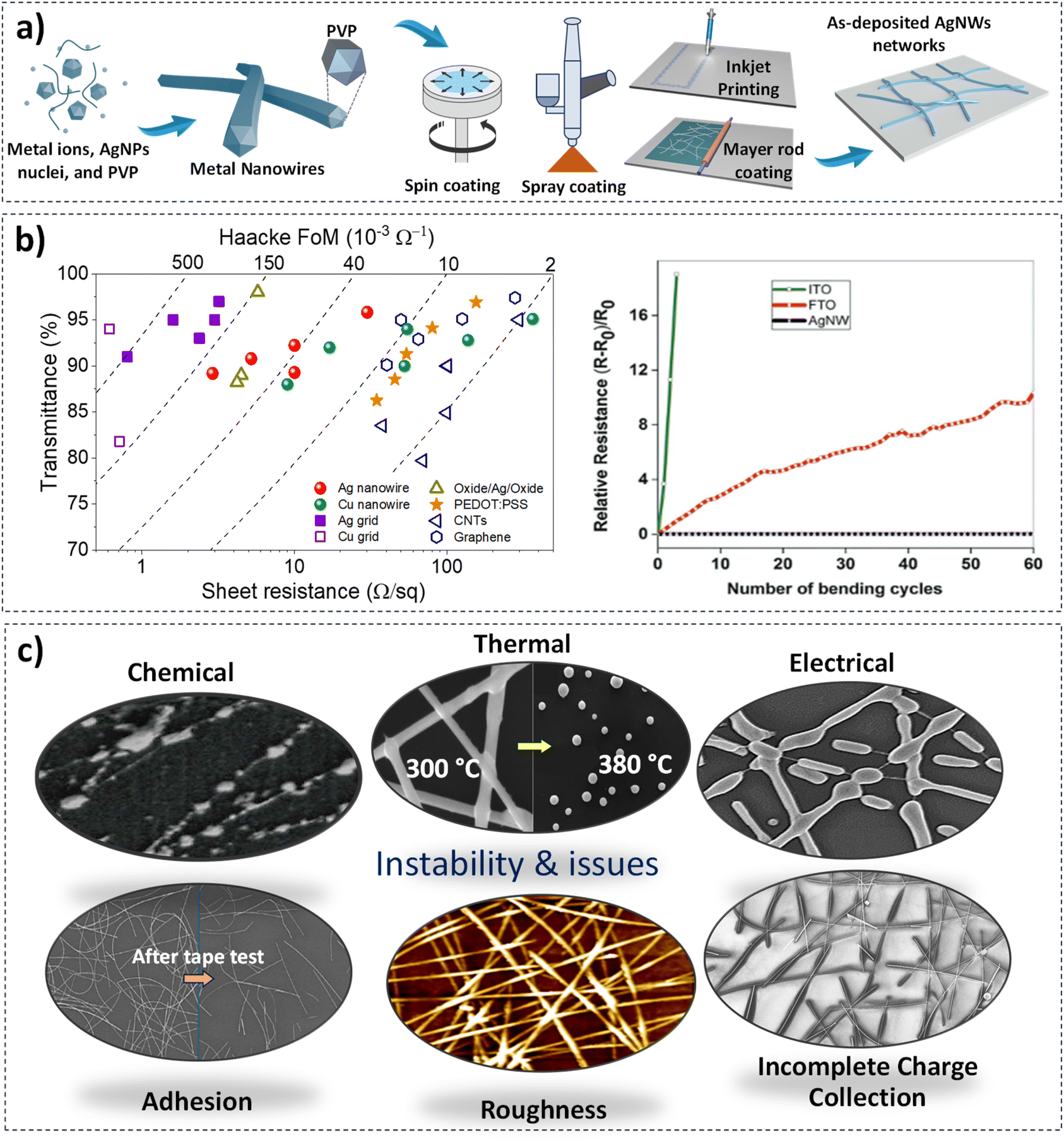 | ||
| Fig. 1 Main features related to Ag nanowire: from synthesis to prevailing properties. (a) Schematic illustration of AgNW network fabrication based on the polyol process and the different ways of fabricating metal nanowire networks including spin-coating,24 spray-coating,25 inkjet printing,26 and Mayer rod coating.27 Main properties of AgNW networks include: (b) electrical and optical properties,28,29 and mechanical properties,4,29,30 (c) morphological stability after thermal,17,31 electrical,32 and chemical stress,33 insufficient charge collection,34 surface roughness,35 and adhesion.36 Reproduced with permission from John Wiley and Sons and Royal Society of Chemistry.4,17 | ||
Nevertheless, the main limitation and issues of AgNW networks lie in their low thermal,17,43 electrical,44 and chemical stability.33,45 Furthermore, they exhibit relatively weak adhesion with rather low roughness, characterized by Root Mean Square (RMS) values ranging from 10 nm to 20 nm (Fig. 1c). Another limitation is associated with the wire–wire resistance at the junctions, which can be improved through various approaches (Fig. 1c).27,35,36 A protective layer is generally necessary as the AgNW networks degrade under harsh conditions (thermal, electrical, and/or chemical stress) with poor adhesion in some cases (Fig. 1c).31,32,46 The proposed coatings would not only enhance the stability of the AgNW networks, but can also serve the purpose of further tuning the properties of the resulting composite TE for specific applications, e.g., adjusting the work function and band alignment, among others. While the coatings are also expected to improve adhesion and homogeneity of the resulting TE, they should not be detrimental to the electrode FoM (i.e., by reducing transparency and/or conductivity). Finally, the coatings should be deposited at low enough temperatures to prevent degradation of the silver nanowires, and ideally ensuring coating conformality (complete coating around the NWs). A recent review has given a general overview of the use of protective layers to enhance the stability of MNN, including the overall coverage, coating of individual NWs (core–shell), and junction-enhancement coatings.47 Others have focused on the challenges and prospects of using MNN in next-generation photovoltaic and sensing applications, while using different architectures.48,49 Our aim in this work, however, is to offer a guideline in selecting the appropriate metal oxide coatings and optimizing their characteristics to achieve optimal performance in specific applications. While we do provide a brief comparison of other coating materials later in this mini-review, our primary focus is on metal oxide coatings. This is because they offer a wide spectrum of benefits, particularly in overcoming the stability limitations of the AgNW networks, while allowing fine-tuning of their properties. Indeed, metal oxides can provide a broad range of characteristic moving from high conductive to dielectric films, having an adjustable optical transmittance (from transparent to semi-transparent) depending on the specific range of light needed. This is the case of tungsten trioxide (WO3), which, when combined with a transparent conductive material (TCM), allows for fine-tuning of optical transmittance of the resulting electrode. This enables the WO3/TCM nanocomposite to be integrated into electrochromic systems with a high optical modulation, making it suitable for smart window applications.50 Most importantly, metal oxides are synthesized with a wide panel of methods from physical to chemical processes ensuring a low-cost, scalable, and flexible manufacturing processes compatible with roll-to-roll industries.
This review provides an analysis of existing strategies for coating percolating metallic nanowires with thin layers of metal oxide to mitigate deterioration as well as to optimize their properties. The various metal oxide types are then categorized based on their suitability for different applications, such as photovoltaic (PV), transparent heaters (TH), sensors, LEDs, among others, highlighting their benefits in each case. Our aim is to provide a guideline to the AgNW networks community in efficiently selecting suitable metal oxides aligned with specific processes for targeted application and performance. Additionally, the main research directions envisaged for the future are also proposed.
2 Main features of AgNW networks coated with metal oxides
As mentioned in the previous section, AgNW networks are emerging structures to form highly efficient TEs with great potential for future development. Nevertheless, they also present some drawbacks related to degradation and operating performance that can be overcome by encapsulation, thus preventing their deterioration over time while improving the mechanical, optical, and electrical properties of the network (flexibility, absorbance, and conductivity). In Section 2.1, the different methods used to grow metal oxides will be discussed with emphasis on the main characteristics of metal oxides-coated AgNW networks. In Section 2.2, the main specifications of metal oxides used for coating AgNW networks will be discussed. Finally, a brief introduction of the different materials used for this purpose will be provided.2.1. Methods to deposit metal oxide thin films
Metal oxide thin films thickness is generally comprised between a few nanometers to one micrometer. In order to coat a AgNW network, a large variety of methods, both physical and chemical, have been explored. These methods lead to different growth mechanisms and properties of the coatings, resulting in different composite electrodes. Therefore, this section will provide a summary of the specifications and features of the different deposition methods allowing to obtain metal oxide thin films. Physical vapor deposition techniques include sputtering (Sputt), pulsed laser deposition (PLD) and evaporation (Evap) processes, whereas chemical processes can be divided in chemical vapor-based routes, electro -chemical/-deposition routes and sol–gel based depositions. Combinations of both approaches (i.e., hybrid processes) such as spin-, spray-, dip-coating, dispersion, and doctor blade coating have been also used. These different types of processes are presented in Fig. 2. | ||
| Fig. 2 The main methods for the deposition of metal oxide thin films coating including chemical, physical, and hybrid processes and their specifications in terms of coating uniformity, deposition rate, conformality, and metal oxides coating metal nanowire networks that are implemented in different type of applications (sputtering,24,51–70 electrospinning,71 electrodeposition/electrochemistry,72–75 pulsed laser deposition (PLD),76 chemical vapor deposition (CVD),77 atomic layer deposition (ALD) and spatial atomic layer deposition (SALD),3,25,78–87 sol–gel/hydrothermal,88–105 spin-coating,106–130 spray-coating/dispersion,131–133 and dip-coating/doctor blade coating.124,134–136). Green, yellow, and red markers correspond to high, moderate, and low levels respectively. | ||
2.1.1.1 Sputtering. In a high vacuum (10−7 bar pressure), an electrical voltage is applied between two electrodes, generating the ionization of the atmosphere (usually argon) and the creation of a plasma discharge.137 The ions present are then accelerated to the cathode (the “target”, i.e., source of the metallic atoms to be deposited). The kinetic energy of the ions is transferred to the atoms of the target that will be ejected, and the gaseous material then deposits onto the substrate (at the opposite side of the reactor) and forms the desired layer having an approximate growth rate varying from 0.1 to 5 nm min−1, resulting in high film uniformity and rather low conformality.138 Different reactive gases can be employed to alter the material composition and stoichiometry.
2.1.1.2 Evaporation. When carrying out a deposition using Evap, the evaporated material is heated until it evaporates at a suitable evaporation rate onto the substrate surface. There are three “sub-processes” that can be defined depending on the evaporation route (inductive, resistance, or electron beam evaporator).138,139 As for Sputt, a high vacuum is required. The layers show a similar structure than sputtering coatings with a deposition rate varying relatively from 5 to 60 nm min−1.
2.1.1.3 Pulsed layer deposition. In the case of PLD, a high-power laser is focused on a specific target, generating particles that condense on the substrate and facilitate the growth of the desired material.140 As for Sputt, different reactive gases are employed to adjust composition and stoichiometry.141 This process provides coating with fair conformality in some cases and low uniformity along with a growth rate varying approximately from 1 to 300 nm min−1, depending on several parameters used during the deposition process.141 Again, high vacuum is needed, from (10−9 to 10−12 bar).137
2.1.2.1 Chemical vapor deposition (CVD). CVD is a powerful chemical route involving the injection of precursor gases into a chamber containing the (heated) substrate to be coated. The deposition temperature is rather high (typically ≥ 400 °C), as the chemical reactions resulting in the desired thin films need to be activated, and the by-products of the reaction along with unreacted precursor gases are exhausted out of the chamber.142 There are many variants of CVD, depending on the particular processing parameters such as the type of precursors, the pressure and the type of activation (thermal, plasma, light).143,144
2.1.2.2 Atomic layer deposition (ALD). ALD is a subclass of CVD, based on the sequential use of self-limiting chemical reactions taking place in a cycle-wise fashion, using successive pulses of precursor and reactant gases separated by purge steps.145,146
This route is widely acknowledged as a powerful deposition technique, enabling the preparation of high quality ultrathin films with a sub-nanometer thickness control, a unique capability among thin film deposition techniques, and at lower substrate temperatures compared with CVD (RT to 400 °C).145,147,148 Spatial ALD (SALD) has been recently developed to achieve higher throughput processing than conventional ALD.149–152 In SALD, the precursors are separated spatially instead of temporally, resulting in SALD growth rates orders of magnitude faster than conventional ALD. Therefore, this route is highly attractive for many industrial applications.3,151,153–156 Both methods allow for coatings with high uniformity, with ALD/SALD processes offering high conformality. However, it is important to note that the deposition rate in ALD (0.1 to 1 nm min−1) is relatively lower when compared to CVD (1 to 100 nm min−1) and SALD (1 to 50 nm min−1) methods.
2.1.2.3 Solution methods. In addition to the deposition routes from the gas phase, depositions can also take place from the liquid phase, the main techniques being electrochemistry or sol–gel processes. Electrochemical based processes, such as electroplating, permit to deposit electrically conductive layers, such as metals, on a given conductive substrate. The basic principle of the route is that the substrate is placed in an electrolytic bath and subjected to an electrical voltage, resulting in the displacement and the deposition of the dissolved metal ions to the cathode (the substrate to be coated with a good uniformity and conformality).157 Finally, chemical bath deposition, based on salts precipitation,158 or sol–gel based processes159 can also be used to prepare thin coatings that are rather uniform but less conformal. Using this latter route, inorganic and hybrid polymer layers can be synthesized from colloidal dispersed solutions by wet-chemical coating processes followed by a curing step. Both processes exhibit approximately low deposition rates in the range of 0.1 to 10 nm min−1.
A summary of various metal oxide-coated AgNW networks used for specific applications is depicted in Fig. 2, demonstrating the different growth methods employed for this purpose. Overall, all the depicted routes present numerous advantages and drawbacks, depending on the applications aimed. In order to coat metallic nanowire networks, an excellent conformality of the deposits and a control of the layer thickness are both required. Therefore, the unique capabilities of ALD make this technique among the most appropriate for this purpose.147,163 And in particular, the spatial ALD (SALD) variant appears to offer additional advantages in terms of deposition rate,152,164 and without the use of vacuum. However, the number of (metal oxide) materials achieved by SALD is still lower than for ALD and/or CVD.
2.2. Main specifications of (Metal Oxides) MOx used for coating AgNW networks
When considering the coating of AgNW networks, several criteria are very important to discuss, including the film homogeneity, the surface coverage, and morphology. In particular, the conformality of the coating will vary depending on the method used. In the case of ALD, which relies on self-limiting reactions and sequential injection, it enables the achievement of conformal growth over complex substrates such as AgNW networks, as shown in Fig. 3a. | ||
| Fig. 3 Main features related to the coating of metallic nanowires depending on the coating process. Metal oxides (MOx) homogeneity, surface coverage, and conformality on the silver nanowires depending on the method employed, namely (Ch.) chemical processes (a) ALD, (b) CVD, and (Phys.) physical processes (c) Sputt, Evap, and PLD. | ||
This is particularly advantageous for applications requiring full surface coverage to avoid any defects that could deteriorate the device performance. Nevertheless, the full and homogeneous coverage is less important and may not be relevant in certain cases, as shown in Fig. 3b, where CVD processes are employed. This is evident in plasmonic based devices, where homogenous coverage is unnecessary to induce adjustable charge transfer processes.104 Physical vapour processes, on the other hand, tend to offer incomplete coverage of the AgNW surface, which can be detrimental for many applications (Fig. 3c). Yet, Fig. 3 provides a scheme of coating morphology obtained from each approach, which may vary slightly depending on the specific nature of the MOx deposited, the deposition method used, and the conditions employed.
As a result, AgNW networks have mostly been coated using chemical and hybrid approaches (which are as well the more attractive for scaling up and mass production). For example, Y. Huang et al. used spin coating to deposit titanium oxide (TiO2) on AgNW networks (Fig. 4a and b).165 The composites showed a smooth surface with low roughness (∼1.9 nm). This surface quality resulted in an improved interfacial adhesion of the wires to the substrate. Furthermore, it enables a conformal deposition of the upper layer for device stacking purposes. On the same line, Khan et al. demonstrated an improved adhesion and high conformality using zinc oxide (ZnO) deposited by SALD, as shown in Fig. 4c and d.166
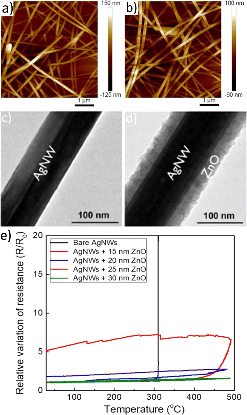 | ||
| Fig. 4 Influence of metal oxide coating on metallic nanowires in terms of roughness and stability. AFM image of (a) AgNW network deposited on a glass substrate, (b) spin-coated TiO2 films on top of AgNW network. TEM images of (c) bare pristine AgNW, (d) AgNW coated with a 30 nm thick ZnO, deposited by SALD. Normalized resistance (e) during thermal stress of bare AgNW network and coated with different ZnO thickness. Reproduced with permission from American Chemical Society.165,166 | ||
In fact, depending on the metal oxide deposited and the growth technique, the resulting oxide coatings present a completely different morphology in terms of crystallinity and roughness. For instance, when MOx is deposited at a lower deposition temperature, it often results in lower film crystallinity and, in some cases, in amorphous films. This is observed in TiO2 or tin oxide (SnO2) deposited by SALD, for instance.25,167 The absence of grain boundaries within amorphous layers leads to lower diffusion coefficients and higher mechanical flexibility.18 Another important aspect is the impact of the intrinsic physical properties of the coating, as some metal oxides such as AZO168,169 and indium oxide (In2O3),170,171 are transparent, while others are designed to enhance the nanocomposites absorption.64,172 Furthermore, the degradation of the nanocomposite highly depends on the film thickness, as demonstrated in the cases of coated ZnO under thermal stress, displaying higher stability for thicker coatings, as shown in Fig. 4e.166
All these results highlight the benefits of coating metal nanowires with metal oxides, as this protective layer enhances the thermal stability of the network. AgNW networks display a large panel of properties with the ability to tune them, thanks to the different available metal oxide coatings. A detailed description of the key features of AgNW networks coated by metal oxides has been previously presented by J. Bang., et al.47 and A. Kumar., et al.40 These MOx have in fact a direct impact on the physical properties of the nanocomposite as it can enhance the mechanical and thermal stability of AgNW networks.4 This is summarized in Fig. 5, where an illustration of bare and coated AgNW networks is shown. The schematic presentation shows the degradation of AgNW network after an annealing treatment, while the coated samples depict a stable behaviour over time at higher deposition temperatures (400 °C). The SEM images illustrate the shape of a degradable AgNW network that spheroidized after an annealing treatment, while the coated one remains stable.31 In fact, SEM proves to be an effective characterization method for evaluating the coating's capacity to protect AgNW networks. The origin of such stability enhancement stems from the fact that a metal oxide conformal coating over AgNW network blocks the silver atomic surface diffusion, preventing spheroidization, while the driving force of the morphological instability (AgNW surface energy reduction) remains intact. In fact, metal oxides have mainly been utilized to improve the long-term stability of AgNW networks under multiple stresses such as external thermal/electrical field,166 mechanical strain,173 and ambient conditions,83 revealing outstanding endurance performances with minimal impact on the optical properties. However, augmenting the thickness of metal oxides (e.g., ZnO or SnO2) typically leads to a reduction in the nanocomposite's optical transparency.45,166 Nonetheless, combining distinct metal oxides with different dielectric constants, such as ZnO/aluminum oxide (Al2O3), can mitigate this effect and enhance optical transparency.174 Besides the nature of metal oxides, using different deposition methods will significantly impact on the film morphology and structure, as mentioned earlier. It is also worth noting that while thicker metal oxide coatings have been reported to enhance the thermal and electrical stability for instance for ZnO166 or SnO2,45 however, for other metallic oxide coatings an optimal thickness is observed: this is the case of the magnesium oxide (MgO) coating for instance.81 Above a given coating thickness, delamination can be observed, cancelling out the stability enhancement. The origin of the delamination likely stems for the thermal dilation mismatch between the metal oxide coating and the substrate, as stated by Sekkat et al.81 Thicker coating will then induce too much strain in the coating layer and delamination occurs to release such elastic energy.
 | ||
| Fig. 5 Schematic summarizing the impact of coating metallic nanowire with metal oxide in terms of stability enhancement. Bare AgNW network spheroidize and degrade over a thermal annealing while coated with SnO2 display more stable structure (as depicted in the SEM images, reproduced with permission from L. Bardet et al.).31 | ||
In addition to visible transmittance, electrical conductivity properties and stability, other features could be of interest. For instance, the haze factor, defined as the ratio between diffuse and total (i.e., direct plus diffuse) transmittance, can play a significate role. While it should be kept small (typically lower than 3%) for displays, conversely the larger the haze factors the better for photovoltaic conversion. In fact, metal oxide coatings can influence the haze factor through modifying the film properties and structures.175,176 One of the main parameters that influences the haze factor for MNW networks is the MNW dimensions: small diameters lead to small haze factor.177 Another key parameter, for instance for smart windows applications, concern the low emission value in the infrared (IR) region: a low IR emissivity, ε, will induce less thermal radiative losses. The IR emissivity for MNW networks depend mainly on the network density, and to a lesser extent on the MNW dimensions.84
Beyond these specified requirements, the metal oxides used to coat AgNW networks must meet additional crucial criteria and possess properties that make them suitable for various targeted applications. The choice of MOx is guided by the specific targeted application, as shown in Table 1. Further elaboration on this aspect is provided in the third section, offering an overview of nanocomposite characteristics and their performance when integrated into different types of applications.
| Reported criteria and properties | Targeted applications | Selected MOx candidates |
|---|---|---|
| Low roughness (Rq < 5 nm) | PV and TEs | IZO, ITO, TiO2 |
| Low absorption (3.2–3.45 eV) | PV | TiO2, ZnO, IZO, FZO, ATO, SnO2, Zn2SnO4 |
| High transparency (77–92%)550 nm | PV, THs, TEs, supercapacitors, and UV-LEDs | AZO, ZnO, ITO, FZO, RuO2, IZO, MnOx, GZO, NiO, SnO2, FTO, MgO |
| High thermal and/or environmental stability (81–400 °C) and 80% humidity | PV, THs, photo-sensors, smart-windows, supercapacitors, electrochromic, TEs, microelectronics, and LEDs | ITO, AZO, AlOx, SnO2, MgO, V2O5, NiO, MoO3, ZnO, ATO, RuO2, Cr2O3, BFO, TiO2 |
| High mechanical flexibility | PV, TH, TEs, supercapacitors, EMI, microelectronics, and LEDs | IZO, TiO2, SnO2, ZnO, AZO, ATO, IZO, RuO2, FTO, MgO, Fe3O4, AlOx |
| High conductivity (6–27.6 Ω/□) | PV, TEs, supercapacitors | AZO, FZO, IZO, MoO3, ZnO |
| High refractive index | TEs | RuO2 |
| High work function | Photo-sensors, PV | ZnO, SnO2 |
| Catalytic activity | Electrocatalysis, photocatalysis | Cu2O, ZnO, NiO, TiO2, WO3−x, BiVO4 |
| High surface area | Catalysis, supercapacitors | ZnO, MnOx, Co2O3, RuO2 |
| Ferromagnetic properties | EMI shielding | Fe3O4 |
2.3. Comparing metal oxide and alternative coatings for AgNW networks
As confirmed in several reports, the deposition of a conformal coating as passivation layers around AgNW networks can improve the electrical, thermal, and chemical stability enabling the long-term longevity of nanowires networks, but also reducing the surface roughness and wire–wire junction resistance.31,166 Protective coating deposition on AgNW networks is restricted to rather high thermal stable materials in order to ensure their structural stability and high optical transparency to maximize the collection of photons when used as transparent electrodes in solar cell applications or allow light extraction in light-emitting diodes.47 A variety of materials have been used either as an atomic diffusion barrier or interface layer involving metal oxide,83,166 metal nitride,178–180 polymer,181 and carbon material.182,183 Table 2 shows a comparison of these different coating materials, with their assets and drawbacks.| Polymers | Carbon materials | Metal oxides | Metal nitrides | Oxy-nitrides | |
|---|---|---|---|---|---|
| Advantages | - Optically transparent | - High chemical stability and optical transparent | - Thermal stability | - Efficient barrier layers | - Efficient barrier to oxidation |
| - High flexibility | - High thermal and electrical conductivity | - Tunable optical properties and high electrical conductivity | - Thermally stable | - Fine tuning of their properties | |
| - Easy and fast processibility | - Anti-corrosion | - High hardness | |||
| - High conformality | |||||
| Drawbacks | - Poor performance as corrosion inhibitor | - Low conformality and uniformity | - Potential delamination | - Potential delamination | - Low conformality and homogeneity |
| - Poor thermal stability | - Nano porous defects | - Potential decrease of transmittance | - High deposition temperature | ||
| - Too resistive (aluminum nitride – AlN) for some applications |
Transparent conductive polymers such as PEDOT:PSS have been used as protective layer to prevent the AgNW network degradation in harsh environment.184 In addition, they represent an excellent alternative to metal oxides as they offer highly optical transparency, conductivity, and mechanical flexibility. However, some polymers may be limited as corrosion inhibitors.185
AgNW networks encapsulation with graphene-related materials also appears as a promising candidate for coating material owing to their high gas barriers properties and exceptional optical transparency and electrical conductivity.182,183 This is the case of graphene oxide (GO) that results in great output performance organic-silicon hybrid solar cell.186 Despite its potential, the main bottleneck hindering its application for coating is that the preparation method still remains a great challenge, especially for achieving a conformal coverage and homogeneous coating, which might lead to nanowire networks failure when they are subjected to thermal and electrical stresses, or the combination of both.18 Metal nitrides such as titanium nitride (TiN) and aluminum nitride (AlN) have attracted much attention due to their potential as efficient diffusion barriers and good optical transmission for future novel flexible transparent electronic devices applications.178,180,187 Titanium nitride nanocomposite have shown a robust mechanical performance and improved electrical stability on AgNW network thanks to the nitride film wrinkled microstructure, which contributes to limit the velocity of crack propagation when compressive and tensile stresses exist.179 Nevertheless, the high-temperature deposition of metal nitrides appears as the main constraints to ensure process compatibility with flexible and stretchable substrates,180,182 although new plasma ALD routes have shown the potential to deposit high purity nitrides on AgNW networks at low substrate temperature.180 Other promising alternatives are oxynitrides, as they are indeed efficient against oxidation, along with the possibility of modulating their related properties (mechanical, electrical, and thermal), depending on the selected metals. As previously demonstrated, different oxynitrides have been proven to be chemically stable for AgNW networks when coated with aluminum oxynitride (AlOxNy) under high humidity atmosphere (80%), while titanium oxynitride (TiOxNy) also exhibits high electrical and thermal stability.188 Nevertheless, these materials might exhibit slight non-uniformity when coating AgNW networks.188
3 Applications of metal oxide-AgNW networks nanocomposite electrodes
The tunability of properties and stability enhancement offered by metal oxide coatings in nanocomposites based on AgNW networks are of great importance in various optoelectronic devices, including diodes, transparent heaters, solar cells, and smart windows.18 These advantages stem from the ability of the nanocomposites to be fine-tuned, enhancing light absorption in solar devices. MOx with a high refractive index can trap the incident light and thereby improving charge collection and overall device performance.24,66,101,172,186 In traditional inorganic or organic solar cells (e.g., silicon or perovskite-based), the absorber is positioned between electron and hole transport layers (E/HTL) with additional bottom/top electrodes. The integration of nanocomposites as transparent electrodes depends on various criteria, including device compatibility, work function, optical and electrical properties, and morphology, which can be adjusted depending on the nature of the metal oxides. Another critical parameter to consider is the AgNW characteristics, which can have a tunable figure of merit depending on MNW dimensions and network density, with transmittance and conductivity adapted to the specific device requirements.Additionally, the AgNW diameter and density should be adjusted and adapted to enable effective charge collection and extraction. As shown in Fig. 6a, the distribution of MNW diameters can result in different charge separation behaviours, generating distinct charge pathways. However, it is worth noting that the thickness of the E/HTL and the growth method, as discussed in Fig. 3, are also important factors. Indeed, a higher thickness between the Si/PK layer and the AgNW networks generates longer pathways that a charge needs to cross, increasing the recombination probability due to the possible presence of defects in the ETL/HTL. Further, lower deposition rates with controlled injection can be achieved through chemical-based processes, enabling the growth of metal oxides under mild conditions that prevents AgNW networks degradation during the coating growth. This is significant, as it allows for the conformal and uniform deposition of metal oxides over the MNW, as illustrated in Fig. 6b. A film with pinholes, as opposed to uniform coatings, would not facilitate efficient charge separation at the top or bottom level of the cell and could introduce defects that hinder charge recombination or even electrical short-circuits. So far, many MOx have been explored in the literature for various applications (Fig. 7). Among these, photovoltaics (PV), transparent heaters (THs), sensors/photodetectors, and catalysis represent the predominant applications for integrating these specific nanocomposites. Numerous other types of applications have also been investigated, including electromagnetic interference (EMI) shielding, microelectronics, antibacterial, supercapacitors, and batteries, as shown in Fig. 7.
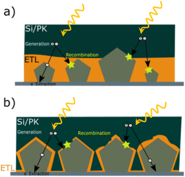 | ||
| Fig. 6 Illustration of the predicted charge separation for a metallic nanowire network used as transparent electrode in a solar cell. Schematics associated with (a) MNW diameter distribution and (b) difference of metal oxides morphology. ETL and Si/PK stand for electron transport layer and silicon/perovskites respectively. | ||
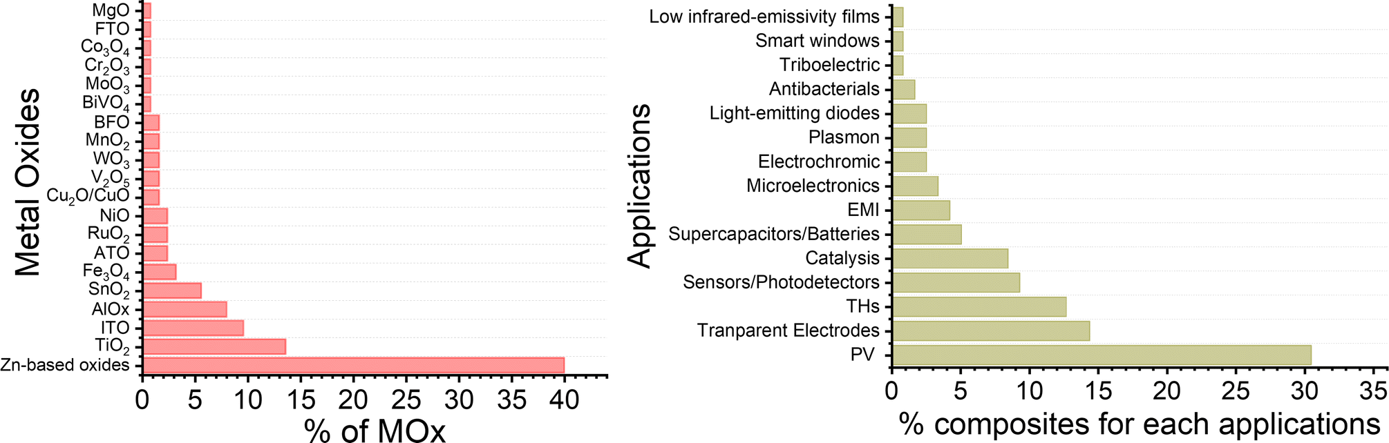 | ||
| Fig. 7 Comparison of the percentage of various MOx-coated MNNs and their different applications. The data for each graph were taken from Scopus/Web of Science July 2024. | ||
3.1 Photovoltaics (PV)
To achieve optimal performance in solar cell devices, a nanocomposite based on MOx-coated AgNW networks must meet several requirements essential for its role as transparent electrodes (TEs). The nanocomposite should possess the required electrical and optical properties, an appropriate bandgap, band alignment with the adjacent device layer, and infrared emissivity. Other important parameters include improved lateral conductivity, enhanced charge collection, and a high haze factor. These parameters will need tuning for the specific PV technology, cell architecture, and the properties of the metal oxides involved.The following section will comprehensively review reported results on various oxides to highlight their contribution in this specific application. In this context, the combination of ITO (being prepared through DC-magnetron sputtering process) and AgNW networks has been evaluated, demonstrating increased flexibility, enhanced thermal and chemical stability, and an assessment of the Schottky junction interfacial properties when combined with (p-type silicon) Si(p).51,64 Indeed, a very thin crystalline-ITO (c-ITO) layer has been combined to AgNW and CuNW networks demonstrating a power conversion efficiency of 14.15% and 12.95%, respectively, while being integrated in flexible metal halide perovskite solar cells.64
Another study has explored the electrical characteristics of AgNW networks embedded in ITO/p-Si integrated into a silicon solar cell, revealing an ideality factor of 1.58 and a quite low saturation current within the range of 5.2 × 10⁻⁵ mA cm−2.51 Further, a smooth surface with enhanced electrical and optical performance was achieved by combining c-ITO with AgNW network. The results obtained demonstrate excellent thermal and chemical stability, along with performance comparable to reference OLED and PV devices.62 ITO, a well-known material with high electrical conductivity and a bandgap and electronic affinity of approximately 3.9 eV, and an infrared emissivity coefficient of 0.2, shows promising results when combined with AgNW networks.63,94,120,121,189 Alternative metal oxides to ITO have been explored in the literature to address concerns related to material scarcity and brittleness. ZnO and AZO thin films have gained considerable interest for their versatility in a variety of solar cell structures, resulting in improvements in the optical, electrical, and mechanical properties of both electrodes and devices, as well as an extended lateral conduction range, efficient current collection, and tunable AgNW networks surface energy.61,65,93,99,100,108,111–113,119,129,130,190,191 The results obtained using AgNW networks cathodes coated with AZO and ZnO buffer layers demonstrate comparable performance to ITO, with better results observed for AZO due to its higher electrical conductivity.99 This could also be explained by the fact that AZO has a higher emissivity coefficient 0.3 at 5–20 μm compared to bare ITO.192 Another study has used a multi-stacked composite electrode configuration consisting of AZO/AgNW/AZO/ZnO for copper indium gallium selenide (CIGS) thin-film solar cells. The obtained results demonstrate superior performance compared to reference devices based on ITO/i-ZnO, attributed to enhanced lateral conductivity. This improvement can be attributed to the presence of nanowires that ensure a clear conductivity enhancement (Fig. 8a).100 Furthermore, a composite of ZnO/AgNWs has been successfully integrated into organic solar cells, resulting in a maximum power conversion efficiency (PCE) of 13.5%, surpassing that of conventional cells based on ITO. This improvement is partially attributed to enhanced conductivity and increased contact area.65 Transparent PV devices have been explored using ZnO/AgNW as top electrodes, allowing for UV-selective absorption with a PCE of 1.15% under UV and green light illumination. The combination of ZnO with the AgNW network results in improved wavelength selective absorption and photocarrier collection.66 Furthermore, ZnO nanoparticles have also been employed in perovskite solar cells, demonstrating an improvement in conductivity of the ZnO/AgNWs nanocomposites, along with an enhancement in reproducibility. This was partially attributed to the increased conductivity resulting from the full surface coverage of voids between AgNW network.193 Further, gallium-doped ZnO (GZO) combined with AgNW networks demonstrates much lower sheet resistance and a higher haze factor compared to pure GZO, with a difference of 18 Ω sq−1 and 48.2%, respectively. When this nanocomposite is integrated into a perovskite solar cell, it results in an approximately ∼21% increase in the median PCE compared to a reference device based on a pure GZO layer.172 On the other hand, fluorine-doped ZnO (FZO) presents promising electrical (20 Ω/□) and optical (90.4% at 550 nm) properties, yielding better results when coating AgNW networks compared to FTO-based perovskite solar cells.76 Ultimately, Zn2SnO4 coatings has shown an increased PCE in dye-sensitized solar cell (DSSCs) from 0.407% for reference devices to a maximum value of 1.618% when combined with the AgNW network. This was attributed in part to an improvement in the photoelectrochemical activity and charge injection.102
 | ||
| Fig. 8 Influence of the metal oxide coating MNW for photovoltaics applications and during electrical and thermal stress. (a) Schematic illustration of the electron path as a top electrode in copper indium gallium selenide (CIGS) solar cell. The left image shows the influence of the grain boundaries of AZO thin film on the transport and collection of electrons, while the right image displays the nanocomposite AZO/AgNWs,100 (b) melting of the dsDNA using AgNW/ZnO during a voltage ramp up to 4.5 V with the extrapolated temperature,3 (c) normalized resistance of bare AgNWs and NiO/AgNW on glass substrate at different annealing temperatures,106 and (d) maximum areal power density of MgO/AgNW before AgNW degradation versus MgO film thickness.81 Reproduced with permissions.3,81,100,106 | ||
Similarly, SnO2 was used to enhance the stability of AgNW networks while fine-tuning the work function. This makes SnO2 an excellent candidate for solar cells, offering higher efficiency compared to bare AgNW networks in organic PV.194 Antimony-doped tin oxide (ATO) has also been shown to enable efficiencies of around 10% in organic solar cells.136 Other MOx materials, such as TiO2 and vanadium pentoxide (V2O5) also offer great versatility and enhanced properties for solar cell devices with bandgap range of 3.0–3.2 eV and 2.04–2.44 eV respectively. They exhibit low series resistance, an enhanced built-in potential (Vbi), uniform coverage, and reduced diffuse reflection of incident light.88,89,97,114,116,117,122,186 Table 3 summarizes the optical bandgap of metal oxides coating AgNWs used for photovoltaic applications, highlighting metal oxides with wide bandgaps that minimize absorption in the visible spectrum. Key materials include indium-doped ZnO (IZO), FZO, other various Zn-based compounds, ATO, ITO, and TiO2.
| MOx/AgNW – PV application | Band gap (eV) |
|---|---|
| IZO88 | 3.2–3.45![[thin space (1/6-em)]](https://www.rsc.org/images/entities/char_2009.gif) 92,136,195,196 92,136,195,196 |
| AZO and ZnO99 | |
| AZO and ZnO multi stack100 | |
| ZnO NPs193 | |
| ZnO65 | |
| GZO172 | |
| ZnO66 | |
| Zn2SnO4 spheres102 | |
| FZO76 | |
| ITO51,62,64 | 3.5–4.3197 |
| TiO2/PEDOT:PSS89 | 3.2 (anatase) |
| TiO2 nanofibers98 | 3.0 (rutile)198,199 |
| TiO2 rutile core–shell101 | |
| Al2O380 |
6.4200–202 |
| V2O5116 |
2.04–2.44203 |
| ATO136 | 3.61–4.48204 |
Further, the nanocomposite based on PEDOT:PSS/TiO2/AgNWs achieved superior device performance compared to an ITO substrate in P3HT/PC60BM-based OPV devices. This improvement is primarily attributed to the enhanced conductivity resulting from the addition of PEDOT:PSS, while TiO2 facilitates a better connection between AgNW network.89 Furthermore, the integration of core–shell TiO2/AgNW nanocomposite into DSSCs has demonstrated enhanced light absorption and charge transport-collection efficiency while reducing recombination at the TiO2/dye/electrolyte interface. The obtained PCE is nearly 8.84%, which is 2.68% higher than reference samples based on a pure TiO2 photoanode.101 Similarly, TiO2 nanofibers (NFs)-AgNW network have shown an improved efficiency of 45.6% with respect to reference tri-layered DSSCs. The enhancement was explained through a better light absorption through scattering and local surface plasmon resonance events.98 Eventually, Al2O3 thin films have been used to coat AgNW networks by ALD and integrate them into organic solar cells, resulting in a maximum PCE of 7.03%, along with high mechanical flexibility and long-term atmospheric and thermal stability,80 thanks to its high emissivity coefficient (0.44–0.69) and high thermal expansion coefficient and elastic modulus.84,200–202
3.2 Transparent electrodes (TEs)
Other metal oxides are considered potential TEs due to their optimal optical and electrical properties, although they have not been integrated in devices. Zn-based oxides have been mostly reported with ZnO and AZO proving a great addition to the AgNW networks. ZnO-coated AgNW networks have been demonstrated to achieve a high FoM while ensuring thermal stability.115 Further, nanopyramids of ZnO are considered a great solution for coating AgNW networks, as they allow fine-tuning of the haze factor and thus the scattering properties without inducing any modification to the electrical and optical properties.205 Likewise, a sandwich structure based on AZO/AgNW/AZO demonstrates both high adhesive strength and thermal stability, showing promising potential use in PV devices.24 Indeed, AZO is shown to have high FoM with excellent long-term and mechanical stability when coated on AgNW networks.92,109 Other Zn-based doped materials have also been explored in the literature as potential candidates for PV. For instance, embedding AgNW networks in IZO results in high conductivity and transparency as well as robust mechanical properties that are well suited for flexible optoelectronics.88 In the same line, ATO-coated AgNW network offer excellent electrical and optical properties, along with mechanical flexibility with good adhesion and solvent stability.128 Moreover, ruthenium dioxide (RuO2)/AgNW TEs were fabricated through an original exfoliation approach and studied as a prospective transparent electrode. The nanocomposite demonstrates a reduction of the diffuse reflection while preventing degradation under humid air as well as a good mechanical stability.206,207 Examples of TiO2, SnO2, and Al2O3 have also been demonstrated in the literature, showing high electrical and optical properties when coating AgNW networks, along with stable features.79,95,208 Additionally, MoO3 has been shown to improve collection efficiency through better charge transport due to the enhancement of lateral conductivity.2093.3 Transparent heaters (THs)
THs based on AgNW networks are of great interest, namely for defrosting or defogging, although they exhibit some stability limitations.29 These constraints can be overcome by using MOx, which should ensure stable mechanical properties, oxidation, thermal, and chemical stability. Several materials have been explored, such as AZO, AlOx, FTO, and ITO.53,67,69,77 Combining FTO through electron cyclotron resonance MOCVD with nichrome (NiCr)/AgNW demonstrates excellent optical transmittance along with rapid thermal response, oxidation resistance, and stable mechanical properties. When integrated into THs, a decrease in surface resistance and an increase in thermal uniformity are observed.77 Similarly, the ITO/AgNW nanocomposite demonstrates highly uniform heat distribution while maintaining its functionality even at elevated applied voltages.67 THs based on AZO/AgNW nanocomposites exhibit lateral heat diffusion rather than dissipation through the air, resulting in an increased maximum temperature compared to pristine AgNW network.69 In the same way, ZnO/AgNW nanocomposite shows promising potential for in situ temperature monitoring during biological experiments, providing rapid and reproducible heating, as shown by Fig. 8b.3 In fact, ZnO enhances the current distribution by covering the voids between the AgNWs and provides excellent exothermic properties with high operating temperatures.59,78 SnO2, on the other hand, offers higher adhesion and enhanced chemical and electrical stability when coating AgNW networks.45,58,68 Similarly, a capping layer of nickel oxide (NiO) was deposited with reactive sputtering on AgNW networks for TH application, providing high passivation against atmosphere with enhanced properties (remains stable up to 185.5 °C with only a slight bias of 7 V).52 Other studies have confirmed this, as the NiO/AgNW composites fabricated by solution has shown high resistance to heating at 266 °C in the air and under harsh environment (Fig. 8c).106 The AlOx/AgNW composite has demonstrated a low sheet resistance due to an increased contact area, resulting in a rapid response and highly uniform temperature distribution.53 Similarly, AlOx/AgNW has shown highly reproducible heating performance and stability in humid environment and even for several hours under accelerated environmental stress.60,107 Further, transparent electrode based on MgO/AgNWs has demonstrated an improved thermal and electrical stability with good mechanical flexibility (Fig. 8d).81 Lastly, chromium oxide (Cr2O3) has been demonstrated to preserve the optical and electrical properties of the AgNW networks while improving the oxidative stability.2103.4 Catalysis
Several catalytic applications have been investigated in the literature. In particular, ZnO has demonstrated a slight improvement in photocatalytic activity compared to bare AgNW networks.211 Another important aspect is the morphology of MOx, as ZnO nanorods exhibit high photocatalytic properties when coating AgNW networks due to their fluffy, worm-like heteroassemblies.212 Similarly, ZnO flake-like structures show strong photoelectrochemical water splitting activity.54 TiO2 also presented some interesting features when coating AgNW networks for degrading rhodamine B solution as a photocatalyst under visible light irradiation, or for the photodegradation of phenol in water under UV light illumination.71,105 Furthermore, cuprous oxide (Cu2O) thin film has demonstrated promising catalytic performance for electrocatalytic water oxidation, while NiO with hierarchical three-dimensional morphology has shown potential as an electrocatalyst for hydrogen production in alkaline media.72,213 Other examples include non-stoichiometric WO3−x quantum dots (QDs) coating AgNW networks, which lead to improved photodegradation of methylene blue.132 Additionally, bismuth vanadate (BiVO4) has demonstrated effective charge separation and injection, while AgNW networks are employed for photoelectrochemical (PEC) water oxidation.733.5 Supercapacitors and batteries
Few studies have explored the use of MOx-coated silver nanowires in supercapacitors. Among the various MOx materials, manganese oxide (MnOx) is particularly promising. MnOx has been used as electrode in supercapacitors, significantly enhancing electrical conductivity and demonstrating excellent charge–discharge reversibility and reproducibility across a range of voltage scan rates.214 Another study by Y. Li et al. demonstrated that MnO2 with a tubular morphology contributes to enhanced electrochemical performance.215 Flexible supercapacitors have also been developed using cobalt oxide (Co3O4), which demonstrates a respectable charge storage capacity.216 In addition, bismuth ferric oxide (BFO) and RuO2 have been shown to provide excellent stability in micro-supercapacitors, offering high volumetric capacitance, energy density, and power density.75,217 Additionally, TiO2 has been used to coat AgNW networks, serving as a separator membrane in lithium-ion batteries. This coating significantly improves the discharge capacity, mechanical strength, and ionic conductivity/lithium-ion transfer number.2183.6 Sensors and photodetectors
Several studies have focused on developing sensors and photodetectors that combine AgNW networks with MOx to enhance response characteristics compared to pristine films. ZnO/AgNW nanocomposites have been introduced as efficient surface acoustic wave (SAW)-based sensor, showing enhanced responsivity and recovery characteristics compared to pristine ZnO.70 Moreover, a similar structure has proven to be efficient as an absorber layer in photodetectors with good electrical and optical properties, which can be extended to gas and/or humidity sensors.131 Other examples, such as ZnO nanoparticles combined with AgNW networks, have been tested as piezoelectric ceramics for motion detection applications,219 and quantum dot photodetectors with good response and detection features.126 Similarly, ZnO nanoflowers integrated with AgNW networks have demonstrated promising characteristics for UV photodetectors, exhibiting fast response characteristics.127 SnO2 has also been studied as a sensor when combined with AgNW networks. The whole nanocomposite was based on platinum-sensitized SnO2 nanosheets, which demonstrates a significantly high thermal stability and elevated heating capacity while sensing dimethyl sulfide (DMS) over several cycles.220 Another heterogenous structure combining SnO2/cupric oxide (CuO) offers good stability, reproducibility, accuracy, and selectivity for sulphur dioxide (SO2) gas-sensing performance.103 ITO-coated AgNW networks were also introduced as selective contact electrodes, facilitating efficient transport of photogenerated carriers due to the well-aligned energy bands in the photodetector. This resulted in an enhanced photoresponse.56 This improvement was also observed when incorporated ITO-coated AgNW networks into a Schottky photodetector, yielding a significantly increased photoresponse ratio.57 Other oxide coatings such as BFO nanoparticles and TiO2, were also used as gas sensors, allowing for enhanced sensitivity and gas surface reactions.91,2213.7 Smart windows and electrochromic applications
In other applications, such as smart windows, TiO2 displays long-time aging stability.222 The importance and intrinsic properties of the metal oxide coating towards the final functionality of the composite electrode is well illustrated in a recent study by A. Khan et al., in which SnO2/AgNW composite TE can be integrated in electrochromic devices while ZnO/AgNW ones do not result in functional devices, due to the lower chemical stability of ZnO versus SnO2.223 X. Jia et al. used ZnO-coated AgNW networks to fabricate electrochromic devices displaying quick responsiveness.134 Further, V2O5/oxide/AgNW (oxide: ZnO or SnO2) showed oxidation–reduction peaks in a Li+-based electrolyte, causing a reversible orange-to-blue colour change.223 Lastly, the introduction of WO3 to the AgNW networks improved electrical contact, demonstrating quick response and good coloration efficiency in electrochromic devices.1353.8 Electromagnetic interference shielding (EMI)
An emerging technology incorporates MOx-coated AgNW networks to prevent signal disruption by external electromagnetic interference. Iron(III) oxide (Fe3O4) is commonly used for this purpose, demonstrating promising ferromagnetic properties and enhanced EMI shielding performance, as well as improved mechanical and electrical properties.90,133,224 Zn-based oxides have also been explored for such applications. In particular, ZnO enhances sheet resistance and transmission, and significantly improves EMI. Its combination with the AgNW networks boosts electron diffusion and emission under electromagnetic waves.74 Also, zinc tin oxide (ZTO) demonstrates an improvement in the FoM and high shielding efficiency when coating AgNW networks.553.9 Microelectronics
Several MOx-coated AgNW networks have been integrated into various microelectronic devices. ITO-NP-coated AgNW networks incorporated into TFTs has demonstrated enhanced performance due to an increased charge carrier concentration.118 In metal-oxide-semiconductor devices, a sandwich structure of AZO/AgNW/AZO has been employed as an electrode, achieving excellent electrical performance and, importantly, enabling a flattening of the band voltage compared to conventional metal electrodes.85 Additionally, TiO2 combined with AgNW networks has shown excellent thermal and chemical stability, with mechanical flexibility demonstrated in TFTs.96 Another interesting application involving TiO2/AgNWs nanocomposites is the formation of transparent memristive devices with tunable switching voltage.25 In this case, the fact that the TiO2 coating is not completely efficient, results in a partial and localized spheroidization of the wires that can be used to induce memristive behaviour. Another example of resistive switching memory has been demonstrated using AZO-coated AgNW networks, which exhibit enhanced stability in flexible devices while achieving high on/off ratios.2253.10 Plasmon and light-emitting diodes (LEDs)
TiO2 has also been used for plasmonic application with a high decay time.104 Al2O3 coated AgNW networks were used to significantly tune surface plasmon resonance and reverse the polarization dependence of output intensity at the nanowire terminals.86,87 Besides, AlOx/AgNW composites have demonstrated emissivity values as low as 0.21 with a total transmittance of 78%.84 Further, UV light-emitting diodes were achieved by coating AgNW networks with AZO thin films, resulting in a significant Haacke's figure of merits.82 Ultimately, the addition of ZnO to the AgNW networks enhances the luminescence properties of flexible quantum dot LEDs.1244 Choice of metal oxide coating versus applications
As illustrated by the examples described in the previous sections, the choice of metal oxide(s) is critical for the final integration and performance of composite TEs based on AgNWs. Overall, this section thoroughly addresses various selection criteria for different applications and proposes a systematic pathway to determine the most suitable metal oxides based on specific requirements and application types. Towards this goal, Fig. 9 presents a comparison of the percentages of the various metal oxides coating AgNW networks integrated into different types of applications, with a specific focus on each application type. The figure demonstrates the predominance of Zn-based materials, followed by TiO2, ITO, AlOx, and SnO2.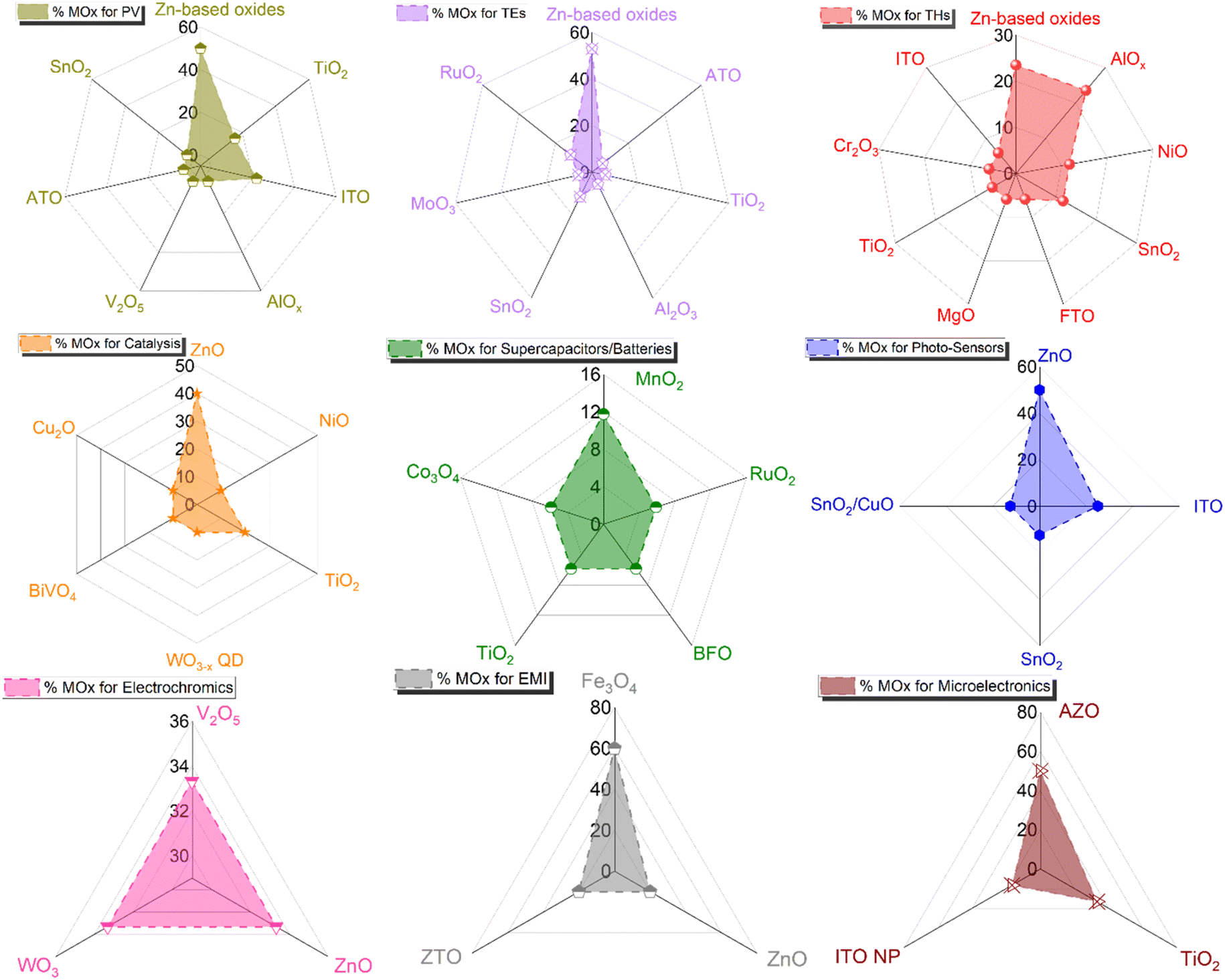 | ||
| Fig. 9 Comparison of the used metal oxides on the different applications using nanocomposites based on MOx and MNNs, along with their respective percentages. The figure illustrates general trends in various applications targeted using these nanocomposites, along with their distribution in different applications, namely, PV, TEs, THs, catalysis, supercapacitors/batteries, photodetectors/sensors, and electrochromics, among others. The marks for all criteria in each graph are data taken from Scopus/Web of Science in July 2024. | ||
4.1 Titanium oxide
In the context of PV integration, TiO2 stands out as an excellent choice due to its remarkable optical and electronic properties. Several papers have highlighted its ability in enhancing light absorption for OPV and DSSC solar cells.89,98,101 Especially, the rutile phase of TiO2 appears to be particularly advantageous due to its high absorption properties, making it particularly favourable for DSSC applications.101 Additionally, when TiO2 is combined with AgNWs, it contributes to the equilibration of the Fermi level, thereby increasing the open circuit voltage and, thus, the efficiency of the DSSC.101 This specific absorption characteristic has also proven beneficial for plasmonic applications, enabling an adjustable absorption spectrum based on the TiO2 thickness.104 Moreover, the TiO2 layer has shown to significantly improve the adhesion of the nanocomposite in smart window applications,222 the reversibility of devices in memristive technology,25 and provide good stability for AgNW during the fabrication of TFTs.96 TiO2 also stands out as an efficient separator membrane for storage applications.218 TiO2 was also demonstrated as an effective photocatalyst and gas sensor.71,105,221 To sum up, TiO2 is widely selected for a broad range of applications when combined with AgNW networks, due to its diverse and effective properties.4.2 Zn-based oxides
Other metal oxides based on Zn, namely ZnO and AZO, offer optimal electrical and optical properties demonstrating a high potential for PV applications. In fact, ZnO layers coated on AgNWs resulted in high efficiency CIGS solar cells,65 while ZnO nanoparticles showed high efficiency for PKSCs.193 Furthermore, the properties of ZnO are demonstrated to enable a reduction in dark current and hole recombination at the top surface of the cell.66 AZO, known for its higher transparency and conductivity compared to ZnO, has exhibited superior output performance in OPV devices.99 Moreover, when AZO is incorporated in a sandwich configuration with ZnO, it exhibited increased PCE in CIGS solar cells compared to ITO-based devices.100 Furthermore, the use of two AZO layers in a sandwich fashion (AZO/AgNW/AZO) enhances the mechanical flexibility of the nanocomposites designed for PV.24 Other materials based on Zn, such as IZO, FZO, and GZO, show potential for use in PV due to their low electrical resistance.76,88,172 Similarly, Zn2SnO4 spheres demonstrate high absorption characteristics for DSSC solar cells.102 ZnO has also proven effective in various photocatalytic applications due to its different structures and has shown promising features in water splitting activities.54,211,212 Further, ZnO has been employed in UV-sensor, motion detection, and photodetector applications.70,126,127,131,219 Examples were also shown for using ZnO within electrochromic device,134 and EMI application.74 Furthermore, a sandwich structure of AZO/AgNW/AZO is used as conventional metal electrodes in a metal-oxide-semiconductor device.85 AZO has proven effective in UV-LEDs due to their aforementioned favourable properties.82 Another characteristic of the AZO and ZnO layers is their stability and reproducibility, as they effectively prevent the degradation of the MNW based nanocomposites under thermal and electrical stress, particularly in TH applications.3,59,69,78 To conclude on Zn-based materials, their low electrical resistance, high optical transmittance, mechanical flexibility and ability to prevent degradation of the AgNW networks make them excellent candidates for PV, UV-LEDs/LEDs, photocatalytic, electrochromic, UV-sensors, photodetectors, motion detection, and THs.4.3 Alumina
AlOx, known for its insulating and dielectric properties, has demonstrated enhanced stability when combined with AgNW networks in organic PVSCs and polymer LEDs.80 This stability has proven beneficial in TH applications, preventing degradation under thermal and electrical stress.53,107 The AlOx layer has also been used in light-emitting diode bulbs and low infrared-emissivity films to ensure environmental stability and low-temperature coverage of the AgNW networks.83,84 In summary, the AlOx layer stands as an excellent candidate for these applications when combined to AgNW networks, providing high-stability characteristics.4.4 Indium tin oxide
Other materials such as ITO combined with AgNW and CuNW networks have demonstrated promising potential for various devices like OPV, OLEDs, PKSC, photodetectors, TFTs, and TH. This is due to their favourable electrical and optical properties compared to bare ITO and/or AgNW.51,56,57,62,64,67,1184.5 Tin oxide
SnO2 exhibited several interesting features in PV as it allows for the tunability of the work function when coated on a AgNW networks, thereby enhancing the output performance of organic solar cells.194 Additionally, it serves as an efficient and flexible TH, preventing corrosion and enabling long-term storage.68 Additionally, SnO2/AgNW was employed in sensor applications to ensure high thermal stability and heating capability.103,220 The combination of SnO2/CuO enhances sensor stability with improved selectivity and accuracy.103,2204.6 Other metal oxides
In the same line, various metal oxides have been combined with AgNW networks due to their capacity to protect against thermal and electrical stress. Examples include NiO52,106 and MgO81 for thermal and electrical stress resistance, FTO/NiCr77 for oxidation resistance. Fe3O4 is a promising candidate for coating AgNWs for EMI shielding applications due to its ferromagnetic, electrical, and mechanical properties.90,133,224 Further, RuO2 exhibits improved environmental stability and a high refractive index suitable as TEs.206 Additionally, V2O5 presents interesting multichromic features relevant to electrochromic applications.223 Cu2O, for instance, shows promising catalytic properties for OER applications.213 Overall, Table 4 summarizes the suitable metal oxides reported in the literature for various applications based on specific requirements. This table highlights the unique properties and benefits of each metal oxide, facilitating the selection process for different applications. This comparison helps guide future research based on specific application needs.| Applications | Requirements | Suitable MOx/AgNW |
|---|---|---|
| PV | Equilibration of the Fermi level | TiO2 |
| Reduction in dark current/hole recombination and good transparency/conductivity | Zn-based oxides | |
| Good electrical and optical properties | ITO and FZO | |
| Long-term atmospheric and thermal stabilities and good flexibility | AlOx | |
| Efficient current collection and tunable surface energy | ZnO | |
| Tunable work function | SnO2 | |
| TH | Ability to prevent degradation under thermal and electrical stress | Zn-based oxides and MgO |
| Enhanced thermal efficiency | ITO | |
| Protection against electrical stress, corrosion, and humidity | AlOx | |
| High thermal stability | NiO | |
| Ensure good oxidation resistance | FTO/NiCr and Cr2O3 | |
| Protection against electrical stress and corrosion | SnO2 | |
| Catalysis | High photocatalytic properties | ZnO |
| Enhances the transfer of photogenerated electron and charge separation | TiO2 | |
| Adsorption affinity and capacity | NiO and BiVO4 | |
| Fast carrier-transport | WO3−x QD | |
| OER activity | Cu2O | |
| Supercapacitors/batteries | Good conductivity and specific surface area | MnOx |
| Respectable charge storage capacity | Co3O4 | |
| Excellent stability | BFO and RuO2 | |
| Improving the discharge capacity and mechanical strength | TiO2 | |
| Sensor/photodetector | Good optical, electrical, and mechanical properties | Zn-based oxides |
| High thermal stability and heating capability | SnO2 and SnO2/CuO | |
| Efficient transport of photogenerated carriers | ITO | |
| Enhanced sensitivity and gas surface reaction | TiO2 and BFO | |
| Smart windows/electrochromic | Improved adhesion | TiO2 |
| Multichromic properties | V2O5/oxide | |
| Improved electrical contact | WO3 | |
| High chemical stability | SnO2 | |
| Low sheet resistance and high optical transmittance | ZnO | |
| Electromagnetic interference shielding | Ferromagnetic properties and good mechanical/electrical properties | Fe3O4 |
| High FoM | ZTO and ZnO | |
| Plasmon/LEDs | Tuning the plasmon resonance and low emissivity | AlOx |
| Improved luminescence properties | ZnO | |
| Adjustable absorption spectra | TiO2 | |
| Microelectronics | Thermal and chemical stability | TiO2 |
| Switching voltages | TiO2 | |
| Enhanced charge carrier concentration | ITO | |
| Good electrical properties and stability | ZnO and AZO |
5 Conclusive remarks and prospects
The potential of AgNW networks is widely demonstrated within the literature (low operating and fabrication cost, flexibility, and transparency), as it paves the way for the next generation of transparent conductive materials that can be easily implemented in various application fields such as photovoltaics, touch screens, transparent heaters, low-emissivity coatings, among others. Despite these numerous advantages, metallic nanowire networks face stability issues that can impede device efficiency and operational stability, hindering their widespread adoption in the industry. To overcome these issues, several studies have focused on investigating coatings based on thin film metal oxides, aiming to enhance the lifetime stability of metallic nanowires-based devices. Moreover, these coatings offer the flexibility to finely tune the optical and electrical properties of the nanocomposites, thereby providing adjustable functionalities. Towards this purpose, it is necessary to adjust regarding metal oxide characteristics and conformality, based on the specific requirements. By combining the optical properties of both materials, light absorption can be shifted to meet specific constraint in various optoelectronic applications. This is the case of intrinsic ZnO and ZnO:Al that has been integrated in photovoltaic application to enhance the electrical conductivity and optical transmittance.65,99,100,193 Furthermore, metal oxides such as TiO2 or IZO have also shown enhanced adhesion and electrical conductivity, resulting in a significant improvement in surface roughness and thermal stability.88,89In fact, there are several remaining challenges that need to be addressed, and it is crucial to make an appropriate selection of the coating for the targeted application. The goal is to prioritize various parameters associated with the coating, such as conformality, coating nature, thickness, properties, as well as the desired functionalities. Therefore, choosing the right coating for the intended application becomes essential. This selection process should also consider factors like coating efficiency, cost, and environmental impact based on the coating process employed. In this sense, a recent study by M. Weber et al. evaluated the environmental impact of ALD and proposes different strategies to minimizing it.226 One of them is precisely moving to SALD, since the faster deposition is also beneficial in terms of environmental impact.223 Another effective strategy would involve implementing a combinatorial approach to select the optimal coating metal oxides based on various parameters such as film thickness, surface roughness, and adhesion, as well as properties like electrical, optical, and thermal characteristics.223,227,228 This approach holds significant promise, particularly with the advancements in artificial intelligence and machine learning within the fields of material engineering and science.229,230 Moreover, it can serve as a valuable asset for investigating the influence of integrating new metal oxide coatings onto metallic nanowires. This combination has the potential to expand the range of applications, allowing for fine-tuning of the work function and band alignment in optoelectronic devices and enhancing the stability of all applications. The information obtained from these investigations will be valuable for future technologies. To that end, several perspectives are proposed:
• As shown in this review, the most studied MNN so far are based on AgNW networks, while other metallic nanowire could be of interest, such as CuNW or core shell structure such as, Cu@NiNW. However, the latter exhibits much less stability (thermal or chemical). Further developments are of crucial significance, as the use of CuNW networks, for instance (instead of AgNW networks), could be highly advantageous. Cu is not only more cost-effective but also much more abundant than Ag. MOx coating should help in this regard thanks to the stability enhancement.
• Process optimization is necessary to incorporate plasma and UV assistance during metal oxide growth, aiming to reduce the metal oxide deposition temperature. This would facilitate the integration and testing of new metal oxide coatings, and the possibility to efficiently coat MNN on temperature sensitive substrates (such as polymers) or devices (such as perovskite-based solar cells).
• Careful consideration should be given to the economic cost at the process level and chemical efficiency. The cost and quality of the coatings will vary depending on the chosen process. The microstructure of the coating (thus the choice of the process) should also be tailored according to the intended application.
• Environmental impact is a crucial factor. Additional efforts should be made in precursor synthesis and reducing energy waste associated with the chosen process. As stated above, a recent pertinent example of such approach concerns the assessment of the environmental impact of ALD, considering the green chemistry and the specificities of the ALD process, and suggesting future pathways to reduce the ALD environmental impact.226 Such works can help in designing metal oxide coating methods compatible with greener chemistry and considering the coating method sustainability.
• Further developments should also focus on precise control and optimization of all parameters, enabling large-scale scalability for industrial applications. This would create opportunities for the fabrication of various devices on a large scale.
Taking all of the above into account, there are several aspects that need to be explored in the coming years. Numerous research groups are already working towards enhancing these key points, and clear strategies have been identified. The field is progressing rapidly, and the development of these nanocomposites for real industrial applications is expected to advance. Such research is associated to significant efforts that are still required to overcome challenges related to device integration and operational stability.
Data availability
No primary research results, software or code have been included and no new data were generated or analysed as part of this review.Conflicts of interest
There are no conflicts to declare.Acknowledgements
The authors acknowledge the Agence Nationale de la Recherche (ANR, France) via the project ANR-23-CE051-0038 LESMENINES, ANR-21-MERA-0001-01 INSTEAD, ANR-21-CE08-0047 REACTIVE, and ANR-22-PETA-0011 SOLSTICE. We thank the PhosAgro/UNESCO/IUPAC research grant in green chemistry for funding through project 096 (No. 4500461756).Notes and references
- H. Kang, S. Jung, S. Jeong, G. Kim and K. Lee, Nat. Commun., 2015, 6, 1–7 Search PubMed.
- A. Anand, M. M. Islam, R. Meitzner, U. S. Schubert and H. Hoppe, Adv. Energy Mater., 2021, 11, 2100875 CrossRef CAS.
- D. T. Papanastasiou, A. Sekkat, V. H. Nguyen, C. Jiménez, D. Muñoz-rojas, F. Bruckert and D. Bellet, Adv. Mater. Technol., 2022, 8, 2200563 CrossRef.
- T. Sannicolo, M. Lagrange, A. Cabos, C. Celle, J. Simonato and D. Bellet, Small, 2016, 12, 6052–6075 CrossRef CAS.
- A. Cruz, E. C. Wang, A. B. Morales-Vilches, D. Meza, S. Neubert, B. Szyszka, R. Schlatmann and B. Stannowski, Sol. Energy Mater. Sol. Cells, 2019, 195, 339–345 CrossRef.
- H. Jin, C. Tao, M. Velusamy, M. Aljada, Y. Zhang, M. Hambsch, P. L. Burn and P. Meredith, Adv. Mater., 2012, 24, 2572–2577 CrossRef CAS.
- K. Ellmer, Nat. Photonics, 2012, 6, 809–817 CrossRef CAS.
- P. Doggart, N. Bristow and J. Kettle, J. Appl. Phys., 2014, 116, 103103 CrossRef.
- G. Rey, C. Ternon, M. Modreanu, X. Mescot, V. Consonni and D. Bellet, J. Appl. Phys., 2013, 114, 183713 CrossRef.
- M. N. Gueye, A. Carella, J. Faure-Vincent, R. Demadrille and J. P. Simonato, Prog. Mater. Sci., 2020, 108, 100616 CrossRef CAS.
- M. Mirabedin, H. Vergnes, N. Caussé, C. Vahlas and B. Caussat, Appl. Surf. Sci., 2021, 554, 149501 CrossRef CAS.
- A. Sekkat, H. El Housseiny, E. Poupaki, B. Breig, D. Sam, O. Marsan, C. Charvillat, A. Pugliara, N. Causs, H. Vergnes, M. Ternisien, C. Renaud, G. Zissis and B. Caussat, ACS Appl. Polym. Mater., 2023, 5, 10205–10216 CrossRef CAS.
- J. Cameron and P. J. Skabara, Mater. Horiz., 2020, 7, 1759–1772 RSC.
- Y. Chen, H. Yang, Z. Han, Z. Bo, J. Yan, K. Cen and K. K. Ostrikov, Energy Fuels, 2022, 36, 2390–2406 CrossRef CAS.
- M. M. Hossain, B. M. Li, B. Sennik, J. S. Jur and P. D. Bradford, npj Flexible Electron., 2022, 6, 97 CrossRef CAS.
- V. H. Nguyen, D. T. Papanastasiou, J. Resende, L. Bardet, T. Sannicolo, C. Jiménez, D. Muñoz-Rojas, N. D. Nguyen and D. Bellet, Small, 2022, 18, 2106006 CrossRef CAS.
- D. P. Langley, M. Lagrange, G. Giusti, C. Jiménez, Y. Bréchet, N. D. Nguyen and D. Bellet, Nanoscale, 2014, 6, 13535–13543 RSC.
- J. J. Patil, W. H. Chae, A. Trebach, K. J. Carter, E. Lee, T. Sannicolo and J. C. Grossman, Adv. Mater., 2021, 33, 1–29 CrossRef.
- M. Rothe, Y. Zhao, G. Kewes, Z. Kochovski, W. Sigle, P. A. van Aken, C. Koch, M. Ballauff, Y. Lu and O. Benson, Sci. Rep., 2019, 9, 1–12 CrossRef CAS.
- Y. Zhang, Z. Lu, X. Zhou and J. Xiong, Mater. Today, 2024, 73, 179–207 CrossRef CAS.
- J. Yang, F. Yu, A. Chen, S. Zhao, Y. Zhou, S. Zhang, T. Sun and G. Hu, Adv. Powder Mater., 2022, 1, 100045 CrossRef.
- T. Zhang, M. Zhao, F. Daneshvar, F. Xia and H. J. Sue, ACS Appl. Nano Mater., 2019, 2, 7775–7784 CrossRef CAS.
- H. Ha, C. Amicucci, P. Matteini and B. Hwang, Colloid Interface Sci. Commun., 2022, 50, 100663 CrossRef.
- Q. Xu, W. Shen, Q. Huang, Y. Yang, R. Tan, K. Zhu, N. Dai and W. Song, J. Mater. Chem. C, 2014, 2, 3750–3755 RSC.
- J. A. Resende, A. Sekkat, V. H. Nguyen, T. Chatin, C. Jiménez, M. Burriel, D. Bellet and D. Muñoz-Rojas, Small, 2021, 2007344, 1–8 Search PubMed.
- P. Maisch, K. C. Tam, L. Lucera, H. J. Egelhaaf, H. Scheiber, E. Maier and C. J. Brabec, Org. Electron., 2016, 38, 139–143 CrossRef CAS.
- S. Zhang, X. Liu, T. Lin and P. He, J. Mater. Sci.: Mater. Electron., 2019, 30, 18702–18709 CrossRef CAS.
- D. Langley, G. Giusti, C. Mayousse, C. Celle, D. Bellet and J. P. Simonato, Nanotechnology, 2013, 24, 452001 CrossRef.
- D. T. Papanastasiou, A. Schultheiss, D. Muñoz-Rojas, C. Celle, A. Carella, J. P. Simonato and D. Bellet, Adv. Funct. Mater., 2020, 30, 1–33 CrossRef.
- J. Yun, Adv. Funct. Mater., 2017, 27, 1606641 CrossRef.
- L. Bardet, D. T. Papanastasiou, C. Crivello, M. Akbari, J. Resende, A. Sekkat, C. Sanchez-Velasquez, L. Rapenne, C. Jiménez, D. Muñoz-Rojas, A. Denneulin and D. Bellet, Nanomaterials, 2021, 11, 2785 CrossRef CAS PubMed.
- T. Sannicolo, N. Charvin, L. Flandin, S. Kraus, D. T. Papanastasiou, C. Celle, J. P. Simonato, D. Muñoz-Rojas, C. Jiménez and D. Bellet, ACS Nano, 2018, 12, 4648–4659 CrossRef CAS PubMed.
- B. Deng, P. C. Hsu, G. Chen, B. N. Chandrashekar, L. Liao, Z. Ayitimuda, J. Wu, Y. Guo, L. Lin, Y. Zhou, M. Aisijiang, Q. Xie, Y. Cui, Z. Liu and H. Peng, Nano Lett., 2015, 15, 4206–4213 CrossRef CAS PubMed.
- V. H. Nguyen, Development of transparent electrodes by vacuum-free and low cost deposition methods for photovoltaic applications, UGA, 2019 Search PubMed.
- H. J. Yun, S. J. Kim, J. H. Hwang, Y. S. Shim, S. G. Jung, Y. W. Park and B. K. Ju, Sci. Rep., 2016, 6, 1–12 CrossRef CAS PubMed.
- S. Aghazadehchors, Metallic nanowire networks : silver nanowire network stability enhancement using metal oxide coatings, Percolation onset of nano-object network, UGA, 2022 Search PubMed.
- S. Patil, P. R. Kate, J. B. Deshpande and A. A. Kulkarni, Chem. Eng. J., 2021, 414, 128711 CrossRef CAS.
- T. Cheng, Y. Zhang, W. Lai, Y. Chen and W. Huang, Chin. J. Chem., 2015, 33, 147–151 CrossRef CAS.
- C. Mayousse, C. Celle, E. Moreau, J. F. Mainguet, A. Carella and J. P. Simonato, Nanotechnology, 2013, 24, 215501 CrossRef.
- A. Kumar, M. Kumar, M. S. Goyat and D. K. Avasthi, Mater. Today Commun., 2022, 33, 104433 CrossRef CAS.
- E. Carlos, R. Branquinho, R. Martins, A. Kiazadeh and E. Fortunato, Adv. Mater., 2021, 33, 1–37 Search PubMed.
- S. J. Zou, Y. Shen, F. M. Xie, J. De Chen, Y. Q. Li and J. X. Tang, Mater. Chem. Front., 2020, 4, 788–820 RSC.
- L. Bardet, H. Roussel, S. Saroglia, M. Akbari, D. Muñoz-Rojas, C. Jiménez, A. Denneulin and D. Bellet, Nanoscale, 2023, 16, 564–579 RSC.
- T. Sannicolo, D. Muñoz-Rojas, N. D. Nguyen, S. Moreau, C. Celle, J. P. Simonato, Y. Bréchet and D. Bellet, Nano Lett., 2016, 16, 7046–7053 CrossRef CAS PubMed.
- L. Bardet, M. Akbari, C. Crivello, L. Rapenne, M. Weber, V. H. Nguyen, C. Jiménez, D. Muñoz-Rojas, A. Denneulin and D. Bellet, ACS Appl. Nano Mater., 2023, 6, 15234–15246 CrossRef CAS.
- Y. Won, A. Kim, W. Yang, S. Jeong and J. Moon, NPG Asia Mater., 2014, 6, e132 CrossRef CAS.
- J. Bang, S. Coskun, K. R. Pyun, D. Doganay, S. Tunca, S. Koylan, D. Kim, H. E. Unalan and S. H. Ko, Appl. Mater. Today, 2021, 22, 100909 CrossRef.
- N. Kaur, M. Singh and E. Comini, Adv. Mater. Interfaces, 2022, 9, 2101629 CrossRef CAS.
- J. Liu, D. Jia, J. M. Gardner, E. M. J. Johansson and X. Zhang, Mater. Today Energy, 2019, 13, 152–185 CrossRef.
- Q. Zhao, Y. Fang, K. Qiao, W. Wei, Y. Yao and Y. Gao, Sol. Energy Mater. Sol. Cells, 2019, 194, 95–102 CrossRef CAS.
- P. Mahala, M. Patel, N. Gupta, J. Kim and B. H. Lee, Phys. B, 2018, 537, 228–235 CrossRef CAS.
- M. Patel, K. R. Chauhan, J. Kim, J. W. Kim and D. Lim, Sens. Actuators, A, 2017, 267, 8–13 CrossRef CAS.
- J. M. Lee, Y. H. Kim, H. K. Kim, H. J. Kim and C. H. Hong, Sci. Rep., 2020, 10, 1–8 CrossRef CAS.
- A. Sreedhar, I. N. Reddy, Q. T. Hoai Ta, G. Namgung, E. Cho and J. S. Noh, Ceram. Int., 2019, 45, 6985–6993 CrossRef CAS.
- K. Jenifer and S. Parthiban, Nanotechnology, 2024, 35, 305205 Search PubMed.
- S. Abbas, M. Kumar, D. W. Kim and J. Kim, Small, 2019, 15, 1–9 CrossRef PubMed.
- H. S. Kim, M. Patel, H. H. Park and J. Kim, Sens. Actuators, A, 2016, 247, 215–220 CrossRef CAS.
- K. Zhou, Y. Hu, Y. Chen, Z. Hu, Y. Hu, W. Liu and Z. Min, Ceram. Int., 2023, 49, 14530–14537 CrossRef CAS.
- M. Patel, J. H. Seo, S. Kim, T. T. Nguyen, M. Kumar, J. Yun and J. Kim, J. Power Sources, 2021, 491, 1–10 CrossRef.
- M. Hu, Z. Sun, Z. Qiu, L. Zhao, L. Song, Q. Dong and S. Yu, Curr. Appl. Phys., 2024, 66, 115–121 CrossRef.
- M. Patel, J. H. Seo, T. T. Nguyen and J. Kim, Cell Rep. Phys. Sci., 2021, 2, 100591 CrossRef CAS.
- H. G. Im, J. Jang, Y. Jeon, J. Noh, J. Jin, J. Y. Lee and B. S. Bae, ACS Appl. Mater. Interfaces, 2020, 12, 56462–56469 CrossRef CAS.
- H. S. Kim, M. Patel, H. H. Park, A. Ray, C. Jeong and J. Kim, ACS Appl. Mater. Interfaces, 2016, 8, 8662–8669 CrossRef CAS PubMed.
- H. G. Im, S. Jeong, J. Jin, J. Lee, D. Y. Youn, W. T. Koo, S. B. Kang, H. J. Kim, J. Jang, D. Lee, H. K. Kim, I. D. Kim, J. Y. Lee and B. S. Bae, NPG Asia Mater., 2016, 8, e282 CrossRef CAS.
- M. Singh, T. R. Rana, S. Kim, K. Kim, J. H. Yun and J. Kim, ACS Appl. Mater. Interfaces, 2016, 8, 12764–12771 CrossRef CAS.
- J. Song, M. Patel, S. E. Johannesson, K. Cho, J. Park, J. Kim and D. W. Kim, Adv. Electron. Mater., 2023, 9, 2300326 CrossRef CAS.
- H. G. Cheong, D. W. Song and J. W. Park, Microelectron. Eng., 2015, 146, 11–18 CrossRef CAS.
- S. Yu, X. Liu, H. Dong, X. Wang and L. Li, Ceram. Int., 2021, 47, 20379–20386 CrossRef CAS.
- H. G. Cheong, J. H. Kim, J. H. Song, U. Jeong and J. W. Park, Thin Solid Films, 2015, 589, 633–641 CrossRef CAS.
- M. B. Jeon, Y. H. Kwak, B. K. Ju and K. Kim, Sens. Actuators, A, 2020, 311, 112044 CrossRef CAS.
- T. Tang, T. Wang, Y. Gao, H. Xiao and J. Xu, J. Mater. Sci.: Mater. Electron., 2019, 30, 8471–8478 CrossRef CAS.
- K. L. Zhou, Z. Wang, C. B. Han, X. Ke, C. Wang, Y. Jin, Q. Zhang, J. Liu, H. Wang and H. Yan, Nat. Commun., 2021, 12, 1–10 CrossRef PubMed.
- S. Zhang, H. Zhang, Y. Gu, X. Mao, X. Gao and D. Xu, Fuel, 2024, 370, 131847 CrossRef CAS.
- S. Yan, H. Wang and P. Li, CrystEngComm, 2022, 24, 6622–6627 RSC.
- D. Choi, B. H. An, M. Mansouri, D. Ali, M. Khalil, K. Xu, D. Nwoke, J. R. Park, A. Shankar and J. E. Ryu, J. Compos. Mater., 2017, 51, 965–969 CrossRef CAS.
- J. Han, S. Yuan, L. Liu, X. Qiu, H. Gong, X. Yang, C. Li, Y. Hao and B. Cao, J. Mater. Chem. A, 2015, 3, 5375–5384 RSC.
- A. Y. Kim, M. K. Kim, C. Hudaya, J. H. Park, D. Byun, J. C. Lim and J. K. Lee, Nanoscale, 2016, 8, 3307–3313 RSC.
- K. W. Seo, M. Y. Kim, H. S. Chang and H. K. Kim, AIP Adv., 2015, 5, 127132 Search PubMed.
- C. Lee, H. Kim and B. Hwang, J. Alloys Compd., 2019, 773, 361–366 CrossRef CAS.
- S. Wang, S. Wu, Z. Ling, H. Chen, H. Lian, X. Portier, F. Gourbilleau, T. Marszalek, F. Zhu, B. Wei and T. Xu, Org. Electron., 2020, 78, 105593 CrossRef CAS.
- A. Sekkat, D. T. Papanastasiou, M. A. Ghani, H. Roussel, M. Weber, L. Rapenne, C. Jiménez, D. Muñoz-Rojas and D. Bellet, Adv. Mater. Technol., 2023, 2301143, 1–8 Search PubMed.
- X. Yan, J. Ma, H. Xu, C. Wang and Y. Liu, J. Phys. D Appl. Phys., 2016, 49, 325103 CrossRef.
- B. Hwang, Y. An, H. Lee, E. Lee, S. Becker, Y. H. Kim and H. Kim, Sci. Rep., 2017, 7, 1–7 CrossRef CAS.
- S. Hanauer, C. Celle, C. Crivello, H. Szambolics, D. Muñoz-Rojas, D. Bellet and J. P. Simonato, ACS Appl. Mater. Interfaces, 2021, 13, 21971–21978 CrossRef CAS PubMed.
- G. Zhang, M. Zheng, J. Wan, H. Wu and C. Liu, Appl. Surf. Sci., 2019, 469, 98–102 CrossRef CAS.
- H. Wei, D. Pan and H. Xu, Nanoscale, 2015, 7, 19053–19059 RSC.
- H. Wei, S. Zhang, X. Tian and H. Xu, Appl. Phys. Sci., 2013, 12, 4494–4499 Search PubMed.
- W. J. Scheideler, J. Smith, I. Deckman, S. Chung, A. C. Arias and V. Subramanian, J. Mater. Chem. C, 2016, 4, 3248–3255 RSC.
- R. Zhu, C. H. Chung, K. C. Cha, W. Yang, Y. B. Zheng, H. Zhou, T. B. Song, C. C. Chen, P. S. Weiss, G. Li and Y. Yang, ACS Nano, 2011, 5, 9877–9882 CrossRef CAS.
- Y. Tan, Y. Xue, K. Li, S. Liu, F. Tan, X. Wu, Q. Qin, T. Lei, Y. Yang, S. Qin and D. Zhang, Polym. Compos., 2023, 1–16 Search PubMed.
- S. Patil, S. Arumugam and P. Swaminathan, ACS Omega, 2024, 9, 28978–28988 CrossRef CAS.
- K. Lin, C. Wu, H. Zhang, X. Yu, M. Li, Z. Li, X. Yu, Y. Cao, Q. Qiao and Y. Zhou, Mater. Lett., 2023, 337, 133951 CrossRef CAS.
- W. Pan, Y. Han, Z. Wang, C. Gong, J. Guo, J. Lin, Q. Luo, S. Yang and C. Q. Ma, J. Mater. Chem. A, 2021, 9, 16889–16897 RSC.
- A. Kim, H. Lee, H. C. Kwon, H. S. Jung, N. G. Park, S. Jeong and J. Moon, Nanoscale, 2016, 8, 6308–6316 CAS.
- B. Bob, A. Machness, T. B. Song, H. Zhou, C. H. Chung and Y. Yang, Nano Res., 2016, 9, 392–400 CrossRef CAS.
- T. B. Song, Y. S. Rim, F. Liu, B. Bob, S. Ye, Y. T. Hsieh and Y. Yang, ACS Appl. Mater. Interfaces, 2015, 7, 24601–24607 CrossRef CAS PubMed.
- H. K. H. D. Kankanamge, J. M. K. W. Kumari, M. A. K. L. Dissanayake, G. K. R. Senadeera, B. S. Dassanayake and H. C. S. Perera, Bull. Mater. Sci., 2023, 46, 5–8 Search PubMed.
- M. G. C. M. Kumari, C. S. Perera, B. S. Dassanayake, M. A. K. L. Dissanayake and G. K. R. Senadeera, Electrochim. Acta, 2019, 298, 330–338 CrossRef CAS.
- T. Stubhan, J. Krantz, N. Li, F. Guo, I. Litzov, M. Steidl, M. Richter, G. J. Matt and C. J. Brabec, Sol. Energy Mater. Sol. Cells, 2012, 107, 248–251 CrossRef CAS.
- A. Kim, Y. Won, K. Woo, S. Jeong and J. Moon, Adv. Funct. Mater., 2014, 24, 2462–2471 CrossRef CAS.
- H. Dong, Z. Wu, F. Lu, Y. Gao, A. El-shafei, B. Jiao, S. Ning and X. Hou, Nano Energy, 2014, 10, 181–191 CAS.
- D. Ursu, R. Banică, M. Vajda, C. B. Baneasa and M. Miclau, J. Alloys Compd., 2022, 902, 163890 CrossRef CAS.
- J. Yang, T. Wang, C. Zhu, X. Yin, P. Dong and X. Wu, Sens. Actuators, B, 2023, 375, 132966 CrossRef CAS.
- J. Cheng, Y. Li, M. Plissonneau, J. Li, J. Li, R. Chen, Z. Tang, L. Pautrot-d'Alençon, T. He, M. Tréguer-Delapierre and M. H. Delville, Sci. Rep., 2018, 8, 1–11 Search PubMed.
- X. B. Xiang, Y. Yu, W. Wen and J. M. Wu, New J. Chem., 2018, 42, 265–271 RSC.
- L. Song, S. Qu and S. Yu, ACS Appl. Nano Mater., 2023, 6, 12413–12424 CrossRef CAS.
- D. T. Papanastasiou, E. Carlos, D. Muñoz-Rojas, C. Jiménez, A. Pimentel, E. Fortunato, R. Martins and D. Bellet, ACS Appl. Electron. Mater., 2022, 4, 5816–5824 CrossRef CAS.
- X. Chen, G. Xu, G. Zeng, H. Gu, H. Chen, H. Xu, H. Yao, Y. Li, J. Hou and Y. Li, Adv. Mater., 2020, 32, 1–10 Search PubMed.
- J. Liu, M. Xu, J. Li, T. Zhang, X. Chu, F. Jin, Y. Zhai, K. Shi and D. Lu, J. Mater. Sci.: Mater. Electron., 2020, 31, 4178–4183 CrossRef CAS.
- S. Bai, X. Guo, T. Chen, Y. Zhang and H. Yang, Thin Solid Films, 2020, 709, 138096 CrossRef CAS.
- H. Liu, J. Wu, Y. Fu, B. Wang, Q. Yang, G. D. Sharma, M. L. Keshtov and Z. Xie, Thin Solid Films, 2021, 718, 138486 CrossRef CAS.
- M. Singh, P. Prasher and J. Kim, Nano-Struct. Nano-Objects, 2018, 16, 151–155 CrossRef CAS.
- E. Lee, J. Ahn, H. C. Kwon, S. Ma, K. Kim, S. Yun and J. Moon, Adv. Energy Mater., 2018, 8, 1702182 CrossRef.
- J. H. Yim, S. Y. Joe, C. Pang, K. M. Lee, H. Jeong, J. Y. Park, Y. H. Ahn, J. C. de Mello and S. Lee, ACS Nano, 2014, 8, 2857–2863 CrossRef CAS PubMed.
- Y. J. Shiau, K. M. Chiang and H. W. Lin, Nanoscale, 2015, 7, 12698–12705 RSC.
- E. Ngo, S. Venkatesan and Q. Qiao, IEEE Trans. Electron Devices, 2014, 61, 2957–2962 CAS.
- C. C. Chen, L. Dou, R. Zhu, C. H. Chung, T. B. Song, Y. B. Zheng, S. Hawks, G. Li, P. S. Weiss and Y. Yang, ACS Nano, 2012, 6, 7185–7190 CrossRef CAS PubMed.
- C. Kim, Y. H. Kim, Y. Y. Noh, S. J. Hong and M. J. Lee, Adv. Electron. Mater., 2018, 4, 1700440 CrossRef.
- Z. M. Beiley, M. G. Christoforo, P. Gratia, A. R. Bowring, P. Eberspacher, G. Y. Margulis, C. Cabanetos, P. M. Beaujuge, A. Salleo and M. D. McGehee, Adv. Mater., 2013, 25, 7020–7026 CrossRef CAS PubMed.
- C. H. Chung, B. Bob, T. B. Song and Y. Yang, Sol. Energy Mater. Sol. Cells, 2014, 120, 642–646 CrossRef CAS.
- C. H. Chung, T. B. Song, B. Bob, R. Zhu, H. S. Duan and Y. Yang, Adv. Mater., 2012, 24, 5499–5504 CrossRef CAS PubMed.
- T. Y. Chen, C. M. Fan, J. Y. Wu and T. L. Lin, J. Chin. Chem. Soc., 2009, 56, 1244–1249 CrossRef CAS.
- Z. Xia, X. Lei, Y. Hu, X. Liu, Y. Ji, D. Zhang, Y. Cheng, X. Liu, Z. Xu, X. Yang, J. Zhong and W. Huang, Sol. RRL, 2024, 8, 2400230 CrossRef CAS.
- Y. Fang, K. Ding, Z. Wu, H. Chen, W. Li, S. Zhao, Y. Zhang, L. Wang, J. Zhou and B. Hu, ACS Nano, 2016, 10, 10023–10030 CrossRef CAS PubMed.
- K. Y. Shin, S. Kim, M. J. Keum and K. H. Kim, J. Nanosci. Nanotechnol., 2017, 17, 7449–7453 CrossRef CAS.
- M. Savas, A. F. Yazici, A. Arslan, E. Mutlugün and T. Erdem, Opt. Eng., 2023, 62, 1–14 Search PubMed.
- M. Kumar, H. Jeong and D. Lee, Superlattices Microstruct., 2019, 126, 132–138 CrossRef CAS.
- G. Sin, K. Ri, S. Jon and G. Kim, Eng. Res. Express, 2024, 6, 025006 CrossRef.
- J. J. Kim, K. Shuji, J. Zheng, X. He, A. Sajjad, H. Zhang, H. Su and W. C. H. Choy, Nat. Commun., 2024, 15, 1–10 Search PubMed.
- L. Zheng, M. Li, S. Dai, Y. Wu, Y. Cai, X. Zhu, S. Ma, D. Yun and J. F. Li, J. Phys. Chem. C, 2021, 125, 18623–18629 CrossRef CAS.
- N. M. Nair, M. M. Jahanara, D. Ray and P. Swaminathan, Flexible Printed Electron., 2021, 6, 045004 CrossRef CAS.
- W. Wei, Y. Yao, Q. Zhao, Z. Xu, Q. Wang, Z. Zhang and Y. Gao, Nanoscale, 2019, 11, 5535–5547 RSC.
- X. Chen, C. Wu, W. Luo, L. Li, L. Xie and B. Xue, Surf. Interfaces, 2024, 49, 104439 CrossRef CAS.
- X. Jia, P. Yang, L. Zhao, D. Du, Z. Wang, W. An and S. Yu, ACS Appl. Electron. Mater., 2023, 5, 4198–4208 CrossRef CAS.
- D. K. An and S. J. Jeon, Korean J. Chem. Eng., 2024, 41, 2173–2181 CrossRef CAS.
- E. Georgiou, A. Ioakeimidis, I. Antoniou, I. T. Papadas, A. Hauser, M. Rossier, F. Linardi and S. A. Choulis, ACS Appl. Electron. Mater., 2022, 5, 181–188 CrossRef PubMed.
- A. Baptista, F. Silva, J. Porteiro, J. Míguez and G. Pinto, Coatings, 2018, 8, 402 CrossRef.
- P. J. Kelly and R. D. Arnell, Vacuum, 2000, 56, 159–172 CrossRef CAS.
- S. M. Rossnagel, IBM J. Res. Dev., 1999, 43, 163–179 CAS.
- T. Fix, Dépôt par ablation laser pulsé, Tech. l’ingénieur, 2021, p. E4216 Search PubMed.
- A. J. Haider, T. Alawsi, M. J. Haider, B. A. Taha and H. A. Marhoon, Opt. Quantum Electron., 2022, 54, 1–25 CrossRef.
- A. Jaud, S. Ponton, A. Sekkat, A. A. Aal, T. Sauvage, D. Samelor, H. Vergnes, B. Diallo, J. Etzkorn, B. Caussat and C. Vahlas, Surf. Coat. Technol., 2023, 462, 129476 CrossRef CAS.
- F. Weiss, M. Audier, A. Bartasyte, D. Bellet, C. Girardot, C. Jimenez, J. Kreisel, S. Pignard, M. Salaun and C. Ternon, Pure Appl. Chem., 2009, 81, 1523–1534 CAS.
- H. Frey, Handbook of Thin Film Technology, 2015, pp. 225–252 Search PubMed.
- S. M. George, Chem. Rev., 2010, 110, 111–131 CrossRef CAS PubMed.
- E. des Ligneris, D. Samélor, A. Sekkat, C. Josse, T. Hungria, A. Pugliara, C. Vahlas and B. Caussat, J. Vac. Sci. Technol., A, 2024, 42, 032408 CrossRef CAS.
- G. N. Parsons, S. M. George and M. Knez, MRS Bull., 2011, 36, 865–871 CrossRef CAS.
- M. J. Weber, M. A. Verheijen, A. A. Bol and W. M. M. Kessels, Nanotechnology, 2015, 26, 094002 CrossRef CAS PubMed.
- A. Frechilla, A. Sekkat, M. Dibenedetto, F. lo Presti, L. Porta-Velilla, E. Martínez, G. F. de La Fuente, L. A. Angurel and D. Muñoz-Rojas, Mater. Today Adv., 2023, 19, 10041 Search PubMed.
- J. P. Vale, A. Sekkat, T. Gheorghin, S. Sevim, E. Mavromanolaki, A. D. Flouris, S. Pané, D. Muñoz-Rojas, J. Puigmartí-Luis and T. Sotto Mayor, J. Phys. Chem. C, 2023, 127, 9425–9436 CrossRef CAS PubMed.
- D. Muñoz-Rojas, T. Maindron, A. Esteve, F. Piallat, J. C. S. S. Kools and J. M. Decams, Mater. Today Chem., 2019, 12, 96–120 CrossRef.
- D. Muñoz-Rojas and J. Macmanus-Driscoll, Mater. Horiz., 2014, 1, 314–320 RSC.
- P. Poodt, D. C. Cameron, E. Dickey, S. M. George, V. Kuznetsov, G. N. Parsons, F. Roozeboom, G. Sundaram and A. Vermeer, J. Vac. Sci. Technol., A, 2012, 30, 010802 CrossRef.
- V. S. Nguyen, A. Sekkat, D. Bellet, G. Chichignoud, A. Kaminski-cachopo, D. Muñoz-Rojas, W. Favre, D. Muñoz-Rojas and W. Favre, J. Mater. Chem. A, 2021, 9, 15968–15974 RSC.
- C. A. M. de la Huerta, V. H. Nguyen, A. Sekkat, C. Crivello, C. Jimenez, F. Toldra-Reig, P. B. Veiga, S. Quessada and D. Munõz-Rojas, Adv. Mater. Technol., 2020, 5, 2000657 CrossRef CAS.
- A. Sekkat, V. H. Nguyen, C. Arturo, M. De La, L. Rapenne, D. Bellet, A. Kaminski-cachopo, G. Chichignoud and D. Muñoz-rojas, Commun. Mater., 2021, 2, 78 CrossRef CAS.
- W. Schwarzacher, Electrochem. Soc. Interface, 2006, 15, 32–33 CrossRef CAS.
- P. K. Nair, M. T. S. Nair, V. M. García, O. L. Arenas, Y. Peña, A. Castillo, I. T. Ayala, O. Gomezdaza, A. Sánchez, J. Campos, H. Hu, R. Suárez and M. E. Rincón, Sol. Energy Mater. Sol. Cells, 1998, 52, 313–344 CrossRef CAS.
- S. G. Ullattil and P. Periyat, Sol-Gel Materials for Energy, Environment and Electronic Applications, 2017, pp. 271–283 Search PubMed.
- N. T. Nguyen, Micromixers: Fundamentals, Design and Fabrication, 2012, pp. 113–161 Search PubMed.
- J. F. Taylor, Met. Finish., 2001, 99, 16–21 CrossRef CAS.
- D. Grosso, J. Mater. Chem., 2011, 21, 17033–17038 RSC.
- R. W. Johnson, A. Hultqvist and S. F. Bent, Mater. Today, 2014, 17, 236–246 CrossRef CAS.
- A. Sekkat, M. O. Liedke, V. H. Nguyen, M. Butterling, F. Baiutti, J. De Dios, S. Veru, M. Weber, L. Rapenne, D. Bellet, G. Chichignoud, A. Kaminski-Cachopo, E. Hirschmann, A. Wagner and D. Muñoz-Rojas, Nat. Commun., 2022, 13, 1–11 Search PubMed.
- Y. Huang, Y. Tian, C. Hang, Y. Liu, S. Wang, M. Qi, H. Zhang and Q. Peng, ACS Appl. Nano Mater., 2019, 2, 2456–2466 CrossRef CAS.
- A. Khan, V. H. Nguyen, D. Muñoz-Rojas, S. Aghazadehchors, C. Jiménez, N. D. Nguyen and D. Bellet, ACS Appl. Mater. Interfaces, 2018, 10, 19208–19217 CrossRef CAS PubMed.
- V. H. Nguyen, M. Akbari, A. Sekkat, H. T. T. Ta, J. Resende, C. Jiménez, K. P. Musselman and D. Muñoz-Rojas, Dalton Trans., 2022, 51, 9278–9290 RSC.
- Q. Tang, H. Shen, H. Yao, Y. Jiang, C. Zheng and K. Gao, Ceram. Int., 2016, 0–1 Search PubMed.
- Z. Wu, W. Duan, A. Lambertz, D. Qiu, M. Pomaska, Z. Yao, U. Rau, L. Zhang, Z. Liu and K. Ding, Appl. Surf. Sci., 2021, 542, 148749 CrossRef CAS.
- B. Macco, H. C. M. Knoops and W. M. M. Kessels, ACS Appl. Mater. Interfaces, 2015, 7, 16723–16729 CrossRef CAS PubMed.
- A. Mameli, Y. Kuang, M. Aghaee, C. K. Ande, B. Karasulu, M. Creatore, A. J. M. Mackus, W. M. M. Kessels and F. Roozeboom, Chem. Mater., 2017, 29, 921–925 CrossRef CAS PubMed.
- Y. T. Luo, Z. H. Zhou, Z. B. Huang, J. Y. Juang and L. Xu, Appl. Surf. Sci., 2023, 635, 157767 CrossRef CAS.
- A. Kim, Y. Won, K. Woo, C. H. Kim and J. Moon, ACS Nano, 2013, 7, 1081–1091 CrossRef CAS PubMed.
- S. Aghazadehchors, V. H. Nguyen, D. Munõz-Rojas, C. Jiménez, L. Rapenne, N. D. Nguyen and D. Bellet, Nanoscale, 2019, 11, 19969–19979 RSC.
- Method for Reducing Haze in Tin Oxide Transparent Conductive Coatings, US Pat., USOO5900275A, 1999, vol. 123 Search PubMed.
- C. Y. Wu, L. C. Chiu and J. Y. Juang, J. Alloys Compd., 2022, 901, 163678 CrossRef CAS.
- T. Araki, J. Jiu, M. Nogi, H. Koga, S. Nagao, T. Sugahara and K. Suganuma, Nano Res., 2014, 7, 236–245 CrossRef CAS.
- L. Tian, S. Ponton, M. Benz, A. Crisci, R. Reboud, G. Giusti, F. Volpi, L. Rapenne, C. Vallée, M. Pons, A. Mantoux, C. Jiménez and E. Blanquet, Surf. Coat. Technol., 2018, 347, 181–190 CrossRef CAS.
- L. Gence, M. Escalona, C. Castillo, F. Quero, P. Saikia, R. Wheatley, D. E. Diaz-Droguett, M. J. Retamal, U. G. Volkmann and H. Bhuyan, Nanotechnology, 2019, 30, 495705 CrossRef CAS PubMed.
- D. Papanastasiou, A. Mantoux, A. Crisci, H. Ribeiro, A. Sekkat, H. Roussel, M. Weber, L. Rapenne, C. Jiménez, M. Fivel, D. Bellet, E. Blanquet and D. Muñoz-Rojas, ACS Appl. Nano Mater., 2024, 7(11), 12312–12322 CrossRef CAS.
- S. Kim, S. Y. Kim, J. Kim and J. H. Kim, J. Mater. Chem. C, 2014, 2, 5636–5643 RSC.
- Y. Ahn, Y. Jeong and Y. Lee, ACS Appl. Mater. Interfaces, 2012, 4, 6410–6414 CrossRef CAS PubMed.
- L. Li, W. Li, J. Jiu and K. Suganuma, Appl. Surf. Sci., 2018, 459, 732–740 CrossRef CAS.
- S. Chen, L. Song, Z. Tao, X. Shao, Y. Huang, Q. Cui and X. Guo, Org. Electron., 2014, 15, 3654–3659 CrossRef CAS.
- M. R. Azani, A. Hassanpour and T. Torres, Adv. Energy Mater., 2020, 10, 2002536 CrossRef CAS.
- Q. Xu, T. Song, W. Cui, Y. Liu, W. Xu, S. T. Lee and B. Sun, ACS Appl. Mater. Interfaces, 2015, 7, 3272–3279 CrossRef CAS PubMed.
- I. Ashraf, S. Rizwan and M. Iqbal, Front. Mater., 2020, 7, 1–20 CrossRef.
- J. J. Patil, M. L. Reese, E. Lee and J. C. Grossman, ACS Appl. Mater. Interfaces, 2022, 14, 4423–4433 CrossRef CAS PubMed.
- K. Sun, W. Zhou, X. Tang and F. Luo, Infrared Phys. Technol., 2016, 78, 156–161 CrossRef CAS.
- N. Karst, G. Rey, B. Doisneau, H. Roussel, R. Deshayes, V. Consonni, C. Ternon and D. Bellet, Mater. Sci. Eng. B, 2011, 176, 653–659 CrossRef CAS.
- E. Puyoo, G. Rey, E. Appert, V. Consonni and D. Bellet, J. Phys. Chem. C, 2012, 116, 18117–18123 CrossRef CAS.
- D. Alonso-Álvarez, L. F. Llin, A. Mellor, D. J. Paul and N. J. Ekins-Daukes, Sol. Energy, 2017, 155, 82–92 CrossRef.
- K. Han, M. Xie, L. Zhang, L. Yan, J. Wei, G. Ji, Q. Luo, J. Lin, Y. Hao and C. Q. Ma, Sol. Energy Mater. Sol. Cells, 2018, 185, 399–405 CrossRef CAS.
- C. Xie, C. Xiao, J. Fang, C. Zhao and W. Li, Nano Energy, 2023, 107, 108153 CrossRef CAS.
- D. Bhatia, H. Sharma, R. S. Meena and V. R. Palkar, Sens. Bio-Sens. Res., 2016, 9, 45–52 CrossRef.
- K. G. Saw, N. M. Aznan, F. K. Yam, S. S. Ng and S. Y. Pung, PLoS One, 2015, 10, 1–17 Search PubMed.
- G. T. Chavan, Y. Kim, M. Q. Khokhar, S. Q. Hussain, E. C. Cho, J. Yi, Z. Ahmad, P. Rosaiah and C. W. Jeon, Nanomaterials, 2023, 13, 1226 CrossRef CAS PubMed.
- H. Albetran, H. Haroosh, Y. Dong, V. M. Prida, B. H. O'Connor and I. M. Low, Appl. Phys. A: Mater. Sci. Process., 2014, 116, 161–169 CrossRef CAS.
- S. Chatterjee, B. N. Chowdhury, A. Das and S. Chattopadhyay, Semicond. Sci. Technol., 2013, 28, 125011 CrossRef.
- W. R. Wade, Measurements of Total Hemispherical Emissivity of Several Stably Oxidized Metals and Some Refractory Oxide Coatings, https://ntrs.nasa.gov/citations/19980228304, accessed December 3, 2023 Search PubMed.
- O. M. E. Ylivaara, A. Langner, S. Ek, J. Malm, J. Julin, M. Laitinen, S. Ali, S. Sintonen, H. Lipsanen, T. Sajavaara and R. L. Puurunen, J. Vac. Sci. Technol., A, 2022, 40, 062414 CrossRef CAS.
- J. P. Niemelä, B. Putz, G. Mata-Osoro, C. Guerra-Nuñez, R. N. Widmer, N. Rohbeck, T. E. J. Edwards, M. Döbeli, K. Maćkosz, A. Szkudlarek, Y. Kuzminykh, X. Maeder, J. Michler, B. Andreaus and I. Utke, ACS Appl. Nano Mater., 2022, 5, 6285–6296 CrossRef.
- V. Jain, D. Shah and K. Patel, Mater. Today: Proc., 2021, 48, 706–708 Search PubMed.
- A. Ioakeimidis, A. Hauser, M. Rossier, F. Linardi and S. A. Choulis, Appl. Phys. Lett., 2022, 120, 233301 CrossRef CAS.
- S. Mehra, M. G. Christoforo, P. Peumans and A. Salleo, Nanoscale, 2013, 5, 4400–4403 RSC.
- E. H. Cho, J. Hwang, J. Lee, H. C. Park, Y. Kim, C. Kwak, C. S. Lee and Y. S. Woo, Nanotechnology, 2019, 30, 1–10 Search PubMed.
- S. Y. Kim, W. H. Shin, H. S. Kim, D. W. Jung, M. J. Kim, K. Kim, J. W. Roh, S. Hwang, J. Lee, D. Yang, H. Sohn, S. H. Kim, C. Jung, E. Cho, D. J. Yun, J. Kim, Y. J. Cho, S. i. Kim, K. H. Lee, C. Kwak and D. S. Ko, ACS Appl. Mater. Interfaces, 2021, 13, 1396–11402 Search PubMed.
- L. F. Gerlein, J. A. Benavides-Guerrero and S. G. Cloutier, RSC Adv., 2024, 14, 4748–4758 RSC.
- H. Yu, A. J. Stapleton, D. A. Lewis and L. Wang, J. Mater., 2017, 3, 77–82 Search PubMed.
- X. Jia, L. Zhao, P. Yang, W. An, Z. Wang and S. Yu, ACS Appl. Nano Mater., 2023, 6, 16024–16033 CrossRef CAS.
- M. Khademalrasool, M. Farbod and A. Iraji Zad, J. Alloys Compd., 2016, 664, 707–714 CrossRef CAS.
- S. Wang, Y. Yu, Y. Zuo, C. Li, J. Yang and C. Lu, Nanoscale, 2012, 4, 5895–5901 RSC.
- S. Battiato, A. Sekkat, S. Velasquez, A. L. Pellegrino, D. Bellet, A. Terrasi and D. Muñoz-rojas, Nanoscale Adv., 2024, 6, 4426–4433 RSC.
- J. J. Huang, Y. X. Zhang and J. X. Zhang, J. Electron. Mater., 2021, 50, 6535–6544 CrossRef CAS.
- Y. Li, H. Fu, Y. Zhang, Z. Wang and X. Li, J. Phys. Chem. C, 2014, 118, 6604–6611 CrossRef CAS.
- L. T. Duy, R. B. Ali, Q. A. Sial and H. Seo, Ceram. Int., 2023, 49, 13131–13139 CrossRef CAS.
- H. Li, S. Liu, X. Li, Z. S. Wu and J. Liang, Mater. Chem. Front., 2019, 3, 626–635 RSC.
- S. Sengupta, C. R. Tubio, R. S. Pinto, J. Barbosa, M. M. Silva, R. Gonçalves, M. Kundu, S. Lanceros-Mendez and C. M. Costa, J. Colloid Interface Sci., 2024, 668, 25–36 CrossRef CAS PubMed.
- H. Yang and S. Lee, J. Korean Soc. Cloth. Text., 2023, 47, 577–592 CrossRef.
- J. S. Jang, Y. W. Lim, D. H. Kim, D. Lee, W. T. Koo, H. Lee, B. S. Bae and I. D. Kim, Small, 2018, 14, 1–10 Search PubMed.
- Y. S. Chang, M. C. Cheng, D. C. Tsai and F. S. Shieu, J. Mater. Res. Technol., 2024, 31, 3079–3089 CrossRef CAS.
- T. Hao, S. Wang, H. Xu, X. Zhang, S. Magdassi, L. Pan, Y. Song, Y. Li and J. Zhao, ACS Appl. Mater. Interfaces, 2022, 14, 21613–21622 CrossRef CAS PubMed.
- A. Khan, B. Faceira, L. Bardet, C. Sanchez-Velasquez, S. S. Nayak, C. Jiménez, D. Muñoz-Rojas, A. Rougier and D. Bellet, ACS Appl. Mater. Interfaces, 2024, 16, 10439–10449 CrossRef CAS PubMed.
- J. Ma, K. Wang and M. Zhan, ACS Appl. Mater. Interfaces, 2015, 7, 16027–16039 CrossRef CAS PubMed.
- G. Zhang, Y. Xu, S. Yang, S. Ren, Y. Jiao, Y. Wang, X. Ma, H. Li, W. Hao, C. He, X. Liu and J. Zhao, Nano Energy, 2023, 106, 108074 CrossRef CAS.
- M. Weber, N. Boysen, O. Graniel, A. Sekkat, C. Dussarrat, P. Wiff, A. Devi and D. Mun, ACS Mater. Au, 2023, 3, 274–298 CrossRef CAS PubMed.
- M. Woodhouse and B. A. Parkinson, Chem. Soc. Rev., 2009, 38, 197–210 RSC.
- H. T. Zhang, L. Zhang, D. Mukherjee, Y. X. Zheng, R. C. Haislmaier, N. Alem and R. Engel-Herbert, Nat. Commun., 2015, 6, 8475 CrossRef CAS PubMed.
- J. Schmidt, M. R. G. Marques, S. Botti and M. A. L. Marques, npj Comput. Mater., 2019, 5, 83 CrossRef.
- L. Goswami, M. K. Deka and M. Roy, Adv. Eng. Mater., 2023, 2300104, 1–13 Search PubMed.
| This journal is © The Royal Society of Chemistry 2024 |