
Asymmetric carrier transport and weak localization in few layer graphene grown directly on a dielectric substrate†
Muhammad Sabbtain
Abbas
 ab,
Pawan Kumar
Srivastava
c,
Yasir
Hassan
d and
Changgu
Lee
*cd
ab,
Pawan Kumar
Srivastava
c,
Yasir
Hassan
d and
Changgu
Lee
*cd
aDepartment of Physics, Sungkyunkwan University, Suwon 16419, South Korea
bCentre for Advanced Studies in Physics (CASP), Government College University Lahore, 54000, Pakistan
cSchool of Mechanical Engineering, Sungkyunkwan University, Suwon 16419, South Korea
dSKKU Advanced Institute of Nanotechnology (SAINT), Sungkyunkwan University, Suwon 16419, South Korea. E-mail: peterlee@skku.edu
First published on 6th October 2021
Abstract
Temperature-dependent electrical and magneto-transport measurements have been performed on devices composed of few layer (4L) graphene grown directly on SiO2/Si substrates using the CVD method. An intrinsic energy band-gap of 4.6 meV in 4L graphene is observed, which primarily dictates the current transport at T <50 K. Unusual temperature dependent electron–hole conduction asymmetry is observed at T >50 K, which can be explained in the framework of the defect scattering of relativistic charge carriers. Magneto-transport measurements reveal a weak localization effect sustainable till T >200 K. The coexistence of phonon mediated carrier mobility and defect induced weak localization effects in measuring devices suggests low disorder and impurity scattering.
Introduction
Graphene has attracted tremendous interest because of its remarkably high electron mobility1,2 and mechanical strength.3 These superior qualities may enable it to be used in next generation electronics. However, mainstream technological usage requires mass production of large-area graphene with high carrier mobility. For example, the mechanical exfoliation of graphite produces high-quality graphene with ultrahigh electron mobility,1,4 but the large area and mass production remain heavily compromised.5 In contrast, the chemical vapour deposition (CVD) on metal films produces a large area of graphene. However, transferring the synthesized graphene to dielectric substrates severely deteriorates the electron mobility due to wrinkles and chemical contamination.6 Although there are several other growth methods, having all the required features (mass production, large-area, high carrier mobility etc.) together remains challenging. It places a constraint on the possibility of graphene-based technology becoming a reality in the way theoretically predicted. To circumvent this long standing issue, many researchers have recently focused on the direct growth of graphene on dielectric substrates which avoids the complicated transfer procedure (from metal to dielectric substrates) and associated side effects. Subsequently, considerable improvement in carrier mobility could be expected and thus it could enable us to achieve all the parameters required for future technological use of graphene as mentioned earlier.Direct growth of graphene on dielectric substrates has been previously studied, however, most of the reports have discussed mainly about the growth mechanism and the quality of graphene films has been mainly probed using non-invasive optical methods such as Raman spectroscopy, X-ray photoelectron spectroscopy and room temperature electrical measurements.7,8 Although these reports provide a good insight into the growth mechanism, a quantitative investigation of the properties of directly grown graphene via electrical measurements has been lacking so far. Such an experimental study could pave the way for much awaited technological advancement driven by high quality graphene produced on a large scale by the direct growth of graphene layers on dielectric substrates via CVD. Hence, a comprehensive experimental study is still vital in order to provide better understanding of the intrinsic electronic features of devices comprising graphene grown directly on dielectric substrates using the CVD method. Here, in this letter, we explore the properties of such devices via temperature dependent electrical/magneto-transport measurements. A series of gate and temperature dependent measurements indicate the appearance of an intrinsic energy bandgap in few layer graphene (FLG) grown directly on SiO2/Si substrates using CVD. The intrinsic energy bandgap is found to dictate the temperature dependent current-transport such as electron–hole conduction asymmetry. Magneto-transport measurements on these devices exhibit a weak localization (WL) effect which sustains till 200 K. Furthermore, simultaneous observation of phonon mediated carrier mobility and WL in our devices suggests moderate disorder in as-grown FLG.
Experimental
CVD growth of graphene
Graphene was directly grown on a SiO2 substrate by the thermal CVD process using Cu vapour as catalyst. In a typical experiment, a Cu foil was placed in a quartz tube beside the SiO2 substrate at a certain distance and the growth was performed at 1020 °C in the presence of an Ar, H2 and CH4 mixture at atmospheric pressure (ESI,† Fig. S1). Before synthesis, the Cu foil cut into 2 cm × 2 cm dimension (0.025 mm (0.001 in) thick, 99.9% from Alfa Aesar) was cleaned by dipping in etchant solution (FeCl3 (20 mL) + HCl (20 mL) in 200 mL DI water) for 10 s, subsequently rinsed with DI water several times and dried by N2 flow. SiO2 substrates cut into 2 cm × 2 cm dimension were cleaned in an ultrasonic bath with acetone, IPA and DI water for 10 minutes each and dried by N2 flow.HRTEM
TEM analysis was performed by first spin coating PMMA A950 for 60 s at 3000 rpm on directly synthesized graphene on a SiO2 substrate cut into a 1 cm × 1 cm area and left overnight. PMMA from each side of the sample was removed using a sharp blade and the sample was immersed in BOE solution overnight and subsequently rinsed with DI water several times. The floating PMMA/Gr was transferred onto a Cu grid (Quanta foil), kept in acetone for 2 h for PMMA removal, and rinsed with IPA followed by drying using CPD. High resolution TEM images and SAED patterns were obtained using JEOL ARM 200 F with a Cs-corrected field emission gun TEM. For the cross-section thickness measurement, FIB was performed on Gr/SiO2.Raman spectroscopy
Raman spectroscopy was performed using a WITech GmbH confocal spectrometer equipped with a 50 × objective lens and a laser wavelength of 532 nm. We first performed calibration of the spectra with the Si peak at 520 cm−1 using 1 mW laser power to avoid sample heating. A large area (100 × 100 μm2) Raman map was acquired using similar conditions.XPS
Chemical composition and bonding states were analysed using XPS ESCALAB 220i-XL (VG Scientific Instruments) with an Al Kα X-ray source.Device fabrication and data acquisition
Hall bar geometry was prepared by e-beam lithography using PMMA as an etch mask. Directly grown graphene was etched in O2 plasma (5 sccm (O2 flow), for 20 s (exposure time), at 20 Watts (Plasma power)) to define a channel length of 5 μm and a width of 6 μm (ESI,† Fig. S2). The metal electrodes (Cr/Au 10/70 nm) were deposited using an e-beam evaporator at a base pressure of 10–7 mbar. A low temperature cryostat (Cryomagnetics Inc. Oak Ridge USA) was used for hall measurements. A standard lock in technique was used to record all transport measurements.Results and discussion
We first characterized the FLG grown directly on SiO2 substrates via CVD (for the growth procedure, see the ESI†). Fig. 1a shows high resolution transmission electron microscopy (HRTEM) images of graphene layers and the corresponding selected area electron diffraction (SAED) pattern. Complete flat coverage with connected graphene clusters is clearly visible. The SAED pattern shows a set of hexagonal diffraction spots confirming the single crystalline nature of graphene.9 Cross sectional HRTEM (Fig. 1b) imaging was performed to determine the thickness, which comes out to be 1.5 nm (∼4L). In order to further verify the chemical composition and bonding states in graphene, X-ray photoelectron spectroscopy (XPS) was carried out. The survey spectrum in the inset of Fig. 1c shows distinct peaks of O 2s (binding energy, BE: 26.5 eV), Si 2p (104.6 eV), Si 2s (155.02 eV), and O 1s (543) from SiO2 substrates where the C 1s (284.6 eV) peak is attributed to graphene. Since the carbon 1s peak ranges from 284 eV to 289 eV, its deconvolution is important to understand whether there is any hidden residual peak as shown in Fig. 1c. The Gaussian fitted peaks of C 1s comprise 3 distinct peaks centred at 284.5 eV, 285.6 eV and 288.9 eV respectively. The peak at 284.5 eV can be attributed to the C 1s peak of sp2 C–C which makes the graphene 2D peak appear. Peaks at 285.6 and 288.9 correspond to the sp3 source of carbon and could be responsible for the D peak in the Raman spectrum.10 The relative content of carbon in our graphene devices estimated from the area under the curve of Gaussian fit XPS Peak 1 (green) related to the sp2 carbon is 72% whereas that of Peak 2 (red) and Peak 3 (purple) related to sp3 carbon is 28% respectively. Interestingly, we did not observe any residual peak related to Cu 2s (1096.5 eV), Cu 2p (3/2) (932–943 eV) and Cu 3p (75.10–75.14 eV) or any other possible residue in the survey spectrum. This illustrates the clean basal plane of FLG grown directly on SiO2/Si surfaces via CVD.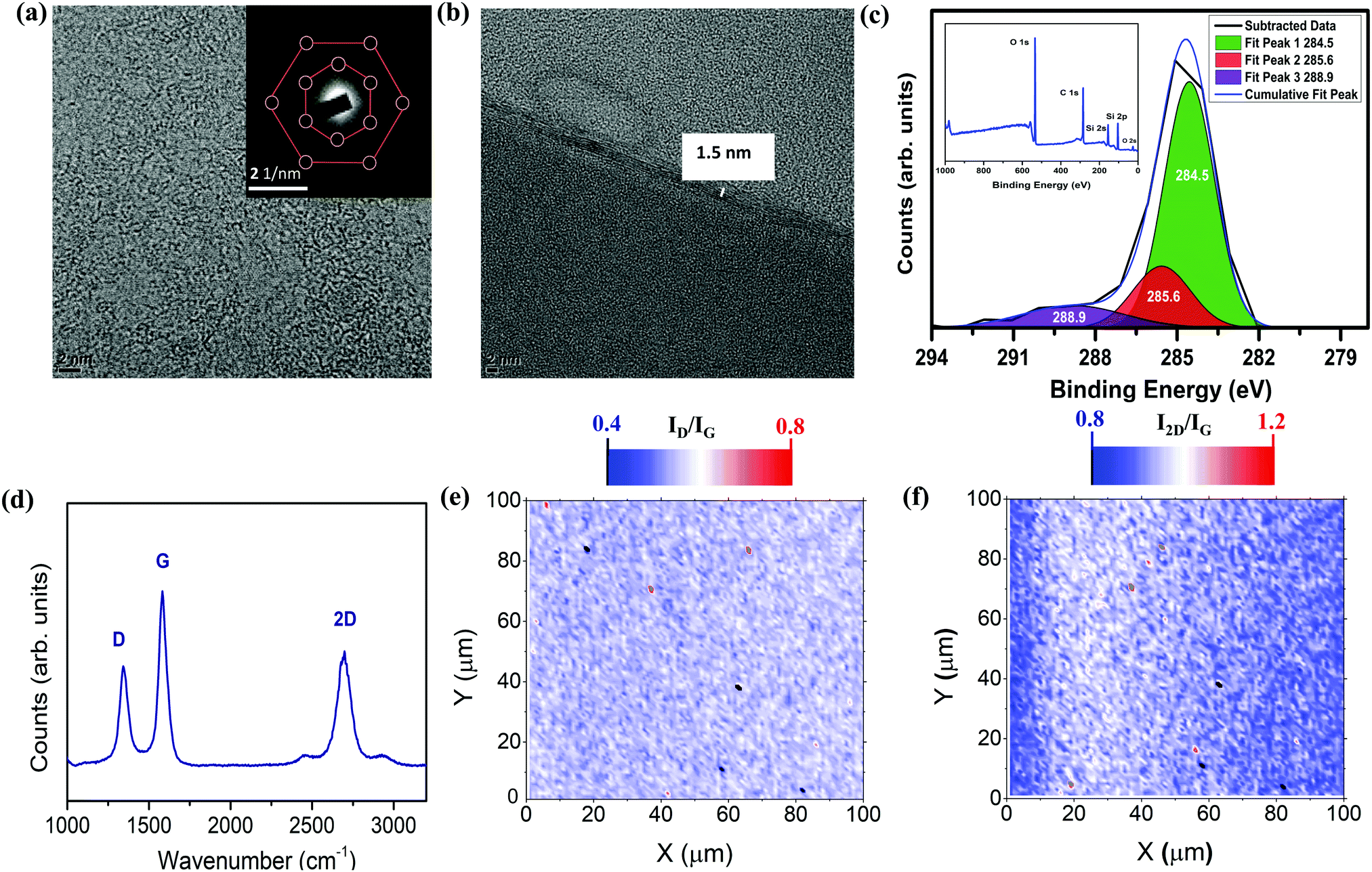 | ||
| Fig. 1 Graphene synthesis and characterization. (a) Transmission electron microscopy (TEM) image of the basal plane of graphene. The inset shows the selected area electron diffraction pattern. (b) Cross sectional TEM image with a graphene thickness of 1.5 nm (∼4L). (c) C 1s X-ray photoelectron spectroscopic data (de-convoluted) taken on graphene. The inset shows the survey spectrum. (d) Raman spectrum of 4L graphene (D, G and 2D peaks and the corresponding ratios are labelled). (e and f) ID/IG and I2D/IG intensity ratio maps acquired on a 100 μm × 100 μm area (ID, IG and I2D are intensities corresponding to D, G and 2D Raman peaks, respectively). | ||
The Raman spectrum shown in Fig. 1d clearly indicates the signature of FLG with finite disorder density evident as the D peak. The intensity ratio of Raman G (IG) and D peaks (ID) falls around 0.60, which indicates moderate disorder in the graphene sample. Fig. 1(e and f) show Raman maps for intensity ratios i.e. ID/IG and I2D/IG. The ID/IG map clearly indicates the uniform distribution of disorders in the 100 μm × 100 μm area. However, I2D/IG ≤1 in most of the regions indicates uniform growth of few layer graphene all over the mapped region. The estimated defect density nD and average distance between defects LD in our graphene devices are 1.8 × 1011 cm−2 and 14 nm respectively (details in the ESI†).
After characterizing the graphene layers, we carried out transport measurements on Hall bar devices in the geometry as shown in Fig. 2a. Fig. 2b shows longitudinal resistance (Rxx) as a function of back gate (VG) at various temperatures in the range of 6.5 K < T < 250 K. The position of the charge neutral point (CNP) in the positive VG regime is an indication of p-doped graphene layers. Two observations could be made from these temperature dependent data, (i) the value of the maximum resistivity increases at low temperature and (ii) the CNP shifts to higher positive VG at low temperature. Both of these observations have close resemblance to the characteristics reported for dual gated few bi-/trilayer graphene devices where a finite vertical displacement field leads to symmetry breaking,11 leading to the CNP shift and opening of an energy bandgap. Fig. 2c shows the Arrhenius plot for minimum conductivity values as a function of temperature, expressed as ln![[thin space (1/6-em)]](https://www.rsc.org/images/entities/char_2009.gif) σ = Φ/(kBT) where Φ and kBT are the thermal activation energy and Boltzmann constant, respectively. The activation energy in the FLG device corresponds to an energy bandgap which comes out to be 4.6 meV. Such an intrinsic bandgap in directly grown (on the SiO2/Si substrate) FLG is attributed to the substrate effect, which could be reconciled with a recent theoretical report where it has been predicted that the substrate-induced potential can break the honeycomb lattice symmetry and generate an energy bandgap.12
σ = Φ/(kBT) where Φ and kBT are the thermal activation energy and Boltzmann constant, respectively. The activation energy in the FLG device corresponds to an energy bandgap which comes out to be 4.6 meV. Such an intrinsic bandgap in directly grown (on the SiO2/Si substrate) FLG is attributed to the substrate effect, which could be reconciled with a recent theoretical report where it has been predicted that the substrate-induced potential can break the honeycomb lattice symmetry and generate an energy bandgap.12
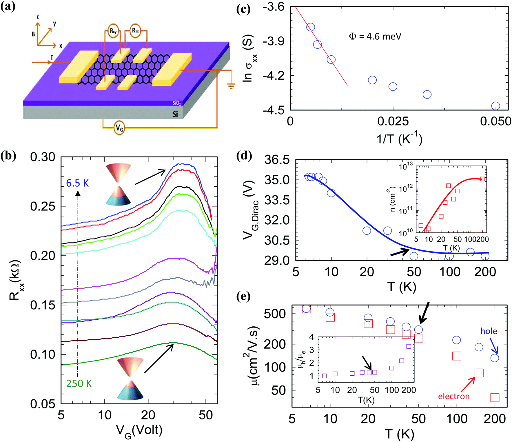 | ||
| Fig. 2 Temperature dependent transport measurements and electron–hole conduction asymmetry. (a) Optical image of the measured device with contact details. (b) Gate dependent longitudinal resistance measured in the temperature range as labelled. The insets show the schematic illustration of the Fermi level position at 250 K and 6.5 K. (c) Arrhenius plot taken from temperature dependence of minimum conductivity points from panel (b). Estimated thermal activation energy is ∼4.6 meV. (d) Shift in resistivity peaks (Dirac point) as a function of temperature. A sharp increase in gate bias corresponding to Dirac points below 4.6 meV (53 K) can be seen (arrow indicates T = 53 K). The inset shows the temperature dependence of Hall electron density expressed as n = −1/e × dRxy/dB. (e) Temperature dependent hole (μh)/electron (μe) mobilities with evident asymmetry beyond T = 53 K (4.6 meV). The inset shows temperature dependent evolution of the magnitude of the mobility ratio (μh/μe). | ||
The shift of the CNP with temperature is quantitatively summarized in Fig. 2d. The shift clearly indicates the increased p-doping in few-layer graphene at low temperature. This observation is also supported by reduced electron Hall density, n, at low temperatures as shown in the inset of Fig. 2d. Interestingly, the CNP and n both remain temperature independent in the range of 53 K < T < 250 K and a substantial increase (decrease) in CNP (n) starts below 53 K (∼4.6 meV). As soon as the thermal energy is reduced below 4.6 meV, the effect of the energy bandgap comes into picture, which manifests the effect of the energy bandgap (4.6 meV) on current-transport in our devices. A significant impact of thermally activated transport below T = 53 K is not only limited to the CNP shift and reduction in n, but also leads to the temperature dependent electron–hole conduction asymmetry,13 which is manifested as the deviation of hole and electron mobilities (μh and μe, respectively) from μh/μe = 1. Fig. 2e summarizes temperature dependent hole and electron mobilities determined from Hall measurements. Tenfold enhancement in the electron mobility of ∼600 cm2 V s−1 at 6.5 K indicates phonon dominated transport and good quality of directly grown FLG on SiO2/Si substrates. Interestingly, there is a small conduction asymmetry, i.e. μh/μe ∼1.25, below T = 53 K. However, at T >53 K, conduction asymmetry diverges and reaches up to 3.3. Beyond T = 53 K, the conduction asymmetry evolves as μh/μe ∝ T0.6. Such a striking difference in asymmetry below and above the energy bandgap could be qualitatively understood in the framework of relativistic/non-relativistic carriers.13
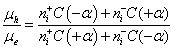
At T >53 K, carriers will have enough thermal energy to overcome the energy bandgap. Hence, in the range of 53 K < T < 250 K, FLG will behave more like a gapless semiconductor which facilitates relativistic Fermi velocity due to unique band dispersion. In this view, current-transport will be explained in the framework of the relativistic nature of carriers in FLG. In recent experimental and theoretical reports, it has been established that in contrast to a non-relativistic quantum system, the scattering cross section in a relativistic quantum system does depend on the sign of scattering potential and could be expressed as13,14
 | (1) |
Here, α is the impurity strength, and n+i, n−i are the positive and negative impurity density, respectively. Hence, in the framework of the relativistic system, electrons will be scattered off strongly as compared to holes from a donor impurity. This is consistent with μh/μe > 1 as observed in our devices at T > 53 K. However, at T < 53 K, the thermal energy will be smaller as compared to the energy band gap. Due to lack of the thermal activation of carriers below 50 K, it leads to two orders of magnitude decrease in electron density at 6.5 K as shown in Fig. 2d. Such a reduction in carrier density would naturally lead to strong suppression in e−–e− interactions and charge impurity scattering. This is also reflected in magneto-transport measurements where enhancement in coherence length at low temperature is observed (will be discussed later). As a consequence, conduction asymmetry, which occurs due to the scattering of relativistic carriers via charged impurities, will be suppressed. This qualitatively explains the temperature dependent electron–hole conduction asymmetry in our devices.
As discussed before, the presence of a Raman D peak indicates structural disorder in FLG directly grown onto SiO2/Si substrates. To understand more about intrinsic disorder and its impact on device features, we carried out temperature dependent magneto-transport measurements. Magneto-conductance, σxx (B), is measured in the temperature range of 6.5 K < T < 200 K. Fig. 3a shows normalized magneto-conductance, Δσxx = σxx (B) − σxx (0), plotted against perpendicular magnetic field, B. Strong suppression of the Δσxx with magnetic field is a robust signature of the WL in our devices. This manifests that the electron weak localization originates from the constructive interference of backscattered electron wave functions which gets suppressed upon applying a perpendicular magnetic field because of the phase shift in the wave function and is consistent with the established theory and already reported results.15–17
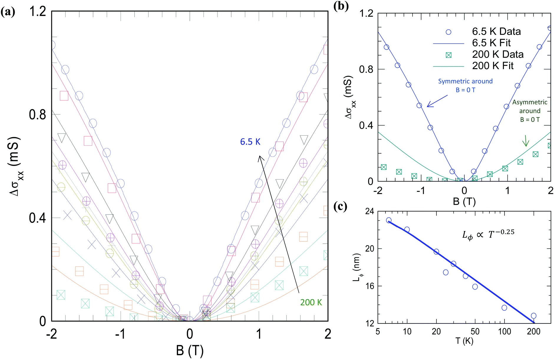 | ||
| Fig. 3 Observation of weak localization. (a) Δσxx = σxx(B) − σxx(0) plotted as a function of perpendicular magnetic field for various temperatures in the range of 6.5 K < T < 200 K. Symbols are the data points and solid lines are fit according to the HLN model (see the text). The inset shows fitting of the data taken at T = 6.5 K and 200 K. (b) Coherence length (Lϕ) estimated from HLN fitting of the magneto conductance data as shown in the panel (a). Temperature dependence of Lϕ exhibits power law, Lϕ ∝ T−0.25. Symbols are the data points and solid lines are guide to eyes. | ||
Remarkably, WL in our devices sustains till higher temperatures (T >200 K), which could be attributed to the thickness of the graphene (4L). In FLG, mesoscopic corrugations, which can cause a dephasing effect (equivalent to an internal magnetic field), are substantially suppressed and inter-valley scattering is enhanced. It leads to the observed enhancement of positive conductance, resulting in the restoration of the weak localization up to relatively higher temperature.18–20 In order to explain the observed behaviour, we model our data with the established modified HLN model for weak localization,15 which is expressed as
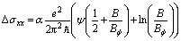 | (2) |
 ,ψ is the digamma function; Lϕ, the coherence length; e, the electronic charge; ℏ, the reduced Planck's constant; and β, the empirical fitting parameter. Fitting to the data allows us to extract the characteristic length (Lϕ) which is the dephasing length of the electrons. Fig. 3b shows the characteristic length extracted from the fits and plotted for varying temperature. Lϕ increases with decreasing temperature and reaches up to 27 nm at 6.5 K. Temperature dependence of Lϕ exhibits power law behaviour Lϕ ∝T−0.25 which is consistent with previous reports for two dimensional electron gas.21,22 The extracted Lϕ is less than the sample size (5 μm) to a great extent. This indicates the fact that the dominating factor of the scattering is not the edges but rather the defects and disorders present in the sample occurring during the growth process.23–26 The possible defects could be the adatoms such as hydrogen impurities inevitable during the atmospheric pressure thermal CVD growth of graphene (also appeared in XPS results).
We note that magneto-transport data show good agreement with the HLN model at low temperatures. However, at T >50 K, magneto-transport data could not be fully reproduced using the HLN model and fitting curves deviate from the recorded data (inset: Fig. 3a). This deviation comes with the evident asymmetry in magneto-conductance around B = 0 T that appears at higher temperatures. The exact origin of this temperature dependent asymmetry in the magneto-conductance is not precisely understood and requires further experimental investigation.
It is worthwhile to discuss that weak localization requires disorder in the device channel. However, in substantially disordered graphene devices, mobility should be limited by charged impurity scattering rather than due to phonons. Hence, the coexistence of WL and phonon limited mobility (Fig. 2e) is striking due to contrasting origins of these phenomena. In a work done by I. Childres et al.,27 a similar effect in graphene devices has been reported where WL (requires disorder) and the quantum Hall effect (occurs in clean devices) were simultaneously observed. However, in a separate work by Y. Du et al.,28 and Y. Shi et al.,29 on black phosphorus, it is clearly demonstrated that in the regime where WL exists, carrier mobility is primarily limited due to defect scattering, i.e. mobility remains temperature independent. In this view, we believe that concurrence of WL and phonon limited mobility has been possible due to low disorder in directly grown graphene. This is also reflected in Hall carrier density values (1010 cm−2–1012 cm−2) measured in our devices.
Conclusions
In conclusion, we carried out temperature dependent electrical/magneto-transport measurements on devices based on FLG grown directly on SiO2 surfaces via CVD. The measured devices exhibit an intrinsic energy band-gap of 4.6 meV which causes temperature dependent electron–hole conduction asymmetry. WL and phonon limited carrier mobility have contrasting sources of origin, hence, observation of these two competing phenomena together in our devices clearly indicates the low disorder in directly grown few layer graphene. This has been verified using Raman mapping and an electron mobility of up to 600 cm2 Vs−1 at low temperatures. We anticipate that large area graphene layers with high quality directly grown on an insulator could provide a good platform for graphene based large scale electronics.Author contributions
M. S. A. performed graphene growth. M. S. A. fabricated devices with the help taken from Y. H. M. S. A and P. K. S. performed electrical and magneto transport measurements, analysed data and cowrote the manuscript. C. L. supervised the project. All authors discussed and commented on the manuscript.Conflicts of interest
The authors declare no conflict of interest.Acknowledgements
This research was supported by the Basic Science Research Program through the National Research Foundation of Korea (2016K1A1A2912707, 2020R1A2C2014687, and 2021R1I1A1A01050054), funded by the Ministry of Science and ICT of Korea, Samsung Research Funding Centre of Samsung Electronics (project no. SRFC-TB1803-04).Notes and references
- K. I. Bolotin, K. J. Sikes, Z. Jiang, M. Klima, G. Fudenberg, J. Hone, P. Kim and H. L. Stormer, Ultrahigh electron mobility in suspended graphene, Solid State Commun., 2008, 146, 351–355 CrossRef CAS.
- L. Banszerus, M. Schmitz, S. Engels, J. Dauber, M. Oellers, F. Haupt, K. Watanabe, T. Taniguchi, B. Beschoten and C. Stampfer, Ultrahigh-mobility graphene devices from chemical vapor deposition on reusable copper, Sci. Adv., 2015, 1, e1500222 CrossRef PubMed.
- C. Lee, X. Wei, J. W. Kysar and J. Hone, Measurement of the elastic properties and intrinsic strength of monolayer graphene, Science, 2008, 321, 385–388 CrossRef CAS PubMed.
- X. Du, I. Skachko, A. Barker and E. Y. Andrei, Approaching ballistic transport in suspended graphene, Nat. Nanotechnol., 2008, 3, 491–495 CrossRef CAS PubMed.
- M. Yi and Z. Shen, J. Mater. Chem. A, 2015, 3, 11700–11715 RSC.
- N. Petrone, C. R. Dean, I. Meric, A. M. van der Zande, P. Y. Huang, L. Wang, D. Muller, K. L. Shepard and J. Hone, Chemical vapor deposition-derived graphene with electrical performance of exfoliated graphene, Nano Lett., 2012, 12, 2751–2756 CrossRef CAS PubMed.
- A. Reina, X. Jia, J. Ho, D. Nezich, H. Son, V. Bulovic, M. S. Dresselhaus and K. Jing, Large area, few-layer graphene films on arbitrary substrates by chemical vapor deposition, Nano Lett., 2009, 9, 30–35 CrossRef CAS PubMed.
- N. Mishra, S. Forti, F. Fabbri, L. Martini, C. McAleese, B. R. Conran, P. R. Whelan, A. Shivayogimath, B. S. Jessen, L. Buß, J. Falta, I. Aliaj, S. Roddaro, J. I. Flege, P. Bøggild, K. B. K. Teo and C. Coletti, Wafer-Scale Synthesis of Graphene on Sapphire: Toward Fab-Compatible Graphene, Small, 2019, 15, 1904906 CrossRef CAS PubMed.
- C. Y. Dai, W. C. Wang, C. A. Tseng, F. C. Ding, Y. T. Chen and C. C. Chen, Spatial Confinement Approach Using Ni to Modulate Local Carbon Supply for the Growth of Uniform Transfer-Free Graphene Monolayers, J. Phys. Chem. C, 2020, 124, 23094–23105 CrossRef CAS.
- Y. Ueda, T. Maruyama and S. Naritsuka, Effect of Growth Pressure on Graphene Direct Growth on an A-Plane Sapphire Substrate: Implications for Graphene-Based Electronic Devices, ACS Appl. Nano Mater., 2021, 4, 343–351 CrossRef CAS.
- W. Zhao, B. Xia, L. Lin, X. Xiao, P. Liu, X. Lin, H. Peng, Y. Zhu, R. Yu, P. Lei, J. Wang, L. Zhang, Y. Xu, M. Zhao, L. Peng, Q. Li, W. Duan, Z. Liu, S. Fan and K. Jiang, Low-energy transmission electron diffraction and imaging of large-area graphene, 2017 Search PubMed.
- A. Kovtun, D. Jones, S. Dell’Elce, E. Treossi, A. Liscio and V. Palermo, Accurate chemical analysis of oxygenated graphene-based materials using X-ray photoelectron spectroscopy, Carbon, 2019, 143, 268–275 CrossRef CAS.
- Y. Lee, D. Tran, K. Myhro, J. Velasco, N. Gillgren, C. N. Lau, Y. Barlas, J. M. Poumirol, D. Smirnov and F. Guinea, Competition between spontaneous symmetry breaking and single-particle gaps in trilayer graphene, Nat. Commun., 2014, 5, 1–5 Search PubMed.
- S. Sahu and G. C. Rout, Band gap opening in graphene: a short theoretical study, Int. Nano Lett., 2017, 7, 81–89 CrossRef CAS.
- P. K. Srivastava, S. Arya, S. Kumar and S. Ghosh, Relativistic nature of carriers: Origin of electron-hole conduction asymmetry in monolayer graphene, Phys. Rev. B, 2017, 96, 241407 CrossRef.
- D. S. Novikov, Cite as, Appl. Phys. Lett., 2007, 91, 102102 CrossRef.
- E. Mccann, K. Kechedzhi, V. I. Fala’Ko, H. Suzuura, T. Ando and B. L. Altshuler, Weak-localization magnetoresistance and valley symmetry in graphene, Phys. Rev. Lett., 2006, 97, 146805 CrossRef CAS PubMed.
- V. I. Fal’ko, K. Kechedzhi, E. McCann, B. L. Altshuler, H. Suzuura and T. Ando, Weak localization in graphene, Solid State Commun., 2007, 143, 33–38 CrossRef.
- X. Wu, X. Li, Z. Song, C. Berger and W. A. de Heer, Weak antilocalization in epitaxial graphene: Evidence for chiral electrons, Phys. Rev. Lett., 2007, 98, 136801 CrossRef PubMed.
- W. Wang, L. Chen, Z. Wang, Y. Wang, T. Li and Y. Wang, Weak localization in few-layer graphene grown on copper foils by chemical vapor deposition, Carbon, 2012, 50, 5242–5246 CrossRef CAS.
- H. Cao, Q. Yu, L. A. Jauregui, J. Tian, W. Wu, Z. Liu, R. Jalilian, D. K. Benjamin, Z. Jiang, J. Bao, S. S. Pei and Y. P. Chen, Electronic transport in chemical vapor deposited graphene synthesized on Cu: Quantum Hall effect and weak localization, Appl. Phys. Lett., 2010, 96, 122106 CrossRef.
- R. S. Gonnelli, E. Piatti, A. Sola, M. Tortello, F. Dolcini, S. Galasso, J. R. Nair, C. Gerbaldi, E. Cappelluti, M. Bruna and A. C. Ferrari, Weak localization in Electric-double-layer gated Few-layer graphene, 2D Mater., 2017, 4, 035006 CrossRef.
- J. Appenzeller, R. Martel, P. Avouris, H. Stahl, U. T. Hunger and B. Lengeler, Phase-coherent transport in ropes of single-wall carbon nanotubes, Phys. Rev. B: Condens. Matter Mater. Phys., 2001, 64, 121404 CrossRef.
- S. Minke, J. Bundesmann, D. Weiss and J. Eroms, Phase coherent transport in graphene nanoribbons and graphene nanoribbon arrays, Phys. Rev. B: Condens. Matter Mater. Phys., 2012, 86, 155403 CrossRef.
- F. v. Tikhonenko, D. W. Horsell, R. v. Gorbachev and A. K. Savchenko, Weak localization in graphene flakes, Phys. Rev. Lett., 2008, 100, 056802 CrossRef CAS PubMed.
- T. H. Bointon, I. Khrapach, R. Yakimova, A. V. Shytov, M. F. Craciun and S. Russo, Approaching magnetic ordering in graphene materials by FeCl3 intercalation, Nano Lett., 2014, 14, 1751–1755 CrossRef CAS PubMed.
- I. Childres, L. A. Jauregui, J. Tian and Y. P. Chen, Effect of oxygen plasma etching on graphene studied using Raman spectroscopy and electronic transport measurements, New J. Phys., 2011, 13, 025008 CrossRef.
- Y. Du, A. T. Neal, H. Zhou and P. D. Ye, Weak localization in few-layer black phosphorus, 2D Mater., 2016, 3, 024003 CrossRef.
- Y. Shi, N. Gillgren, T. Espiritu, S. Tran, J. Yang, K. Watanabe, T. Taniguchi and C. N. Lau, Weak localization and electron-electron interactions in few layer black phosphorus devices, 2D Mater., 2016, 3, 034003 CrossRef.
Footnote |
| † Electronic supplementary information (ESI) available. See DOI: 10.1039/d1cp03225a |
| This journal is © the Owner Societies 2021 |