
Soft skin layers for reconfigurable and programmable nanowrinkles
Dongjoon
Rhee
 a,
Shikai
Deng
b and
Teri W.
Odom
*ab
a,
Shikai
Deng
b and
Teri W.
Odom
*ab
aDepartment of Materials Science and Engineering, Northwestern University, Evanston, Illinois 60208, USA. E-mail: todom@northwestern.edu
bDepartment of Chemistry, Northwestern University, Evanston, Illinois 60208, USA
First published on 26th November 2020
Abstract
Wrinkling skin layers on pre-strained polymer sheets has drawn significant interest as a method to create reconfigurable surface patterns. Compared to widely studied metal or silica films, softer polymer skins are more tolerant to crack formation when the surface topography is tuned under applied strain. This Mini-review discusses recent progress in mechano-responsive wrinkles based on polymer skin materials. Control over the skin thickness with nanometer accuracy allows for tuning of the wrinkle wavelength and orientation over length scales from nanometer to micrometer regimes. Furthermore, soft skin layers enable texturing of two-dimensional electronic materials with programmable feature sizes and structural hierarchy because of the conformal adhesion to the substrates. Soft skin systems open prospects to tailor a range of surface properties via external stimuli important for applications such as smart windows, microfluidics, and nanoelectronics.
 Dongjoon Rhee | Dongjoon Rhee is a Ph.D. candidate in Materials Science and Engineering under supervision of Professor Teri W. Odom at Northwestern University. He received his B.S. and M.S. degrees in Materials Science and Engineering from Hanyang University, South Korea, in 2013 and from Northwestern University in 2016. His research focuses on multiscale patterning based on controlled surface wrinkling instabilities. |
 Shikai Deng | Dr. Shikai Deng is a postdoctoral fellow awarded a Cottrell Fellowship at Northwestern University. His research interest is designing multiscale metamaterials with unprecedented properties based on nanostructured surfaces and plasmonic core–shell nanoparticle lattices. He received his Ph.D. in Chemical Engineering at the University of Illinois at Chicago in 2017, where he worked on thin-film mechanics, nanowrinkles, and new electronic devices of 2D materials. Before that, he also received his B.S. in Chemical Engineering from Beijing University of Chemical Technology in 2012. |
 Teri W. Odom | Teri W. Odom is Charles E. and Emma H. Morrison Professor and Department Chair of Chemistry at Northwestern University. She is an expert in designing structured nanoscale materials that exhibit extraordinary size and shape-dependent optical and physical properties. Odom has pioneered a suite of multi-scale nanofabrication tools that have resulted in plasmon-based nanoscale lasers that exhibit tunable color, flat optics that can manipulate light, and hierarchical substrates that show controlled wetting and super-hydrophobicity. She has also invented a class of biological nanoconstructs that are facilitating unique insight into nanoparticle-cell interactions. |
1. Introduction
Reconfigurable surface patterns are topographical features that can change dimension and orientation in response to external stimuli.1,2 These structures support physical and chemical properties that can be reversibly tuned, which are beneficial for applications in smart windows, sensors, and actuators.3–5 Most work on creating responsive systems has focused on combining three-dimensional (3D) structures with deformable soft materials.6,7 For example, arrays of gold-coated epoxy microplates partially embedded into hydrogels can switch between upright (transparent) and tilted (opaque) states when the matrix swells or contracts under environmental changes.3 Also, elastomer nanopillar arrays can transition from a closer spaced (blue diffractive color) to a wider spaced configuration (red diffractive color) under tensile strain applied to the substrate.8 The length scales of surface patterns are critical for engineering a functional response; microscale features are typically used to tune surface adhesion and antibiofouling properties,9,10 and nanotextures are advantageous to tailor hydrophobicity/hydrophilicity and structural color.11,12 Because control over the periodicity and orientation of nano- and micrometer-sized patterns is needed for targeted properties, most reconfigurable surface structures require complex lithographic processes with multiple steps of masking and etching.Mechanical instabilities that result from the compression of a stiff thin material—often referred to as a skin layer—on a pre-strained polymer substrate have emerged as an approach to create surface textures over multiple length scales.13 Among different types of strain-induced patterns, wrinkles with sinusoidal shapes have been widely investigated.14,15 Wrinkle wavelength (λ) and amplitude (A) can be designed based on the materials properties of the system and applied strain, where λ ∼ 2πh(ES/3EB)1/3 and  , and h is the skin thickness, ES and EB are the Young's moduli of the skin and substrate, and ε is compressive strain that results from releasing a pre-strain (εpre).16,17 Wrinkle orientation can be controlled based on the direction of strain;18 uniaxial strain relief results in highly aligned wrinkles in a single direction, while biaxial strain relief produces two-dimensional (2D) wrinkles with quasi-random orientations. Because wrinkle wavelength, amplitude, and orientation can be tuned in response to the substrate strain, reversible modification of properties is possible by applying external stimuli.19,20
Conventional stimuli-responsive wrinkles are based on a bi-layer architecture of elastomer substrates (such as poly(dimethylsiloxane), PDMS) coated with skin layers formed by deposition of a thin metal film or conversion of the surface into silica by an oxygen-plasma treatment.21–24 However, cracks form at random locations in the skin layers under tensile strain exceeding 10%,21,25 which hinders tuning of directional properties such as anisotropic water spreading and light diffraction.19,26 Mechanical instabilities can also result in delamination of the skin layer when the wrinkle topography is changed under substrate stretching.19,21 Although the wrinkle wavelength in these bi-layer systems can be controlled at the microscale, nanowrinkles are difficult to achieve because the Young's modulus of the skin (typically 40–280 GPa)21–24 is much larger than the substrate (0.5–4 MPa).27
Crack formation in wrinkled substrates can be suppressed by using soft polymer skin layers.28–33 Most efforts have been based on polymer thin films created by solution processing techniques that can generate crack-free wrinkles with wavelengths ranging from hundreds of nanometers to tens of micrometers.28–31 Systematic design of nanoscale features using solution-based methods, however, is challenging because of limited control over the skin thickness. Recently, fluorine-based plasma deposition on elastomeric or thermoplastic sheets can produce fluoropolymer skin layers with nm-scale tunable thickness, which allows the wrinkle wavelength to be tailored from several micrometers down to tens of nanometers.32 Because plasma-deposited skin layers are conformal to the underlying substrate and do not delaminate,33,34 switching wrinkle orientation or introducing hierarchical structures is possible by accessing high strain regimes (ε > 0.6).33–35
This Mini-review discusses advances in reconfigurable wrinkles enabled by soft skin layers. First, we review solution processing techniques that can form polymer skin materials. Compared to conventional systems based on stiffer skin layers, cracking is greatly suppressed when the wrinkle orientation is switched under tensile strain. We then introduce plasma processes that can access accurate thicknesses of the soft skin layers needed to control the wrinkle wavelength both in nano- and micrometer regimes. Finally, we describe how soft skin layers can be used to pattern thin functional materials such as graphene and other 2D nanomaterials with customizable feature sizes and structural hierarchy.
2. Solution-processed polymer skin layers
In general, a skin/substrate bilayer system can accommodate more tensile strain without crack formation when the modulus ratio ES/EB is small.36 Polymer skin layers with Young's moduli ranging from hundreds of MPa to several GPa (ES/EB < 5000)29,30,33,37,38 are advantageous for fabricating crack-free wrinkles compared with metal or silica (ES/EB ranging from 2.4 × 10⁴ to 1.8 × 10⁵).21–24 The most common method to produce soft skin layers is by drop casting polymer solutions such as poly(vinyl alcohol) (PVA).28,29 Depositing PVA on a pre-strained PDMS slab followed by solvent evaporation results in films with an average thickness of a few micrometers.28,29 Upon strain relief, the PVA/PDMS system (ES/EB ≈ 1900) forms wrinkles (λ ≈40–110 μm; h ≈4–7 μm) that can be repeatedly switched between wrinkled and flat states up to high strain (εpre = 90%).28 This approach, however, cannot achieve uniform λ over centimeter-scale areas since the thickness of the skin layer is uneven because of coffee-ring features and aggregation after drying.39 The fabrication of wrinkles with sub-micrometer wavelengths is also difficult because the films tend to be thicker than one micron.28,29,40 Meniscus-guided coating techniques such as solution shearing and dip coating can also create polymer skin layers with controlled thickness;41,42 however, these strategies often result in discontinuous films for thicknesses <100 nm because the solution meniscus pins and de-pins during the coating process.43In contrast, spin coating can produce continuous skin layers with a uniform thickness ranging from tens to hundreds of nanometers (Fig. 1).30,31,37,44,45 This technique has been used to process a range of polymers on pre-strained elastomer substrates and to generate wrinkles for stretchable electronics (Fig. 1a). For example, a composite organic semiconductor spin-cast on a pre-strained (εpre = 20%) PDMS substrate (ES/EB ≈800–4100) formed microscale wrinkles (λ ≈10 μm) upon strain relief that could be stretched without cracking up to the pre-strain amount (Fig. 1b).30 As a result, the photovoltaic properties of the wrinkled composite were nearly identical after stretch-release cycles. Although spin coating can control the length scale of features by varying h, this method is limited because (1) defects such as voids and striation patterns result in skin layers that are not uniform in thickness, especially for h < 20 nm, and thus controlling topography for sub-200 nm wrinkles is difficult;31,46 and (2) oxygen plasma treatment used to improve wetting of the precursor solution can form brittle silica films that result in cracking in the skin layer when the substrate is stretched more than 10%.47
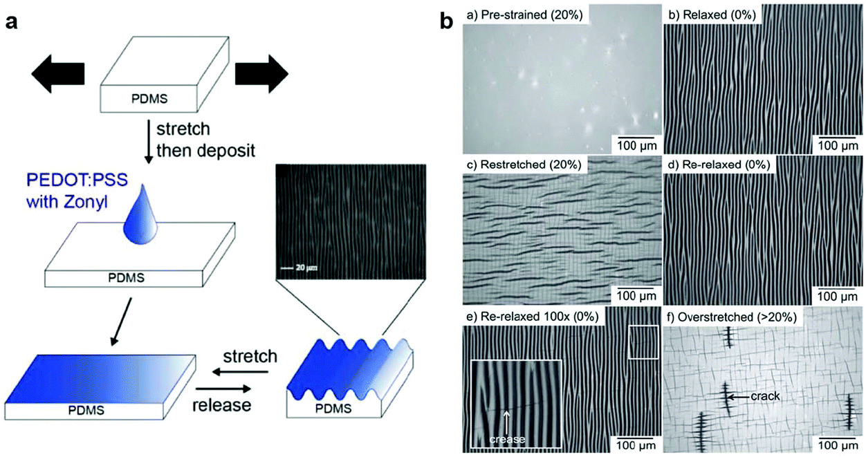 | ||
| Fig. 1 Mechano-responsive patterns from wrinkling solution-processed polymer skin layers. (a) Fabrication of polymer wrinkles based on spin-coating. (b) Structural evolution of wrinkled organic semiconductor film at different strains. Panel a adapted with permission from ref. 37. Copyright 2019 John Wiley and Sons. Panel b adapted with permission from ref. 30. Copyright 2011 John Wiley and Sons. | ||
3. Monolithic polymer skin layers from chemical vapor deposition
Chemical vapor deposition (CVD) can also form soft skin layers of organic semiconductors as well as fluoropolymers conformally coated on pre-strained substrates.48,49 CVD polymers are commonly synthesized based on free radical chain growth or oxidative step growth.48,49 For both mechanisms, vapor-phase monomers are delivered to the substrate and then activated by initiators or oxidizing agents to produce polymer chains. Because the CVD process does not rely on solution processing, ultra-thin (<10 nm) skin layers can be created without needing the surface to be hydrophilic, which is typically realized by applying an oxygen plasma.48–50 Mechanically robust, fluoropolymer (CFx) layers from CHF3 plasma treatment have recently formed wrinkles on various substrates including elastomers and thermoplastics.32,33 The plasma process generates fluorine-containing chemical species that polymerize into a CFx film composed of multiple bonding components: C–Fx (x = 1–3), C–C, and C–CFx crosslinks.33,51 The thickness of the CFx skin can be controlled from sub-10 nm to hundreds of nm with nanometer precision, which enables continuous tuning of the resulting λ from tens of nanometers to several micrometers.32,33Wrinkles on elastomer substrates can be tuned by mechanical stretching at room temperature (Fig. 2).19,22 Although the orientation of the microscale textures can be switched under a tensile strain greater than the pre-strain amount, cracks form in the silica skin layer (Esilica ≈40–76 GPa; Esilica/EPDMS ≈2.4 × 10⁴–3.8 × 10⁴) on PDMS.19,33 Silica films with Young's moduli comparable to those of polymer skin layers can be prepared by adjusting oxygen-plasma processing conditions;52 however, the skin/PDMS composite cannot be stretched >10% without crack formation because silica is brittle.53 CHF3-plasma-treated PDMS has emerged as a promising platform for realizing reconfigurable wrinkles because the CFx layer is softer (ECFx ≈1 GPa; ECFx/EPDMS ≈610) and more ductile than silica.33,54 The CFx skin/PDMS composite can achieve more than a 10-fold increase in uniaxial pre-strain relief without cracking and provides a wider range of tunability over λ and A by changing pre-strain in a crack-free regime (Fig. 2a). When the substrate is stretched more than the pre-strained amount, the wrinkles switch orientation perpendicular to their as-fabricated state and can return to the initial orientation upon release. Notably, cracking and delamination are suppressed in the CFx skin layer during the topographical transformation. Except for a slight decrease in the wrinkle amplitude after release from the first stretched state as a result of plastic deformation explained by modeling,33,55 the wrinkles exhibit nearly identical amplitude for subsequent stretching and releasing, up to 1000 times. In contrast, silica-skin wrinkles exhibit cracking and delamination when surface topography changes under tensile strain (Fig. 2b). Although the wrinkles can switch between an initial and switched orientation, wrinkles adjacent to cracks show a significant decrease in amplitude because cracks reduce compressive strain in the skin layer. The spatial uniformity in wrinkle amplitude continually decreases as more cracks form during repeated switching of wrinkle orientation.
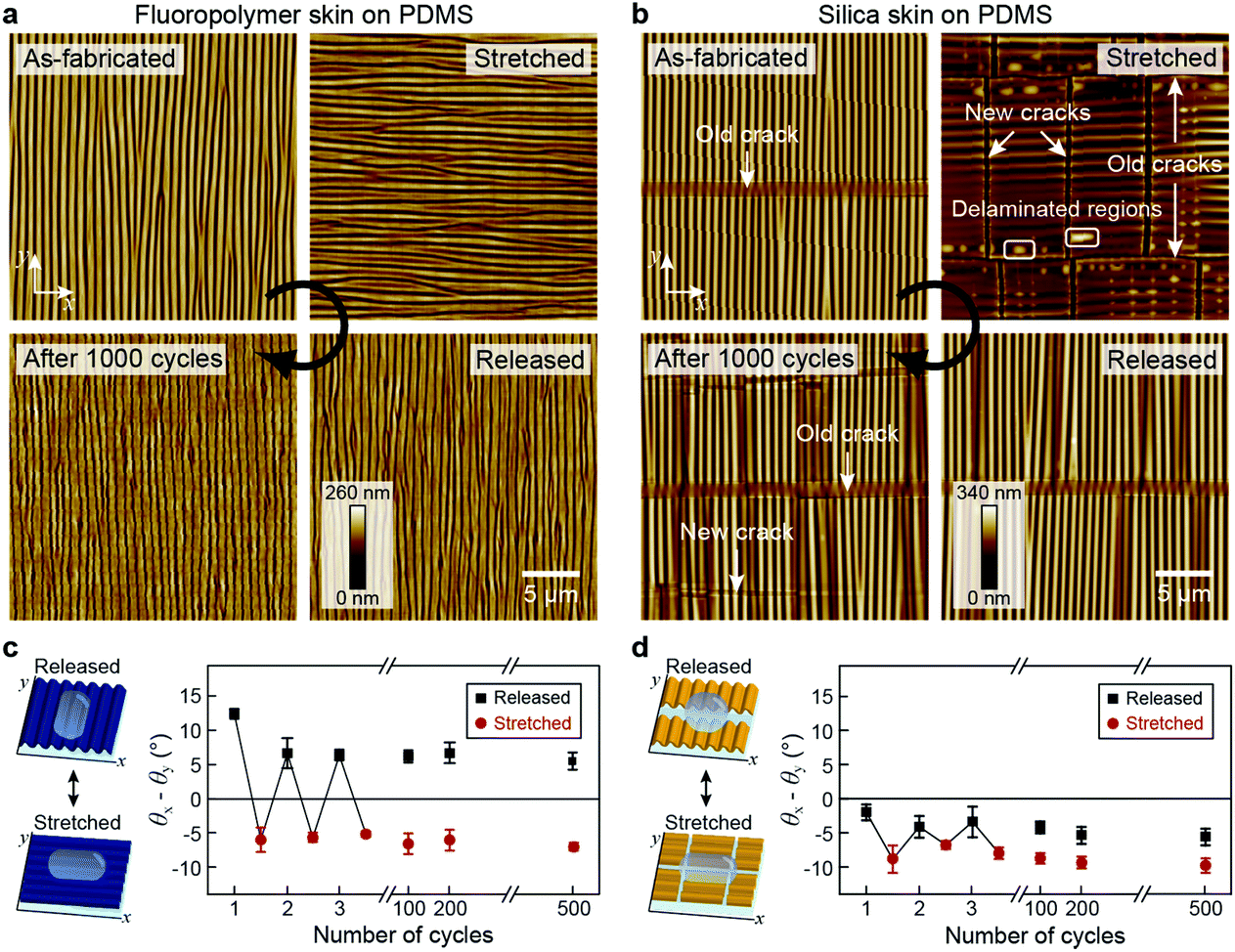 | ||
| Fig. 2 Crack-free nanowrinkles with switchable orientation enabled by plasma-mediated soft skin layers. Side-by-side comparison of wrinkle topography of (a) fluoropolymer and (b) silica skin wrinkles under stretch-release cycles. Anisotropic wetting on wrinkled (c) fluoropolymer and (d) silica skin layers. Adapted with permission from ref. 33. Copyright 2017 John Wiley and Sons. | ||
The wrinkled CFx layer on PDMS can control the direction of anisotropic water spreading when mechanical strain is applied to the system.33 Because water droplets preferentially spread along the wrinkle orientation, the surface can switch between positive and negative Δθ (where Δθ is the difference in water contact angle measured perpendicular and parallel to the initial wrinkle orientation) during stretch-release cycles (Fig. 2c). Silica-coated PDMS did not support this wetting behavior, and the bi-layer only exhibited negative Δθ for both initial and switched wrinkle orientations because the cracks hindered droplet spreading (Fig. 2d). With robust control over wrinkle orientation by external strain, crack-free CFx-skin-based wrinkles can be used in microfluidics and directional water collection systems.56–58
4. Composite skin layer: soft fluoropolymer and graphene
Texturing graphene has emerged as a means to engineer electronic and mechanical properties for stretchable electronics,59 photodetectors,60 and energy storage devices61 without damaging the atomic lattice.62 Graphene crumples formed by strain relief of elastomer sheets show electrical conductivity and light absorption that are reversibly changed by applying strain.63–65 The crumple pitch for single-layer graphene, however, is typically less than 100 nm because the feature size scales with the skin thickness.66 Moreover, graphene forms cracks under stretching in the areas not directly supported by the substrate, which limits the range of applied tensile strain to tune crumple topography.63,67,68Sandwiching a CFx skin layer between graphene and a polymer substrate can also suppress the delamination of graphene from the substrate during strain relief (Fig. 3a).55,66 The strong adhesion between graphene and the CFx layer is attributed to electrostatic interactions associated with hole doping in graphene.55,69 Changing the fluoropolymer layer thickness based on CHF3 plasma treatment has resulted in graphene wrinkles with wavelengths ranging from several microns to tens of nanometers.66 Because conformal contact between graphene and the CFx layer is robust at high tensile strain, the wrinkle topography can be tuned under repeated stretching and releasing without crack formation.55 Conformal wrinkling can be used to engineer the physical properties of graphene such as emissivity (ratio of thermal radiation emitted from the surface of a material to that from a blackbody) (Fig. 3b).70 Compared to flat graphene with a uniform and low emissivity (∼0.02) over a broad spectrum (0.1–20 μm),70,71 graphene wrinkles exhibit increased emissivity at wavelengths that scales with the feature size (hundreds of nm to tens of μm). Since graphene can be reversibly flattened or wrinkled, switching between low- and high-emissivity states is possible without a notable decrease in maximum emissivity values.
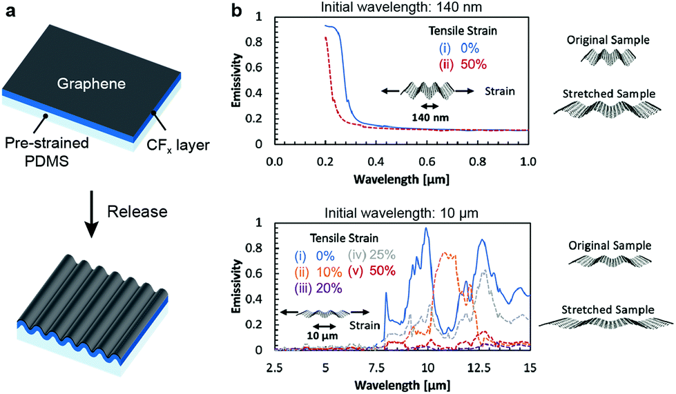 | ||
| Fig. 3 Conformal graphene wrinkles for tunable emissivity. (a) Scheme describing conformal wrinkling of graphene on fluoropolymer-coated PDMS. (b) Emissivity of nanotextured graphene with different feature sizes. Panel a adapted with permission from ref. 55. Copyright 2020 American Chemical Society. Panel b adapted with permission from ref. 70. Copyright 2019 American Chemical Society. | ||
Conformal wrinkling can realize multiscale structures with locally different feature sizes side-by-side on a single graphene sheet.55,66,72Fig. 4a shows textured graphene patterned with four microdomains with distinct wrinkle wavelengths. Prior to graphene transfer, CFx lines were first applied to the pre-strained PDMS substrate using area-selective skin growth.55 Another cycle of patterned CFx layer deposition and unmasked CHF3 plasma treatment resulted in four areas with different skin thicknesses (h1 ≈8 nm; h2 ≈14 nm; h3 ≈20 nm; h4 ≈27 nm). After graphene transfer followed by relief of the pre-strain (εpre = 30%), multiscale graphene wrinkles with four distinct wavelengths (λ1 ≈330 nm; λ2 ≈490 nm; λ3 ≈670 nm; λ4 ≈1000 nm) were formed because λ is proportional to h. In-plane hierarchical wrinkles switched orientations when the substrate was stretched to a tensile strain (60%) greater than the pre-strain amount and returned to the initial orientation upon release.55 Notably, the wrinkled graphene was mechanically robust and did not crack during switching of wrinkle orientations because conformal contact between graphene and the substrate was preserved even at boundaries between domains with different CFx thicknesses (Fig. 4a, zoomed-in images).
 | ||
| Fig. 4 Multiscale graphene wrinkles with spatially defined structural features and properties. (a) Graphene patterned with four regions with different wavelengths. (b) Spatially defined electrical conductivities after plasma functionalization. Panel a adapted with permission from ref. 55. Copyright 2020 American Chemical Society. Panel b adapted with permission from ref. 72. Copyright 2019 American Chemical Society. | ||
In addition, in-plane structural hierarchy enables the tailoring of the properties of graphene in an area-specific manner. Graphene substrates patterned with regions of different wrinkle wavelengths can show spatially defined fluorination levels after a single plasma reaction because the chemical reactivity of graphene scales with the local curvature (κ ∝ 1/λ) (Fig. 4b).72 Since electrical conductivity of graphene decreases with degree of fluorination, each domain on the functionalized graphene can show distinct current levels under conductive atomic force microscope images: the average current value increased by 10-fold by changing λ from 60 nm to 600 nm. Mechanical stiffness is another property that benefits from hierarchical nanowrinkling,66 where the peaks of the textured graphene show enhanced local stiffness by ∼560% when λ increased from 160 nm to 450 nm. Interestingly, the stiffness saturated when λ >400 nm, which highlights the importance of patterning nanoscale features for tuning the local properties of graphene.
5. Out-of-plane hierarchical structures from sequential wrinkling
The plasma-mediated deposition of the polymer skin layer ensures strong interfacial adhesion between the skin layer and substrate and enables access to high strain regimes (ε > 0.6) that can create complex hierarchical structures with controlled structural parameters.34,35 Sequential cycles of CFx skin growth followed by strain relief of a thermoplastic polystyrene (PS) sheet can produce 3D hierarchical wrinkles with characteristic generational (G) features (Fig. 5a).34 The process starts by treating a pre-strained PS substrate with the CHF3 plasma to form the first skin layer (h1). After relieving the strain (ε1) by heating the system above the glass transition temperature of PS (Tg = 100 °C), G1 wrinkles with the smallest wavelength (λ1) are created. G2 wrinkles with a larger wavelength (λ2) can form by depositing the second CHF3 plasma followed by a second strain relief (ε2) upon subsequent heating at a temperature higher than Tg. The process can be repeated until the desired structural hierarchy is achieved. Because adhesion between newly deposited CFx skin layers and the underlying wrinkle topography is maintained (Fig. 5b), the wavelengths and orientations of previous patterns are preserved when the next generation of features is added. For each sequential process, the system assumes wrinkle wavelengths that minimize the total energy required to deform the skin layers and substrate.73 The wavelength of the n-th generation wrinkles can be expressed as:where hn and εn are the skin thickness and strain relief amount for the n-th cycle.
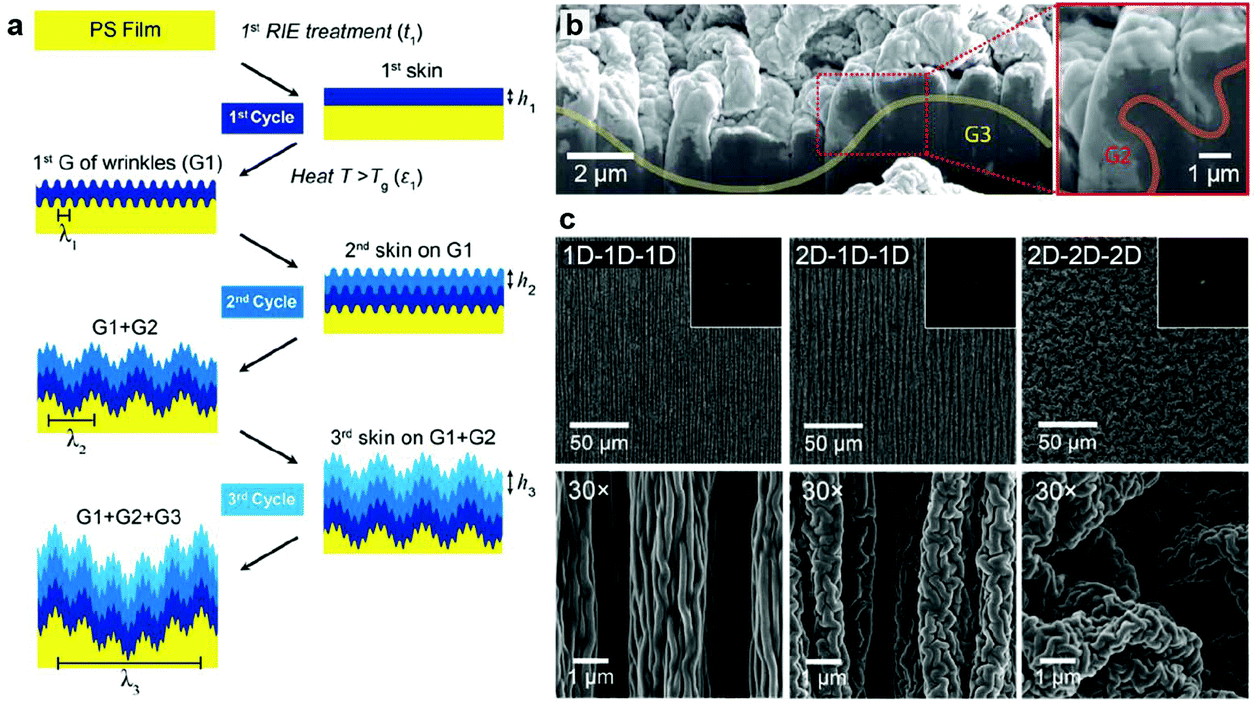 | ||
| Fig. 5 Multigenerational, hierarchical structures from sequential wrinkling of plasma-mediated soft skin layers. (a) Design principles of sequential process. (b) Conformal interface between skin layers and substrate. (c) Hierarchical wrinkles from three cycles of sequential skin growth and strain relief. Adapted with permission from ref. 34. Copyright 2015 American Chemical Society. | ||
Fig. 5c shows 3D hierarchical structures based on three-cycle G1–G2–G3 process with the same combination of CFx thicknesses (h1 ≈20 nm; h2 ≈100 nm; h3 ≈180 nm). The orientation of each G feature can be independently controlled by relieving strain in either a biaxial (2D) or uniaxial (1D) direction for each cycle, while the wrinkle wavelengths are roughly constant (λ1 ≈220 nm; λ2 ≈1 μm; λ3 ≈12 μm). Interestingly, G3 orientation was determined not only by the ε3 direction but also by the wrinkle orientations in G1–G2 patterns; relieving strain uniaxially for three times (1D–1D–1D) resulted in highly aligned G3 features while 2D–1D–1D cycle produced less ordered G3 wrinkles because of randomly-oriented G1 features. The most disordered G3 structures were obtained from the 2D–2D–2D process. By varying h and strain relief directions for each cycle, sequential wrinkling can fabricate hierarchical architectures with nearly unlimited combinations of λ and orientation.
Although sequential skin growth and strain relief can readily design 3D hierarchical structures in polymers, this approach has drawbacks for general skin materials because progressively thicker layers are needed to access higher G features. This thickness requirement may compromise the functionality of 2D electronic materials with thickness-dependent properties.74 To pattern multi-generational structures into a single layer of functional skin, sequential wrinkling with sacrificial skin layers has been developed (Fig. 6a).75 First, a 2D material is transferred onto a pre-strained PS substrate followed by strain relief to form G1 wrinkles with λ1. G2 wrinkles with λ2 are then generated by spin-coating a polyvinylpyrrolidone (PVP) skin layer with thickness h2 on the patterned surface followed by a second strain relief (ε2). The textured functional surface material is revealed after dissolving the PVP layer with ethanol. Cycles of PVP deposition, strain relief, and PVP dissolution can result in multi-G wrinkles with programmable structural hierarchy (e.g. n + 1 characteristic wavelengths after n cycles). The PVP-assisted sequential process has created G1–G2 wrinkles on MoS2 with enhanced catalytic activity for hydrogen evolution reaction by reducing adhesion of hydrogen bubbles. In addition to MoS2, this strategy can pattern various low-dimensional materials such as thin metal films, graphene, 2D semiconductors (e.g. WS2 and SnS2), and carbon nanotubes, which are advantageous for applications in photonics and electrocatalysts (Fig. 6b).
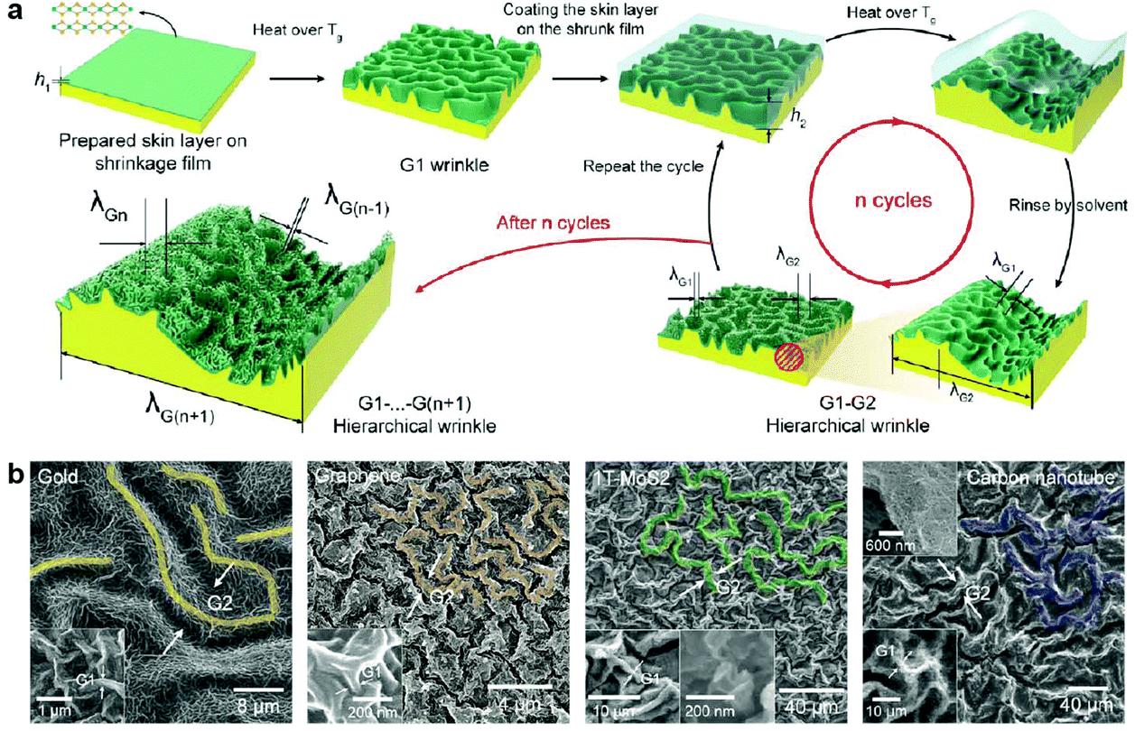 | ||
| Fig. 6 Sacrificial soft skin layers for hierarchical texturing of 2D nanomaterials. (a) Scheme illustrating the fabrication process. (b) Functional skin materials with hierarchical structures. Adapted with permission from ref. 75. Copyright 2018 American Chemical Society. | ||
6. Summary and outlook
In summary, this Mini-review described reconfigurable structures from wrinkling soft skin layers on deformable polymer substrates. With nanometer-scale control over the skin thickness based on plasma-mediated polymerization, soft skin systems can realize both nano- and microscale wrinkles with controlled wavelengths and orientations. Access to high strain regimes without cracking and delamination enables reversible switching of wrinkle orientation and design of hierarchical architectures. Because the soft skin layers exhibit conformal adhesion to a wide range of materials, 2D nanomaterials can also be patterned into unconventional hierarchical textures. Soft-skin-based wrinkling provides an opportunity to tailor properties of functional materials by external stimuli that can benefit electronic devices, photonics, and nano-bio interfaces.Conflicts of interest
There are no conflicts of interest to declare.Acknowledgements
This work was supported by the Office of Naval Research (ONR N00014-17-1-2482), the National Science Foundation (NSF CMMI-1462633, CMMI-1848613), and the Vannevar Bush Faculty Fellowship from the Department of Defense (DOD N00014-17-1-3023). D.R. appreciates scholarship from Jeongsong Cultural Foundation (Republic of Korea). S.D. thankfully acknowledges Cottrell Fellowship from Research Corporation for Science Advancement.References
- A. Sidorenko, T. Krupenkin, A. Taylor, P. Fratzl and J. Aizenberg, Science, 2007, 315, 487 CrossRef CAS.
- A. Grinthal and J. Aizenberg, Chem. Soc. Rev., 2013, 42, 7072–7085 RSC.
- P. Kim, L. Zarzar, M. Khan, M. Aizenberg and J. Aizenberg, Proc. SPIE, 2011, 7927, 792705 CrossRef.
- L. D. Zarzar, P. Kim and J. Aizenberg, Adv. Mater., 2011, 23, 1442–1446 CrossRef CAS.
- X. He, M. Aizenberg, O. Kuksenok, L. D. Zarzar, A. Shastri, A. C. Balazs and J. Aizenberg, Nature, 2012, 487, 214–218 CrossRef CAS.
- J. Kim, J. Yoon and R. C. Hayward, Nat. Mater., 2010, 9, 159–164 CrossRef CAS.
- P. Kim, L. D. Zarzar, X. Zhao, A. Sidorenko and J. Aizenberg, Soft Matter, 2010, 6, 750–755 RSC.
- Y.-J. Quan, Y.-G. Kim, M.-S. Kim, S.-H. Min and S.-H. Ahn, ACS Nano, 2020, 14, 5392–5399 CrossRef CAS.
- S. Baik, D. W. Kim, Y. Park, T.-J. Lee, S. H. Bhang and C. Pang, Nature, 2017, 546, 396–400 CrossRef CAS.
- B. Hu, C. Berkey, T. Feliciano, X. Chen, Z. Li, C. Chen, S. Amini, M. H. Nai, Q.-L. Lei, R. Ni, J. Wang, W. R. Leow, S. Pan, Y.-Q. Li, P. Cai, A. Miserez, S. Li, C. T. Lim, Y.-L. Wu, T. W. Odom, R. H. Dauskardt and X. Chen, Adv. Mater., 2020, 32, 1907030 CrossRef CAS.
- S. G. Lee, D. Y. Lee, H. S. Lim, D. H. Lee, S. Lee and K. Cho, Adv. Mater., 2010, 22, 5013–5017 CrossRef CAS.
- G. H. Lee, T. M. Choi, B. Kim, S. H. Han, J. M. Lee and S.-H. Kim, ACS Nano, 2017, 11, 11350–11357 CrossRef CAS.
- Q. Wang and X. Zhao, Sci. Rep., 2015, 5, 8887 CrossRef CAS.
- J. Genzer and J. Groenewold, Soft Matter, 2006, 2, 310–323 RSC.
- J. Rodríguez-Hernández, Prog. Polym. Sci., 2015, 42, 1–41 CrossRef.
- F. Brau, H. Vandeparre, A. Sabbah, C. Poulard, A. Boudaoud and P. Damman, Nat. Phys., 2011, 7, 56–60 Search PubMed.
- H. Jiang, D.-Y. Khang, J. Song, Y. Sun, Y. Huang and J. A. Rogers, Proc. Natl. Acad. Sci. U. S. A., 2007, 104, 15607 CrossRef CAS.
- P.-C. Lin and S. Yang, Appl. Phys. Lett., 2007, 90, 241903 CrossRef.
- P. Kim, Y. Hu, J. Alvarenga, M. Kolle, Z. Suo and J. Aizenberg, Adv. Opt. Mater., 2013, 1, 381–388 CrossRef.
- P.-C. Lin, S. Vajpayee, A. Jagota, C.-Y. Hui and S. Yang, Soft Matter, 2008, 4, 1830–1835 RSC.
- I. M. Graz, D. P. J. Cotton and S. P. Lacour, Appl. Phys. Lett., 2009, 94, 071902 CrossRef.
- Q. Zhang, Y. Tang, M. Hajfathalian, C. Chen, K. T. Turner, D. A. Dikin, G. Lin and J. Yin, ACS Appl. Mater. Interfaces, 2017, 9, 44938–44947 CrossRef CAS.
- M. J. Cordill, A. Taylor, J. Schalko and G. Dehm, Metall. Mater. Trans. A, 2010, 41, 870–875 CrossRef.
- A. Chiche, C. M. Stafford and J. T. Cabral, Soft Matter, 2008, 4, 2360–2364 RSC.
- N. J. Douville, Z. Li, S. Takayama and M. Thouless, Soft Matter, 2011, 7, 6493–6500 RSC.
- K. R. Phillips, N. Vogel, I. B. Burgess, C. C. Perry and J. Aizenberg, Langmuir, 2014, 30, 7615–7620 CrossRef CAS.
- Z. Wang, A. A. Volinsky and N. D. Gallant, J. Appl. Polym. Sci., 2014, 131, 41050 CrossRef.
- B. Jiang, L. Liu, Z. Gao and W. Wang, Adv. Opt. Mater., 2018, 6, 1800195 CrossRef.
- B. Jiang, L. Liu, Z. Gao, Z. Feng, Y. Zheng and W. Wang, ACS Appl. Mater. Interfaces, 2019, 11, 40406–40415 CrossRef CAS.
- D. J. Lipomi, B. C. K. Tee, M. Vosgueritchian and Z. Bao, Adv. Mater., 2011, 23, 1771–1775 CrossRef CAS.
- L. R. J. Scarratt, B. S. Hoatson, E. S. Wood, B. S. Hawkett and C. Neto, ACS Appl. Mater. Interfaces, 2016, 8, 6743–6750 CrossRef CAS.
- M. D. Huntington, C. J. Engel, A. J. Hryn and T. W. Odom, ACS Appl. Mater. Interfaces, 2013, 5, 6438–6442 CrossRef CAS.
- D. Rhee, W.-K. Lee and T. W. Odom, Angew. Chem., Int. Ed., 2017, 56, 6523–6527 CrossRef CAS.
- W.-K. Lee, C. J. Engel, M. D. Huntington, J. Hu and T. W. Odom, Nano Lett., 2015, 15, 5624–5629 CrossRef CAS.
- M. D. Huntington, C. J. Engel and T. W. Odom, Angew. Chem., Int. Ed., 2014, 53, 8117–8121 CrossRef CAS.
- T. Li, Z. Huang, Z. Suo, S. P. Lacour and S. Wagner, Appl. Phys. Lett., 2004, 85, 3435–3437 CrossRef CAS.
- L. V. Kayser and D. J. Lipomi, Adv. Mater., 2019, 31, 1806133 CrossRef.
- M. F. Ashby, Materials and the Environment, Elsevier, 2012 Search PubMed.
- H. Li, D. Buesen, R. Williams, J. Henig, S. Stapf, K. Mukherjee, E. Freier, W. Lubitz, M. Winkler, T. Happe and N. Plumeré, Chem. Sci., 2018, 9, 7596–7605 RSC.
- C. Poulard and P. Damman, EPL, 2007, 80, 64001 CrossRef.
- X. Gu, L. Shaw, K. Gu, M. F. Toney and Z. Bao, Nat. Commun., 2018, 9, 534 CrossRef.
- Z. Lu, C. Wang, W. Deng, M. T. Achille, J. Jie and X. Zhang, J. Mater. Chem. C, 2020, 8, 9133–9146 RSC.
- M. Richard, A. Al-Ajaji, S. Ren, A. Foti, J. Tran, M. Frigoli, B. Gusarov, Y. Bonnassieux, E. G. Caurel, P. Bulkin, R. Ossikovski and A. Yassar, Adv. Colloid Interface Sci., 2020, 275, 102080 CrossRef CAS.
- S. L. Oscurato, F. Formisano, C. de Lisio, M. d'Ischia, F. Gesuele, P. Maddalena, P. Manini, L. Migliaccio and A. Pezzella, Soft Matter, 2019, 15, 9261–9270 RSC.
- F. Li, H. Hou, J. Yin and X. Jiang, Sci. Adv., 2018, 4, eaar5762 CrossRef.
- P. D. Fowler, C. Ruscher, J. D. McGraw, J. A. Forrest and K. Dalnoki-Veress, Eur. Phys. J. E, 2016, 39, 90 CrossRef.
- D. J. Lipomi, J. A. Lee, M. Vosgueritchian, B. C. K. Tee, J. A. Bolander and Z. Bao, Chem. Mater., 2012, 24, 373–382 CrossRef CAS.
- M. E. Alf, A. Asatekin, M. C. Barr, S. H. Baxamusa, H. Chelawat, G. Ozaydin-Ince, C. D. Petruczok, R. Sreenivasan, W. E. Tenhaeff, N. J. Trujillo, S. Vaddiraju, J. Xu and K. K. Gleason, Adv. Mater., 2010, 22, 1993–2027 CrossRef CAS.
- A. M. Coclite, R. M. Howden, D. C. Borrelli, C. D. Petruczok, R. Yang, J. L. Yagüe, A. Ugur, N. Chen, S. Lee, W. J. Jo, A. Liu, X. Wang and K. K. Gleason, Adv. Mater., 2013, 25, 5392–5423 CrossRef CAS.
- J. Yin, J. L. Yagüe, D. Eggenspieler, K. K. Gleason and M. C. Boyce, Adv. Mater., 2012, 24, 5441–5446 CrossRef CAS.
- T. Easwarakhanthan, D. Beyssen, L. Le Brizoual and J. Bougdira, J. Vac. Sci. Technol., A, 2006, 24, 1036–1043 CrossRef CAS.
- S. Béfahy, P. Lipnik, T. Pardoen, C. Nascimento, B. Patris, P. Bertrand and S. Yunus, Langmuir, 2010, 26, 3372–3375 CrossRef.
- T. Ohishi, H. Noda, T. S. Matsui, H. Jile and S. Deguchi, J. Micromech. Microeng., 2016, 27, 015015 CrossRef.
- P. J. Rae and E. N. Brown, Polymer, 2005, 46, 8128–8140 CrossRef CAS.
- D. Rhee, J. T. Paci, S. Deng, W.-K. Lee, G. C. Schatz and T. W. Odom, ACS Nano, 2020, 14, 166–174 CrossRef CAS.
- P. Ge, S. Wang, J. Zhang and B. Yang, Mater. Horiz., 2020, 7, 2566–2595 RSC.
- K. Khare, J. Zhou and S. Yang, Langmuir, 2009, 25, 12794–12799 CrossRef CAS.
- X. Dai, N. Sun, S. O. Nielsen, B. B. Stogin, J. Wang, S. Yang and T.-S. Wong, Sci. Adv., 2018, 4, eaaq0919 CrossRef.
- Y. Wang, R. Yang, Z. Shi, L. Zhang, D. Shi, E. Wang and G. Zhang, ACS Nano, 2011, 5, 3645–3650 CrossRef CAS.
- P. Kang, M. C. Wang, P. M. Knapp and S. Nam, Adv. Mater., 2016, 28, 4639–4645 CrossRef CAS.
- Z. Wen, X. Wang, S. Mao, Z. Bo, H. Kim, S. Cui, G. Lu, X. Feng and J. Chen, Adv. Mater., 2012, 24, 5610–5616 CrossRef CAS.
- J.-K. Lee, S. Yamazaki, H. Yun, J. Park, G. P. Kennedy, G.-T. Kim, O. Pietzsch, R. Wiesendanger, S. Lee, S. Hong, U. Dettlaff-Weglikowska and S. Roth, Nano Lett., 2013, 13, 3494–3500 CrossRef CAS.
- L. Bai, Y. Xu, Y. Jiang, H. Chen, X. Li, J. Zhang and G. Song, Sens. Actuators, A, 2017, 260, 153–160 CrossRef CAS.
- S. Deng and V. Berry, Mater. Today, 2016, 19, 197–212 CrossRef CAS.
- P. Kang, K.-H. Kim, H.-G. Park and S. Nam, Light: Sci. Appl., 2018, 7, 17 CrossRef.
- W.-K. Lee, J. Kang, K.-S. Chen, C. J. Engel, W.-B. Jung, D. Rhee, M. C. Hersam and T. W. Odom, Nano Lett., 2016, 16, 7121–7127 CrossRef CAS.
- A. V. Thomas, B. C. Andow, S. Suresh, O. Eksik, J. Yin, A. H. Dyson and N. Koratkar, Adv. Mater., 2015, 27, 3256–3265 CrossRef CAS.
- N. Liu, A. Chortos, T. Lei, L. Jin, T. R. Kim, W.-G. Bae, C. Zhu, S. Wang, R. Pfattner, X. Chen, R. Sinclair and Z. Bao, Sci. Adv., 2017, 3, e1700159 CrossRef.
- W. H. Lee, J. W. Suk, J. Lee, Y. Hao, J. Park, J. W. Yang, H.-W. Ha, S. Murali, H. Chou, D. Akinwande, K. S. Kim and R. S. Ruoff, ACS Nano, 2012, 6, 1284–1290 CrossRef CAS.
- A. Krishna, J. M. Kim, J. Leem, M. C. Wang, S. Nam and J. Lee, Nano Lett., 2019, 19, 5086–5092 CrossRef CAS.
- S. V. Muley and N. M. Ravindra, JOM, 2014, 66, 616–636 CrossRef.
- S. Deng, D. Rhee, W.-K. Lee, S. Che, B. Keisham, V. Berry and T. W. Odom, Nano Lett., 2019, 19, 5640–5646 CrossRef CAS.
- Y. Xue, W.-K. Lee, J. Yuan, T. W. Odom and Y. Huang, Langmuir, 2018, 34, 15749–15753 CrossRef CAS.
- J. Kang, V. K. Sangwan, J. D. Wood and M. C. Hersam, Acc. Chem. Res., 2017, 50, 943–951 CrossRef CAS.
- W.-B. Jung, K. M. Cho, W.-K. Lee, T. W. Odom and H.-T. Jung, ACS Appl. Mater. Interfaces, 2018, 10, 1347–1355 CrossRef CAS.
| This journal is © The Royal Society of Chemistry 2020 |