
Recent progress in indoor organic photovoltaics
Hwa Sook
Ryu†
a,
Song Yi
Park†
b,
Tack Ho
Lee
b,
Jin Young
Kim
 *b and
Han Young
Woo
*a
*b and
Han Young
Woo
*a
aDepartment of Chemistry, Korea University, Seoul 02841, Republic of Korea. E-mail: hywoo@korea.ac.kr
bDepartment of Energy Engineering, Ulsan National Institute of Science and Technology (UNIST), Ulsan 44919, Republic of Korea. E-mail: jykim@unist.ac.kr
First published on 20th February 2020
Abstract
Among various potential applications of organic photovoltaics (OPVs), indoor power generation has great potential because of several advantages over outdoor light harvesting under 1 sun conditions. Commonly used indoor light sources have narrower emission spectra with lower intensity (by 3 orders of magnitude) as compared to the solar spectrum. Highly tunable optical absorption, large absorption coefficients, and small leakage currents under dim lighting conditions make OPVs promising candidates for indoor applications. For optimizing indoor photovoltaic materials and devices, several key issues (different from those under 1 sun conditions), such as developing new indoor photovoltaic materials and devices with suitable absorption spectra, large open-circuit voltages with low energy loss, minimized trap-mediated charge recombination and leakage currents, and device stability under indoor conditions, should be considered carefully. In this review, the recent progress in optimization of indoor photovoltaic materials and devices, and the key strategies to optimize the indoor photovoltaic characteristics will be summarized and discussed.
1. Introduction
In the last few decades, significant advancements have been achieved in organic photovoltaics (OPVs), which exhibit power conversion efficiencies (PCEs) of up to ∼17% for single junction cells via optimization of photovoltaic donor/acceptor (D/A) materials (especially developing non-fullerene (NF) acceptors), device architectures, and D/A blend morphologies.1–5 Semi-transparent and colorful building integrated photovoltaics, flexible/portable power sources, and indoor power generation for low-power consumption electronic devices may suggest an affordable solution for real industrial markets of OPVs.6Nowadays, buildings with lights on for 24 h (hospitals, stores, airports, offices, and factories) are common, and artificial lightings are prevalent energy sources to be harvested. Ambient indoor lighting sources, such as white light-emitting diodes (LEDs), fluorescent (FL) lamps, and halogen lamps, can provide sufficient energy for operating most small scale and low-power consumption indoor electronic devices.7,8 Currently, batteries are the power source of choice for operating such indoor electronic devices; however, battery-based power systems require periodic replacement and maintenance. Thus, there is a strong demand for semi-permanent indoor energy-harvesting systems that convert ambient energy to electricity, which enables low-power indoor devices to be self-sustaining.
Generally, OPVs exhibit inferior photovoltaic performance under solar illumination as compared to their inorganic counterparts. However, several previous studies demonstrated that OPVs can convert indoor lights into electricity more efficiently than other inorganic technologies because of their highly tunable optical absorption, large absorption coefficient, and small leakage currents under dim lighting conditions.9–11 Moreover, their light weight and mechanical flexibility make them highly desirable as ideal power sources for indoor Internet of Things (IoT) wireless sensor networks. Therefore, OPVs have great potential for ambient energy harvesting, which cannot be realized using robust silicon-based inorganic photovoltaics.
The emission spectra of indoor lighting sources are much narrower (often limited to the visible wavelength region) than the standard solar spectrum (Fig. 1(a)–(f)). Furthermore, their irradiance intensities are significantly lower by approximately 1000 times (typically 0.1–1 mW cm−2) as compared to that of the outdoor 1 sun conditions (AM 1.5G, 100 mW cm−2), which inevitably generate a significantly reduced photocurrent. Thus, obtaining the largest possible photocurrent is important in indoor photovoltaics.12–14 In addition, the light emission spectra and power densities are different for each indoor light source. For optimization of indoor power generation, a different strategy should be considered for the design of indoor light harvesting materials and device architectures from those of the current solar cells. Several previous reports investigated different photovoltaic behaviors of OPVs under 1 sun and various indoor lighting conditions, and discussed the ideal molecular and device structures to optimize the indoor light harvesting.12–14
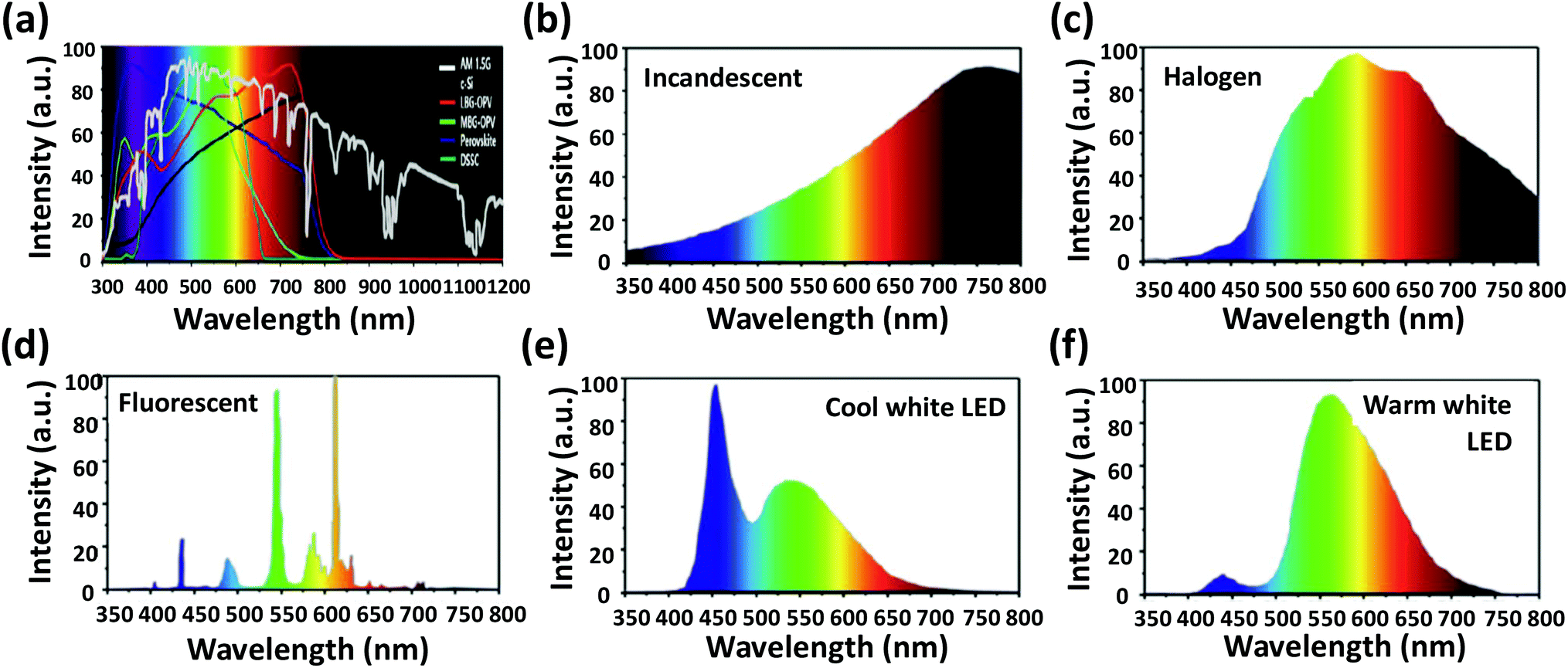 | ||
| Fig. 1 (a) AM 1.5G spectrum with the spectral response of various photovoltaic devices. Emission spectra of different indoor light sources: (b) incandescent lamp, (c) halogen lamp, (d) FL lamp, (e) cool white LED, and (f) warm white LED. Reproduced from ref. 12 with permission from Bentham Science. | ||
In this contribution, we review the recent progress in the developments of indoor organic semiconductors and device architectures, comparison of photovoltaic performances under outdoor and indoor conditions, underlying mechanisms of power conversion and key strategies to optimize the photovoltaic characteristics under indoor lighting conditions. Finally, we will discuss the remaining challenges and future research directions for practical applications of indoor OPVs.
2. Indoor photovoltaic materials
To maximize photocurrent generation, the band gap (Eg) of photoactive materials should be matched with light sources. According to the theoretical calculations, the ideal band gap of photoactive materials is 1.3–1.4 eV for solar irradiation and 1.9–2.0 eV for indoor lights. The increased band gap of indoor photovoltaic materials also results in a high open-circuit voltage (VOC), which is important for improving the efficiency under indoor light harvesting. Freunek et al. provided systematic investigations on the maximum theoretical performance of photovoltaic devices under indoor conditions.15,16 Theoretical maximum PCEs under various light sources were calculated by considering the Shockley–Queisser limit.17Fig. 2(a) shows the achievable maximum efficiencies under various light sources. The PCE limit that can be obtained from AM 1.5G is ∼35% at Eg = 1.4 eV. For the incandescent bulb and halogen lamp, the maximum PCEs decreased to ∼32%, respectively. Moreover, for the fluorescent tube, a phosphorus white LED, and an RGB white LED with narrower spectra, the efficiency limits were calculated to be 50, 57, and 64% respectively, at Eg = 1.9–2.2 eV. The sodium discharge lamp with monochromatic emission can yield PCEs up to 72% at Eg = 2.1 eV. This study highlights the great potential of photovoltaic devices for use in indoor power supply systems.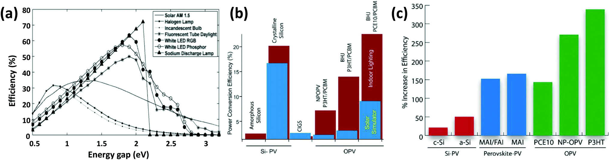 | ||
| Fig. 2 (a) Energy gap and limiting Shockley–Queisser efficiency of an ideal PV converter with different light sources. Reproduced from ref. 15 and 16 with permission from IEEE Xplore. (b) Comparison of PCE values of silicon and OPV devices under AM 1.5G (blue) and LED (red) light sources. (c) Percent increase in PCE under indoor LED light vs. AM 1.5G simulated solar spectrum. Reproduced from ref. 20 with permission from The Royal Society of Chemistry. | ||
Organic materials have high absorption coefficients and adjustable absorption ranges, which allow more effective light absorption and power conversion in indoor lighting environments. According to the best research-cell efficiencies chart from the NREL (National Renewable Energy Laboratory), crystal silicon solar cells (c-Si-SCs) exhibit higher PCEs (27.6%) than their organic counterparts under 1 sun illumination (17.4%);18 however, the situation changes under indoor conditions. In 2015, Mori et al. investigated the photovoltaic characteristics of polymer-based OPVs (PTB7-Th as a donor and PC71BM as an acceptor) under indoor LED lightings and compared the results with those of c-Si-SCs.19 Under 1 sun irradiation, the PCEs of the c-Si-SC and OPV were determined to be 13.49% and 8.43%, respectively. In contrast, the OPV exhibited a higher PCE (11.63%) than the c-Si-SC (9.65%) under LED illumination at 890 lx, because of a higher VOC (0.62 and 0.43 V for OPV and c-Si-SC, respectively). The PCE of the c-Si-SC decreased further to 6.92% at 186 lx. The higher VOC and well-matched absorption spectrum are the main advantages of OPVs over c-Si-SCs under indoor power generation. This demonstrates the possibility of applying OPVs to indoor light harvesting.
In 2016, Cutting et al. also reported that organic photovoltaic cells can outperform inorganic Si cells under LED illumination.20 They compared the photovoltaic performances under a white LED (20.5 mW cm−2) and solar irradiation of AM 1.5G. Under AM 1.5G illumination, the amorphous (a-Si) and crystal Si (c-Si) solar cells exhibited PCEs of 1.45 and 16.72%, respectively. Under LED illumination, both the a-Si and c-Si devices showed an improvement in PCEs by about 20%, thereby exhibiting PCEs of 2.18 and 20.19%, respectively. The OPVs were fabricated with P3HT:PC61BM and PCE10:PC71BM blends, and they showed much lower PCEs of 2.93 and 8.65%, respectively, compared to c-Si-SCs under AM 1.5G. However, the OPVs exhibited dramatic increases in their PCEs under LED illumination, and the resulting PCEs were 12.83 and 21.04%, respectively (Fig. 2(b)). The P3HT-based devices exhibited the largest PCE increase of 300% under LED light as compared to those with AM 1.5G, which is closely related to the spectral match between the light source and absorption of the photoactive material (Fig. 2(c)). In addition, the device performance of the c-Si-SC was strongly dependent on the light intensity.
After successful demonstration of the potentials of indoor OPVs, extensive studies have been performed to improve the indoor photovoltaic properties of OPVs. In the case of indoor OPVs, the VOC decreases compared to 1 sun conditions because the VOC shows a logarithmic dependence on the light intensity. To match the absorption with indoor lightings (through band gap tuning) and increase the VOC (through frontier molecular orbital (FMO) energy level control), various fullerene-, NF-, and multi-component-based indoor OPVs have been investigated. Electron donor and acceptor structures, which have been studied for indoor energy harvesting, are shown in Fig. 3 and 4 and their indoor photovoltaic properties are summarized in Tables 1–3.
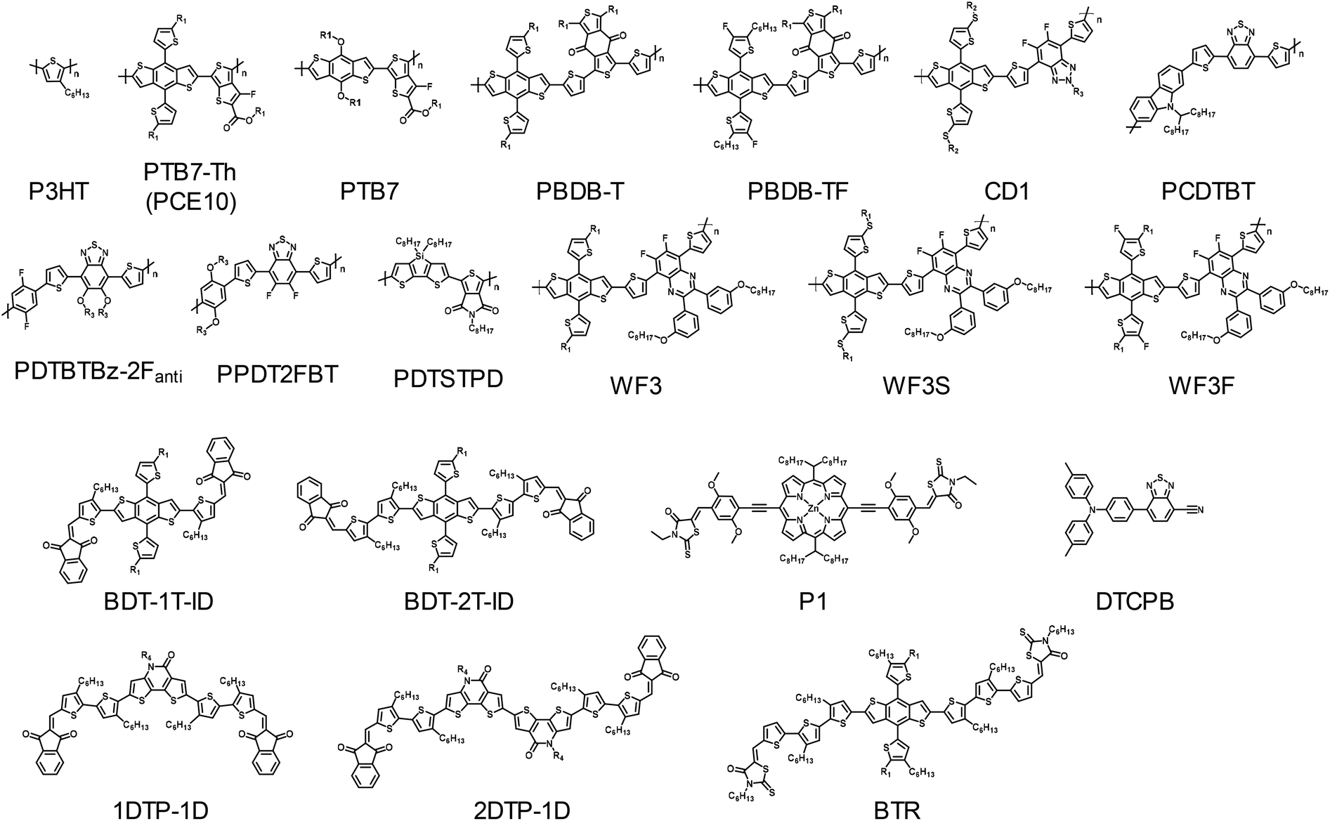 | ||
| Fig. 3 Donor structures for indoor organic photovoltaic devices (R1 = 2-ethylhexyl, R2 = 2-butyloctyl, R3 = 2-hexyldecyl, R4 = 2-octyldodecyl, R5 = 2-decyltetradecyl). | ||
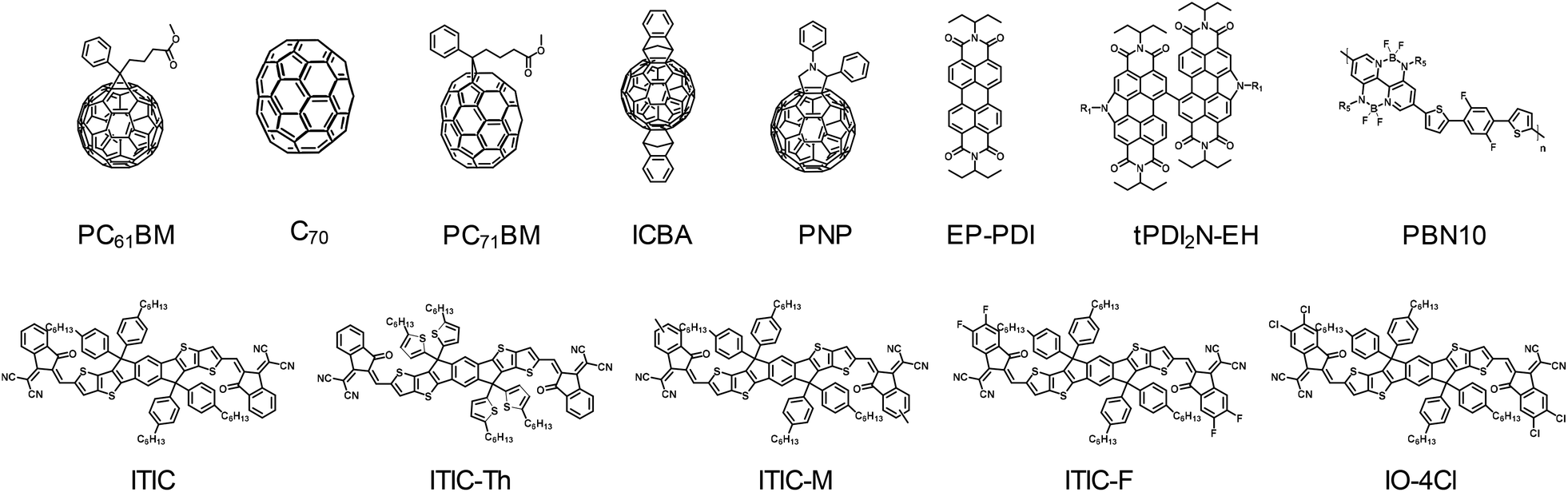 | ||
| Fig. 4 Acceptor structures for indoor organic photovoltaic devices. | ||
Donor![[thin space (1/6-em)]](https://www.rsc.org/images/entities/char_2009.gif) :acceptor :acceptor |
Light source | V OC [V] | J SC [μA cm−2] | FF [%] | PCE [%] | P out [μW cm−2] | Ref. |
|---|---|---|---|---|---|---|---|
| PTB7-Th/PC71BM | LED (186 lx) | 0.56 | 19.0 | 72.0 | 10.55 | 7.6 | 19 |
| PTB7-Th/PC71BM | LED (890 lx) | 0.62 | 92.0 | 74.0 | 11.63 | 42.3 | 19 |
| P3HT:PC71BM | FL (300 lx) | 0.41 | 20.6 | 56.6 | 5.80 | 4.8 | 21 |
| PCDTBT:PC71BM | FL (300 lx) | 0.72 | 27.7 | 69.3 | 16.60 | 13.9 | 21 |
| PTB7:PC71BM | FL (300 lx) | 0.61 | 28.6 | 69.5 | 14.60 | 12.2 | 21 |
| PDTBTBz-2Fanti:PC71BM | LED (1000 lx) | 0.82 | 112.4 | 70.4 | 23.10 | 66.0 | 22 |
| P3HT:PC71BM | LED (1000 lx) | 0.50 | 73.7 | 71.9 | 9.40 | 22 | |
| PBDB-T:PC71BM | LED (1000 lx) | 0.67 | 90.2 | 71.3 | 15.30 | 22 | |
| PTB7:PC71BM | LED (1000 lx) | 0.57 | 87.6 | 69.3 | 12.30 | 22 | |
| DTCPB:C70 | FL (200 lx) | 0.66 | 21.7 | 54.2 | 13.37 | 7.8 | 23 |
| DTCPB:C70 | FL (1000 lx) | 0.73 | 99.2 | 62.8 | 15.67 | 45.6 | 23 |
| WF3:PC71BM | LED (500 lx) | 0.57 | 58.3 | 64.2 | 12.83 | 24 | |
| WF3S:PC71BM | LED (500 lx) | 0.61 | 60.4 | 65.7 | 14.32 | 24 | |
| WF3F:PC71BM | LED (500 lx) | 0.69 | 63.6 | 67.4 | 17.34 | 24 | |
| P1:PC71BM (100 nm) | LED (300 lx) | 0.76 | 29.6 | 66.1 | 19.15 | 14.9 | 25 |
| P1:PC71BM (200 nm) | LED (300 lx) | 0.76 | 28.2 | 67.2 | 18.43 | 14.3 | 25 |
| P3HT:PC61BM | LED (500 lx) | 0.43 | 62.0 | 59.0 | 8.90 | 15.7 | 26 |
| P3HT:PC61BM | FL (500 lx) | 0.43 | 62.0 | 59.0 | 9.59 | 15.8 | 26 |
| P3HT:ICBA | LED (500 lx) | 0.73 | 50.0 | 63.0 | 13.05 | 23.0 | 26 |
| P3HT:ICBA | FL (500 lx) | 0.73 | 50.0 | 62.0 | 13.76 | 22.6 | 26 |
| PTB7:PNP | LED (200 lx) | 0.57 | 19.0 | 67.0 | 9.50 | 7.3 | 27 |
| BDT-2T-ID:PNP | LED (200 lx) | 0.75 | 24.2 | 68.0 | 16.00 | 12.3 | 27 |
| BDT-1T-ID:PNP | LED (200 lx) | 0.84 | 19.2 | 59.0 | 12.40 | 9.5 | 27 |
| 1DTP-1D:PNP | LED (200 lx) | 0.69 | 26.4 | 68.0 | 17.70 | 12.4 | 28 |
| 2DTP-1D:PNP | LED (200 lx) | 0.71 | 22.4 | 61.0 | 13.80 | 9.6 | 28 |
| BTR:PC71BM | FL (1000 lx) | 0.79 | 133.1 | 75.2 | 28.10 | 78.2 | 29 |
| Donor:acceptor |
Light source | V OC [V] | J SC [μA cm−2] | FF [%] | PCE [%] | P out [μW cm−2] | Ref. |
|---|---|---|---|---|---|---|---|
| PPDT2FBT:ITIC-M | LED (300 lx) | 0.53 | 20.8 | 57.0 | 6.9 | 6.3 | 30 |
| PPDT2FBT:ITIC-M | LED (1000 lx) | 0.62 | 68.5 | 54.6 | 7.5 | 23.2 | 30 |
| PPDT2FBT:ITIC-F | LED (300 lx) | 0.29 | 34.8 | 31.3 | 3.5 | 3.2 | 30 |
| PPDT2FBT:ITIC-F | LED (1000 lx) | 0.45 | 85.5 | 37.6 | 4.7 | 14.5 | 30 |
| PPDT2FBT:tPDI2N-EH | LED (300 lx) | 0.79 | 20.9 | 49.9 | 9.0 | 8.2 | 30 |
| PPDT2FBT:tPDI2N-EH | LED (1000 lx) | 0.84 | 65.4 | 50.2 | 8.9 | 27.6 | 30 |
| CD1:ITIC | FL (1000 lx) | 0.78 | 116 | 68.1 | 17.9 | 62.0 | 31 |
| CD1:ITIC | LED (1000 lx) | 0.77 | 107 | 67.5 | 15.4 | 56.0 | 31 |
| CD1:PBN-10 | FL (1000 lx) | 1.14 | 120 | 66.2 | 26.2 | 91.0 | 31 |
| CD1:PBN-10 | LED (1000 lx) | 1.14 | 105 | 65.4 | 21.7 | 78.0 | 31 |
| PBDB-TF:IO-4Cl (1cm2) | LED (200 lx) | 1.03 | 18.2 | 71.5 | 22.2 | 13.4 | 32 |
| PBDB-TF:IO-4Cl (1 cm2) | LED (1000 lx) | 1.10 | 90.6 | 79.1 | 26.1 | 78.8 | 32 |
| Donor:acceptor |
Light source | V OC [V] | J SC [μA cm−2] | FF [%] | PCE [%] | P out [μW cm−2] | Ref. |
|---|---|---|---|---|---|---|---|
| PCDTBT:PC71BM | FL (300 lx) | 0.70 | 30.7 | 56.4 | 16.5 | 12.2 | 34 |
| PCDTBT:PDTSTPD:PC71BM | FL (300 lx) | 0.72 | 32.8 | 61.7 | 19.8 | 14.6 | 34 |
| PCDTBT:PC71BM | LED (300 lx) | 0.70 | 31.2 | 56.6 | 16.0 | 12.4 | 34 |
| PCDTBT:PDTSTPD:PC71BM | LED (300 lx) | 0.72 | 31.4 | 62.1 | 18.1 | 14.1 | 34 |
| PTB7:PC71BM | LED (500 lx) | 0.60 | 46.0 | 54.3 | 8.9 | 35 | |
| PTB7:PC71BM:EP-PDI | LED (500 lx) | 0.65 | 57.0 | 68.5 | 15.4 | 35 | |
| PTB7-Th:PBDB-T:ITIC-Th:PC71BM | LED (1000 lx) | 0.68 | 102.3 | 57.5 | 14.3 | 36 | |
| PTB7-Th:PBDB-T:PC71BM:ITIC-Th | LED (500 lx) | 0.63 | 43.7 | 64.6 | 10.5 | 37 | |
| PTB7-Th:PBDB-T:PC71BM:ITIC-Th | LED (1000 lx) | 0.67 | 99.2 | 64.8 | 15.5 | 37 | |
| PTB7-Th:PBDB-T:PC71BM:ITIC-Th | FL (500 lx) | 0.64 | 49.5 | 65.5 | 10.9 | 37 |
2.1 Fullerene-based OPV devices
In 2016, Lee et al. compared the device performances of P3HT, PCDTBT, and PTB7 as the donor materials by blending with fullerene derivatives under dim lighting conditions.21 PCDTBT:PC71BM showed the best performance among them, generating a Pmax of 13.9 μW cm−2 with a PCE of 16.6% with a remarkably high VOC of 0.72 V under FL lamps (300 lx). The PTB7-based device exhibited the higher PCE than the PCDTBT-based device under AM 1.5G; however, the PCE under FL lamps was lower than that of the PCDTBT-based device because of its narrow band gap. Notably, the band gap of PCDTBT is 1.9 eV, which matches well with the emitting spectrum of FL lights. Finally, a 14 × 14 cm2 OPV module with a 100 cm2 active area successfully demonstrated a remarkable performance with a PCE of 11.2% and a Pmax of 938 μW under 300 lx FL lamps (short-circuit current density (JSC) of 314 μA, VOC of 4.87 V, and fill factor (FF) of 61.2%).Furthermore, in 2019, You et al. compared the indoor photovoltaic properties of four different donor polymers of PDTBTBz-2Fanti, P3HT, PBDB-T, and PTB7 (which have different band gap energy values) to emphasize the importance of the spectral match between PV materials and irradiance lightings.22 Among these polymers, the absorption spectrum of PDTBTBz-2Fanti with a wide band gap of 2 eV was well matched with the LED irradiance spectrum. This spectral match resulted in a very high PCE of 23.1% for PDTBTBz-2Fanti:PC71BM under a LED (1000 lx). Chen et al. reported a series of small molecular donors with finely tuned FMO energy levels and their band gaps.23 Among the four molecules, DTCPB showed the large bandgap of 2.04 eV and the highest PCE of 6.55% with C71 under AM 1.5G irradiation. Under FL lamps, the efficiency of the DTCPB based device improved significantly up to 13–16% depending on the irradiance intensity (200–1200 lx) via efficient light harvesting of visible wavelength lights. These results indicated that wide band gap materials (Eg = ∼2 eV) are advantageous for achieving high PCEs under indoor conditions.
The decreased VOC under indoor artificial lightings (compared to that under 1 sun) is a major limiting factor for device efficiency under indoor light conditions. Increasing the VOC of the OPV devices is a critical factor along with the spectral match to increase JSC for maximizing the device performance under indoor conditions. The value of VOC is directly related to the energy difference between the highest occupied molecular orbital (HOMO) of the donor and the lowest unoccupied molecular orbital (LUMO) of the acceptor. To obtain high VOC, the HOMO of the donor must be deep enough. Singh et al. designed electron donor polymers based on benzodithiophene with alkyl (WF3), alkylthio (WF3S), and fluoro (WF3F) substituted thiophenes by modulating their HOMO energy levels.24 The optical band gaps of the polymers are similar in the range of 1.73–1.78 eV; however, WF3F has the most down-shifted HOMO level of −5.62 eV among the three polymers because of electronegative fluorine substituents. Consequently, the WF3F:PC71BM device exhibited the highest PCE of 9.44% (with a VOC of 0.88 V) and 17.3% (with a VOC of 0.69 V) under 1 sun and LED (500 lx) illumination, respectively. Yin et al. designed an A–D–A type porphyrin-based donor material, P1, which shows broad and strong absorption from the visible to near-infrared region with a deep HOMO, thereby allowing a high VOC of 0.9 V under 1 sun conditions.25 The P1:PC71BM and PCDTBT:PC71BM cells exhibited higher PCEs of 19.2 and 18.7% (with VOC of 0.76 and 0.74 V) under LEDs as compared to those under 1 sun illumination. Furthermore, when the thickness of the film increased to 200 nm, the efficiency of the P1-based device remained at 18.4%; however, the efficiency decreased drastically to 13.2% for the PCDTBT-based devices. The origin of thickness independent characteristics could be attributed to the low electronic disorder of P1.
In addition, Yang et al. emphasized another strategy to increase the VOC by using an acceptor with a high LUMO level.26 Under 1 sun conditions, the P3HT:PC61BM device exhibited a VOC of 0.61 V, a JSC of 9.92 mA cm−2, and a FF of 0.64, thereby resulting in a PCE of 3.86%. The P3HT:ICBA device exhibited a PCE of 4.9% with a higher VOC (0.89 V) because of the high LUMO level (−3.74 eV) of ICBA as compared to PC61BM (−3.90 eV). Consequently, the P3HT:ICBA devices exhibited a PCE of 13.8% with significantly increased VOC (0.73 V) as compared to the P3HT:PC61BM devices (PCE: 9.59%, VOC: 0.43 V) under TL5 FL tube (500 lx) illumination. Although the P3HT:ICBA device exhibited a lower JSC of 50 μA cm−2, it provided a better power output (Pout) of 22.57 μW cm−2 because of its higher VOC as compared to the P3HT:PC61BM devices (Table 1).
Arai et al. reported two types of small-molecule donors (BDT-2T-ID and BDT-1T-ID) with an Eg of 1.7–1.8 eV and deep-lying HOMOs at −5.13 and −5.23 eV.27 BDT-2T-ID- and BDT-1T-ID-based devices exhibited lower PCEs of 6.1% and 3.9%, respectively, as compared to the PTB7-based devices (6.7% PCE) under 1 sun illumination. However, their VOCs are higher (1 V) than that of the PTB7-based device, which is attributed to their deeper HOMO levels. Under LED illumination, the BDT-2T-ID- and BDT-1T-ID-based devices showed a remarkable increase in PCEs up to 16.2% and 12.9% with VOCs of 0.75 and 0.84 eV, respectively, thereby generating high Pout values of 12.4 and 9.9 μW cm−2, respectively. These small molecule-based devices presented three times greater efficiency than PTB7-based devices as they possessed the deep-lying HOMO energy levels, resulting in a larger VOC under LED illumination. The same group further synthesized new small-molecule donors with the same strategy of obtaining a low lying HOMO level, incorporating an electron-withdrawing fused lactam group with 1,3-indandione.28 Band gaps of 1DTP-ID and 2DTP-ID small molecules were determined to be 1.65 and 1.70 eV, and the HOMO levels were −5.25 and −5.35 eV, respectively. Under LED (200 lx) illumination, the 1DTP-ID- and 2DTP-ID-based devices gave high Pout values of 12.4 and 9.6 μW cm−2 with high PCEs of 17.7% and 13.8% (VOCs of 0.69 and 0.71 V), respectively. Lee et al. reported a BTR:PC71BM device with a considerably high PCE of 28.1% with a maximum power density of 78.2 μW cm−2 under an FL lamp (1000 lx),29 and they also simulated the charging time of rechargeable batteries using OPVs under indoor lights. For a button-sized battery, less than one day (or a few days) was required to charge the battery fully. This simulation suggests a high potential of OPVs for indoor power-supply applications, even though the charging time seems quite long.
2.2 Non-fullerene-based OPV devices
Compared to fullerene-based OPVs, NF-based OPVs have many advantages to further improve the indoor light harvesting. Fullerene derivatives have poor absorption in the visible wavelengths, which causes loss in photocurrent generation. They also have limited tunability of the electronic structures, i.e., FMO energy levels, which makes it difficult to modulate the VOC. In contrast, NF acceptors can be tailored to have strong light absorption in the visible regions and adjustable FMO levels to maximize the VOC. NF acceptors have great potential; thus, many research groups have investigated their indoor photovoltaic properties. The comparison of photovoltaic performances of previously reported NF-based OPVs under indoor light illumination is summarized in Table 2.In 2019, Dayneko et al. designed an N-annulated perylenediimide (PDI) molecule (tPDI2N-EH) as an electron acceptor, and emphasized the importance of spectrally well-matched absorption of NF acceptors with indoor light sources to achieve high efficiency.30 PDI is often used as a building block of electron acceptors because of its strong light absorption in the visible region and excellent electron-accepting/transporting abilities. A PPDT2FBT:tPDI2N-EH blend film had appropriate absorption from 400 to 700 nm. PPDT2FBT:tPDI2N-EH devices exhibited a low PCE of 6.48% despite their high VOC over 1 V under 1 sun illumination; however, better device performance was achieved with a PCE of 9.0% under LED (300 lx) illumination. In addition, the PPDT2FBT:tPDI2N-EH-based devices had minor PCE drops with the decrease in the light intensity of the LED from 10000 to 300 lx, while maintaining a high VOC of 0.79 V at 300 lx. In the same year, Ding et al. designed a medium band gap polymer acceptor (PBN-10) containing a B ← N group to increase the VOC.31 The large band gaps of the polymer donor (CD1, 1.93 eV) and acceptor (PBN-10, 1.95 eV) were incorporated, which provided a well-matched absorption with the emission spectra of indoor light sources. The HOMO and LUMO levels were −5.28 and −2.91 eV for CD1 and −5.81 and −3.42 eV for PBN-10, respectively. The large energy offset between the acceptor's LUMO and donor's HOMO was expected to increase the value of VOC. The all polymer-based device exhibited a PCE of 7.9% under 1 sun illumination and a significantly enhanced PCE of 27.4% with an excellent VOC of 1.14 V under an FL lamp at 1000 lx. This is the first successful demonstration of high-performance all-polymer OPV cells under indoor light sources, and the VOC of 1.14 V is the highest value among those reported so far under indoor light sources.
Most organic solar cells have an energy loss (Eloss = Eg − qVOC, where q is elementary charge) around (or higher than) 0.6 V under AM 1.5G conditions. In addition, an additional energy loss of 0.2 V could be involved when the light intensity is significantly lowered. Considering such energy losses, it is expected that a VOC of 1.0 V can be obtained using ∼1.8 eV of Eg materials, and it is suitable for indoor light sources. However, the VOC is mostly below 0.8 V in most reported indoor OPV devices, which is a major limiting factor for device efficiency under indoor light conditions. Recently Cui et al. successfully demonstrated highly efficient OPVs under indoor light illumination with low energy loss (<0.6 eV), by a combination of a new small molecular acceptor IO-4Cl (Eg = 1.8 eV, LUMO = −3.83 eV) and PBDB-TF as a donor which show optimal absorption for indoor light sources covering the visible light in the range of 400 to 700 nm.32,33 The devices exhibited a PCE of 9.80% with an exceptionally high VOC of 1.24 V under AM 1.5G illumination. Under LED lights (200–1000 lx), a high VOC was maintained over 1 V, thereby resulting in high PCEs over 20%. At 1000 lx, a 1 cm2 cell showed a PCE of 26.1% with a VOC of 1.10 V, and an even large-area cell (4 cm2) exhibited excellent device performance with a PCE of 23.9% and a VOC of 1.07 V, showing remarkably low radiative and nonradiative voltage losses. They have also emphasized the high thickness tolerance of indoor OPV devices that makes them suitable for large area devices via roll-to-roll printing. In addition, the device maintains its initial PCE for 1000 h under continuous LED illumination, thereby demonstrating great stability under indoor light conditions.
2.3 Multi-component OPV devices
In D/A binary devices, the limited absorption mainly limits the JSC. To overcome this limitation, ternary devices have been introduced for optimizing indoor power generation. The third component should increase the JSC value with complementary light absorption, and additionally improve the FF by the modulation of the bulk heterojunction (BHJ) blend morphology. The photovoltaic characteristics of multi-component OPVs under indoor light illumination are summarized in Table 3. Yin et al. introduced a ternary compound to improve the performance of the PCDTBT:PC71BM device.34 The HOMO energy of PCDTBT is −5.50 eV, which results in a high VOC in the binary BHJ device with PC71BM. However, the PCE was as low as 5.3% under 1 sun conditions because of its low hole mobility of 10−5 cm2 V−1 s−1. They chose a donor polymer PDTSTPD as a ternary component, which has a similar molecular structure to PCDTBT and possesses a low-lying HOMO level (−5.60 eV) and high hole mobility. Under a 2700 K FL lamp (300 lx), the PCDTBT:PC71BM device achieved a PCE of 16.5% and a Pout of 12.2 μW cm−2, with a JSC of 30.7 μA cm−2, a FF of 56.4%, and a VOC of 0.70 V. The ternary PCDTBT:PDTSTPD:PC71BM device showed an improved PCE of 19.8% and a Pout of 14.6 μW cm−2, with a JSC of 32.8 μA cm−2, a FF of 61.7%, and a VOC of 0.72 V, respectively. The PCE improvement of the ternary device was mainly attributed to the increase in the JSC and FF from enhanced optical absorption and charge transport. Similarly, Singh et al. designed a perylene-based small molecule acceptor, N,N′-bis(1-ethylpropyl)perylene-3,4,9,10-tetracarboxylic diimide (EP-PDI), as a third component for a binary blend of PTB7 and PC71BM.35 Compared to the PTB7:PC71BM binary blend, the ternary blend with EP-PDI showed strong light absorption from 400 to 600 nm, which is spectrally well-matched with those of LED lamps. Addition of EP-PDI to the PTB7:PC71BM binary blend played a critical role in the modulation of the blend film morphology, thereby leading to more efficient charge transport in a vertical direction. Consequently, the optimal PTB7:PC71BM:EP-PDI-based device showed a significantly improved PCE of 15.68% with a VOC of 0.65 V, a JSC of 57 μA cm−2, and a FF of 68.5% under indoor LED light conditions (500 lx), as compared to the binary PTB7:PC71BM devices (PCE = 9.11%).To further optimize the light absorption for indoor light harvesting, quaternary BHJ (Q-BHJ) systems were also demonstrated by incorporating two donors and two acceptors. Nam et al. successfully demonstrated a Q-BHJ device with a wide absorption range and improved the charge generation and morphological stability.36 Under AM 1.5G illumination, PBDB-T:PC71BM exhibited a PCE of 7.38% and PTB7-Th:ITIC-Th exhibited a PCE of 7.50%. The PTB7-Th:PBDB-T:ITIC-Th:PC71BM quaternary device exhibited a significantly improved PCE of 9.46%, with a VOC of 0.81 V, a JSC of 19.4 mA cm−2, and a FF of 60.3%, respectively. The Q-BHJ device also showed improved device stability. For testing the thermal stability, the encapsulated devices were thermally heated at 60 °C under dark ambient conditions. The Q-BHJ device maintained 87.7% of its initial PCE after 1020 min, while the PCE of PTB7-Th:ITIC-Th decreased up to 54.5% of its initial value. Under 1000 lx LED illumination, an optimal PCE of 14.29% was obtained for the Q-BHJ devices, thereby showing great potential for achieving high efficiency with increased device lifetime. Furthermore, they successfully demonstrated semi-transparent Q-OPVs with a PCE of 15.46% under LED (1000 lx) while retaining high transparency.37
3. Device engineering for indoor OPVs
The generated photocurrent density (Jph) in OPVs is proportional to light intensity. In general, indoor lighting systems (such as LEDs, FL lamps, etc.) provide intensities in the range of 200–1000 lx, while bright daylight provides a light intensity of approximately 120000 lx. Therefore, the generated Jph under indoor lights is in the range of ∼μA cm−2, implying that high shunt resistance (Rsh) is a prerequisite to achieve efficient indoor photovoltaics with minimized leakage currents. In addition, the series resistance (Rs) effect is not significant under such indoor lighting systems with a negligible Rs-induced voltage drop.38 Steim et al. systematically investigated the Rs and Rsh effects on the device properties under various light intensities by numerical simulation and electrical modelling.39 The current density–voltage (J–V) characteristics were significantly affected by varying Rsh under low light intensities; low-Rsh devices exhibited poor J–V characteristics affected by significant leakage currents. On the other hand, Rs rarely affected the device performance under low light intensities, while J–V curves were greatly influenced by Rs under 1 sun conditions. In summary, both high Rsh and low Rs are essential conditions to obtain high PCEs under 1 sun, whereas high Rsh is the most important factor determining the device properties under low light intensity regardless of Rs. These were proved by experimental results, wherein the P3HT:PC61BM BHJ devices exhibited ∼7% PCE under a 1000 lx FL lamp with a high Rsh of 85 kΩ cm2 (∼2.7% PCE under AM 1.5G). From the simulation of the relationship between VOC and light intensity, high Rsh devices exhibited a low VOC drop with decreasing light intensity, and an Rsh of ∼100 kΩ cm2 of was required to obtain full VOC of P3HT:PC61BM devices under low light intensities. Furthermore, the Rs effect is not significant under low light intensity; thus, low-conductivity electrodes can be also used as electrodes. In this section, the highly efficient OPV devices under low light intensity will be discussed by increasing the Rsh.
3.1 Active layer thickness
The absorption coefficient of organic semiconductors is much higher than those of their inorganic counterparts; thus, a roughly ∼100 nm thick active layer is sufficient to entirely absorb the incident solar light.40 The thicker active layer of 300–1000 nm often hinders efficient power conversion in OPVs, due to lower carrier mobilities and shorter exciton diffusion lengths of organic semiconductors compared to those of their inorganic counterparts. Therefore, most high PCE results reported previously were achieved with 100–200 nm thick active layers.41–44 Small et al. reported that space-charge accumulation is one of the main reasons for lowered PCEs in PDTG-TPD:PC71BM OPVs with >200 nm thickness.45 The light intensity dependent Jph curves showed that the space-charge limited (SCL) Jph characteristics (in 409 nm thick devices) were suppressed when the intensity was reduced from 100 to 11.4 mW cm−2, with a 24% enhancement of the FF. This is attributed to the reduced space-charge build-up in the active layer with reduced charge carrier concentration with decreasing light intensities. This result implies that the thick active layer may increase the Rsh without significant build-up of space charges under low light intensity or indoor light illumination.The thick active layer is more suitable for indoor photovoltaic applications. Vincent et al. suggested optimal design of OPVs for efficient indoor light harvesting.46 P3HT:ICBA was selected because of its high spectral overlap with a LED light source. The optimum device structure, especially the optimum thickness of the active layer, was different depending on the light intensities; a PCE of 4.2% was obtained with a 130 nm thick active layer under AM 1.5G illumination and a PCE of 5.4% was obtained with a 230 nm thick active layer under 1000 lx LED light illumination. With the increase in the thickness of the active layer from 80 to 400 nm, the leakage currents decreased significantly by three orders of magnitude in a shunt regime from dark J–V curves. Shin and coworkers also reported efficient indoor OPV devices using an ultra-thick photoactive layer47 based on a PPDT2FBT:PC71BM BHJ blend which showed outstanding device performance with over 9% PCEs even with a 300 nm thick active layer under 1 sun illumination.48,49 The PPDT2FBT:PC71BM-based OPVs exhibited a 16% PCE with a 390 nm thick active layer under 1000 lx LED illumination. Even the devices with an 870 nm thick active layer exhibited excellent indoor device performance with a PCE of 12.5%, while only a 3.4% PCE was obtained under 1 sun illumination (Fig. 5). According to the Shockley equation, JSC is inversely proportional to 1 + Rs/Rsh.50 Under 1 sun illumination, Rs/Rsh increases substantially with the increase in the thickness of the active layer; thus, the JSC (13 mA cm−2 at 870 nm) decreased by 30% compared to the maximum JSC (18.6 mA cm−2 at 390 nm). In contrast, under 1000 lx LED illumination, Rs/Rsh was much lower (<0.007) compared to that under 1 sun, and the JSC values were thickness tolerant (110–120 μA cm−2) from 280 to 870 nm thickness.
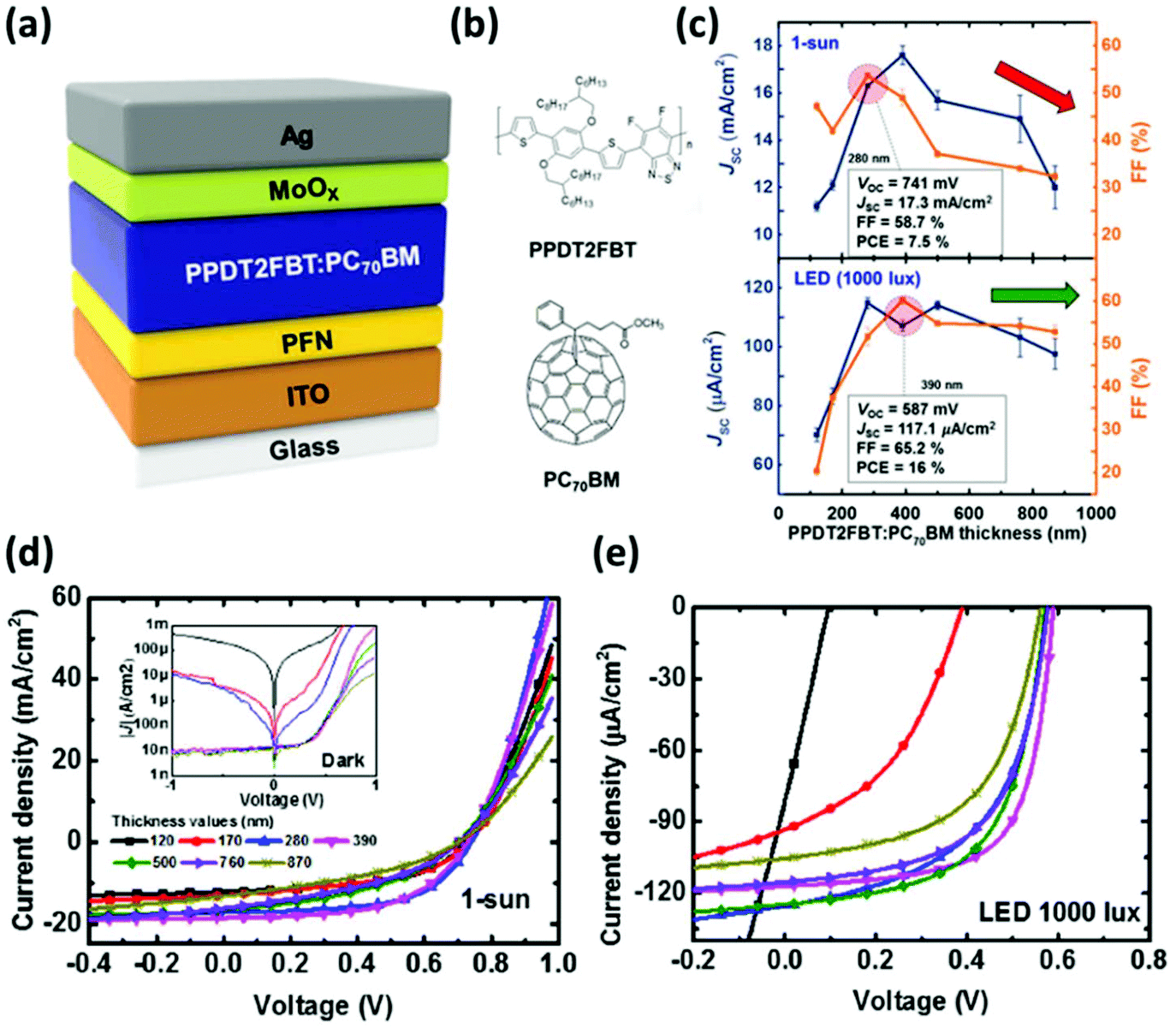 | ||
| Fig. 5 Active layer thickness effect under 1 sun and LED illumination. (a) The device architecture and (b) molecular structures of PPDT2FBT and PC71BM. (c) Active layer thickness dependent JSC and FF under 1 sun and LED illumination. J–V characteristics with various photoactive layer thicknesses under (d) AM 1.5G and (e) LED (1000 lx) illumination. (Inset of (d): dark J–V curves.) Reproduced from ref. 47 with permission from Elsevier. | ||
3.2 Interfacial engineering
Along with the thickness of the active layer, the charge transport layer also affects device performance significantly, since it is directly related to the Rs and Rsh in the devices. In 2016, Lechêne et al. reported device optimization (PCDTBT:PC71BM BHJ) for indoor photovoltaic applications by varying the thickness of an electron transporting ethoxylated polyethylenimine (PEIE) layer in a conventional device configuration.51 The PEIE thickness rarely affected the device performance under 1 sun illumination, while the performance was affected significantly under indoor light conditions. Thick PEIE devices exhibited a high Rsh of 500 kΩ cm2 (calculated from a dark J–V curve), and a PCE of 7.6% under simulated indoor light (310 μW cm−2) while thin PEIE devices did not operate well (PCE of 0.7%) due to significant leakage currents. Goo and coworkers also reported device optimization by varying the PEIE thickness in an inverted device configuration.52 They used P3HT:ICBA as an active layer which is spectrally matched with common indoor lights. Under 1 sun, the devices with a 5.6 nm thick PEIE layer showed the highest PCE of 4.7%. Under 500 lx LED light, the optimum devices needed a thicker (8.5 nm) PEIE layer, resulting in the highest PCE of 13.4%. The PEIE layer thickness greatly influenced the dark J–V curves and Rsh; a thicker PEIE layer provided lower leakage currents with high Rsh (Fig. 6).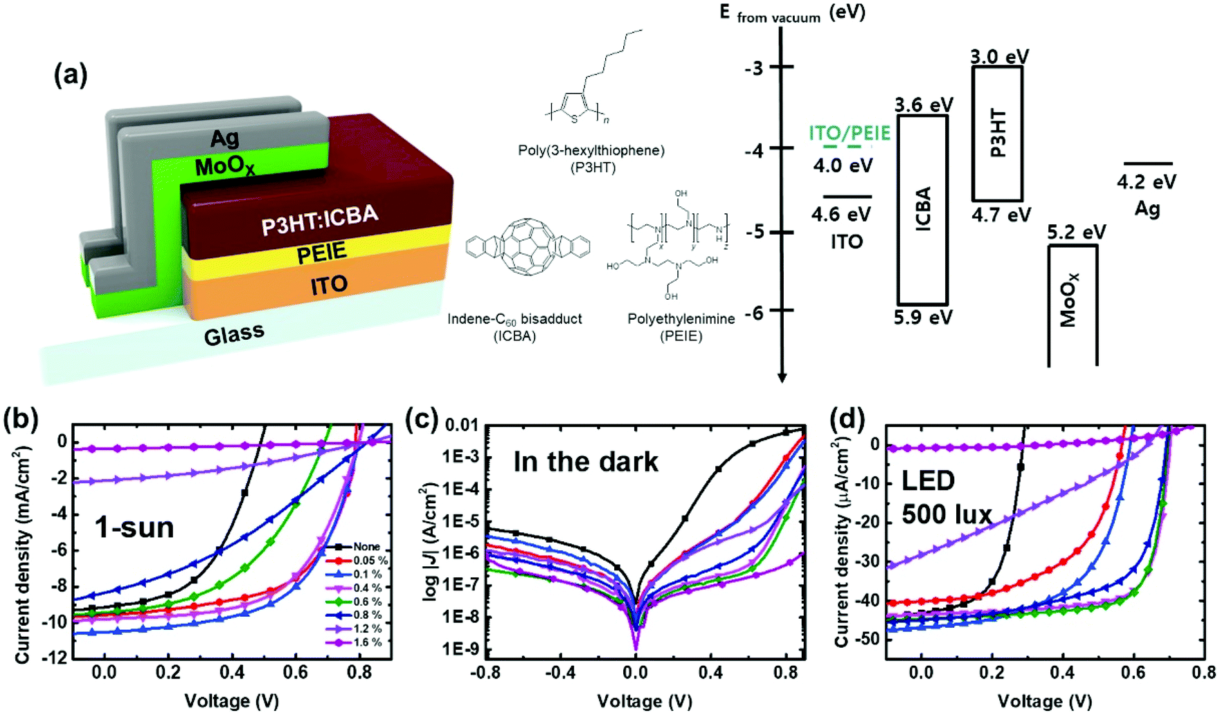 | ||
| Fig. 6 PEIE thickness effect under LED illumination. (a) Device architecture, molecular structures of P3HT, ICBA and PEIE, and corresponding energy band diagram. J–V characteristics measured under (b) AM 1.5G illumination, (c) darkness and (d) LED (500 lx) illumination. Reproduced from ref. 52 with permission from Elsevier. | ||
Furthermore, a bilayer of ZnO nanoparticles (ZnO NPs) and PEIE (ZnO NPs/PEIE) was investigated as an electron transport layer (ETL) for indoor OPVs, by comparing a single ETL of ZnO NPs or PEIE. Shin et al. compared the properties of the inverted P3HT:ICBA-based devices with three electron transport layers of ZnO NPs, PEIE, and ZnO NPs/PEIE under 1 sun and 1000 lx LED illumination.53 The single layer of ZnO NPs was not suitable (PCE: 5.6%) for indoor photovoltaic applications because of the Schottky barrier induced by an energy level mismatch between ZnO NPs and ICBA. An unsuitable work function (WF) of ZnO NPs originated from the absence of ultraviolet light in the LED lamp. However, the WF of electrodes was successfully reduced due to the formation of a dipole moment by deposition of the PEIE layer. In addition, the ZnO NPs/PEIE layer effectively reduced leakage currents compared to the single layer of ZnO NPs or PEIE. As a result, the device with ZnO NPs/PEIE exhibited excellent device performance with a PCE of 14.1% under 1000 lx LED illumination.
3.3 Various device architectures
In contrast to outdoor OPVs under 1 sun, low-conductivity electrodes can be used as electrodes in indoor OPV systems; sheet resistances of electrodes show little influence on the device performance under low light intensity when the Rsh of devices is large enough. The ZnO layer (which is generally used as an ETL) without transparent electrodes (such as ITO) can work well as a cathode of indoor OPVs (Fig. 7).54 Surprisingly, the P3HT:ICBA BHJ devices with a ZnO (200 nm)-electrode exhibited a 9.5% PCE under an LED lamp (500 lx), while the devices did not work under 1 sun illumination (PCE: 0.4%). The thickness of the ZnO layer also significantly affected the device performances; a thickness of at least 200 nm was necessary to avoid leakage currents under indoor LED illumination. The 50 and 100 nm thick ZnO-electrode devices showed poor device performances with PCEs of 1.9 and 2.6%, respectively, because of significant leakage currents.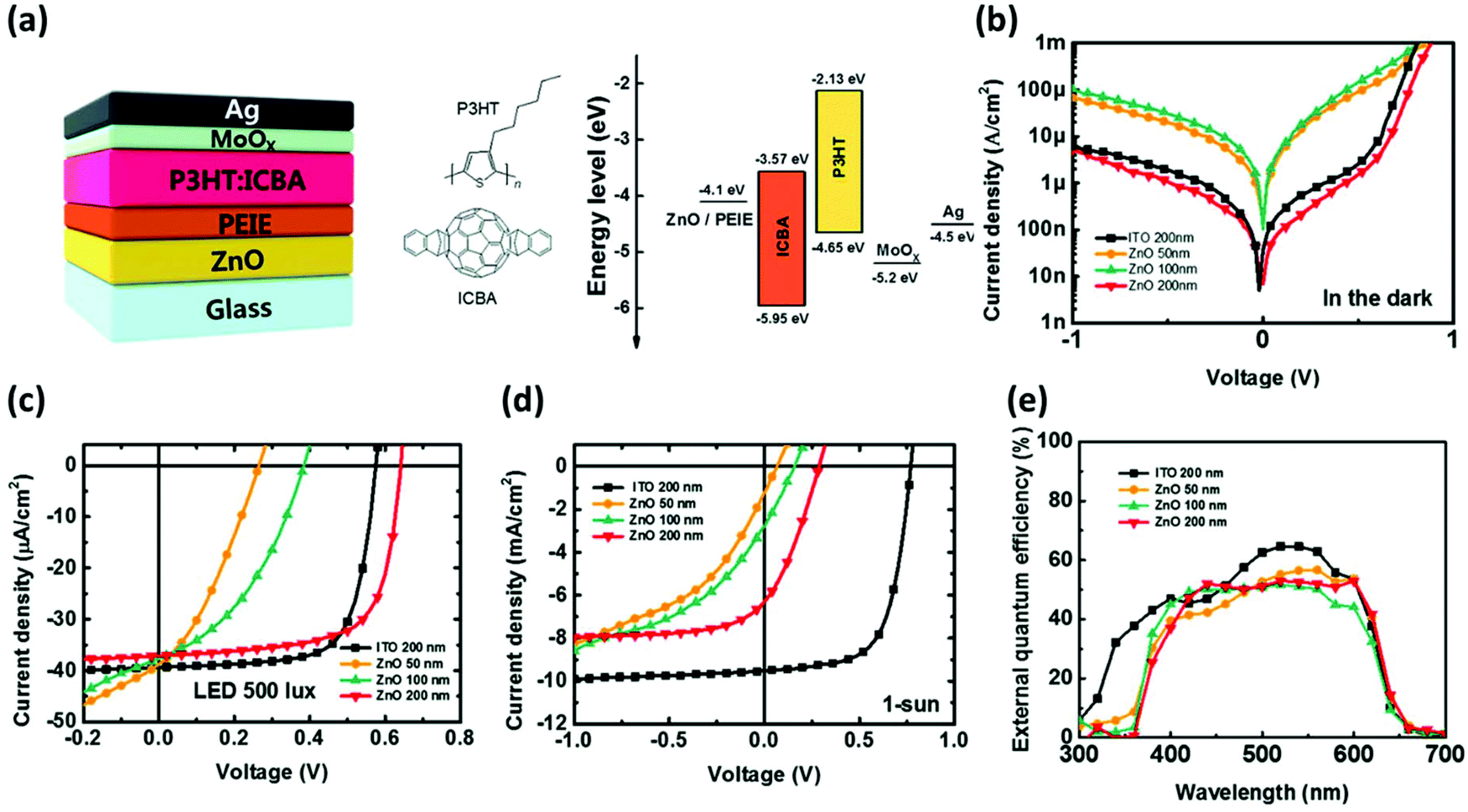 | ||
| Fig. 7 Anode-free OPV devices. (a) Device structure of anode-free OPVs and the corresponding energy band diagram. J–V characteristics with ITO and ZnO electrodes (with different thicknesses of 50, 100 and 200 nm) under (b) darkness, (c) 500 lx LED and (d) AM 1.5G illumination. (e) Corresponding EQE spectra. Reproduced from ref. 54 with permission from The Royal Society of Chemistry. | ||
Oxide/metal/oxide (OMO) electrodes are widely used as transparent conducting electrodes (TCEs).55–57 Using the ZnO/Ag/ZnO (ZAZ) electrode as the cathode in inverted OPVs, efficient indoor photovoltaic devices were successfully demonstrated.58 Under 1 sun illumination, the device performances were similar (∼4% PCEs) for both devices with ITO and ZAZ electrodes for P3HT:ICBA-based OPVs. On the other hand, under 500 lx LED lamps, the ZAZ devices showed the best PCE of 12.1% which was higher than those of ITO devices (10.4% PCE). A significant micro-cavity effect enabled JSC improvement with enhanced light absorption.
Incorporating metal nanoparticles (such as Ag, Au, Cu, etc.) in OPV devices can enhance the photocurrent effectively by a surface plasmon resonance (SPR) effect.59–61 It was successfully proved that this strategy also works well under indoor lights.62 By incorporating Au nanoparticles decorated with graphene oxides with poly(ethylene glycol) side chains (Au@PEG-GO) in both PEDOT:PSS and photoactive layers (PBDTTT-EFT:PC71BM), the PCEs greatly improved from 13.4 to 16.2% with enhanced JSC values from 119 to 143 μA cm−2 under FL (1000 lx), compared to that of the device without Au@PEG-GO. A similar enhancement was also observed under a white LED (1000 lx) with a PCE enhancement from 12.3 to 15.6% with enhanced JSC from 117 to 156 μA cm−2.
3.4 Large-area devices and stability
For further development of indoor OPVs, the device area should be scaled up. Efficient large-area indoor OPVs based on the PBDB-TF:IO-4Cl BHJ were successfully demonstrated with high PCEs of 26.1 and 23.9% (under a 2800 K LED lamp, 1000 lx) with a device area of 1 cm2 (spin-coated) and 4 cm2 (blade-coated), respectively, as discussed in section 2.2.32 The devices also showed excellent stability under continuous indoor light illumination, maintaining their original PCEs after 1000 h (Fig. 8(a) and (b)). The device stability is expected to be better under indoor light, compared to that under 1 sun illumination. In addition, Cui et al. reported efficient large-area (1 cm2) OPVs with excellent stability under continuous illumination of indoor light.63 Using PBDB-TF:ITCC BHJs, over 20% PCEs were obtained under 200, 500 and 1000 lx LED (2700 K) illumination, while the same devices showed a 10.3% PCE under AM 1.5G illumination. Notably, the devices showed good stability under 500 lx (2700 K) LED illumination, while maintaining over 90% of their initial PCEs after 500 h (Fig. 8(c)). (Testing conditions: the devices were encapsulated and measured in air at an ambient temperature of 25–30 °C with a relative humidity of 40–60%.) However, the devices were photodegraded under strong illumination of the white LED, wherein the intensity is similar to that under AM 1.5G conditions. This strong illumination can increase the temperature of the device to ∼45 °C, leading to significant device degradation by approximately an order of magnitude of their original PCEs after 160 h.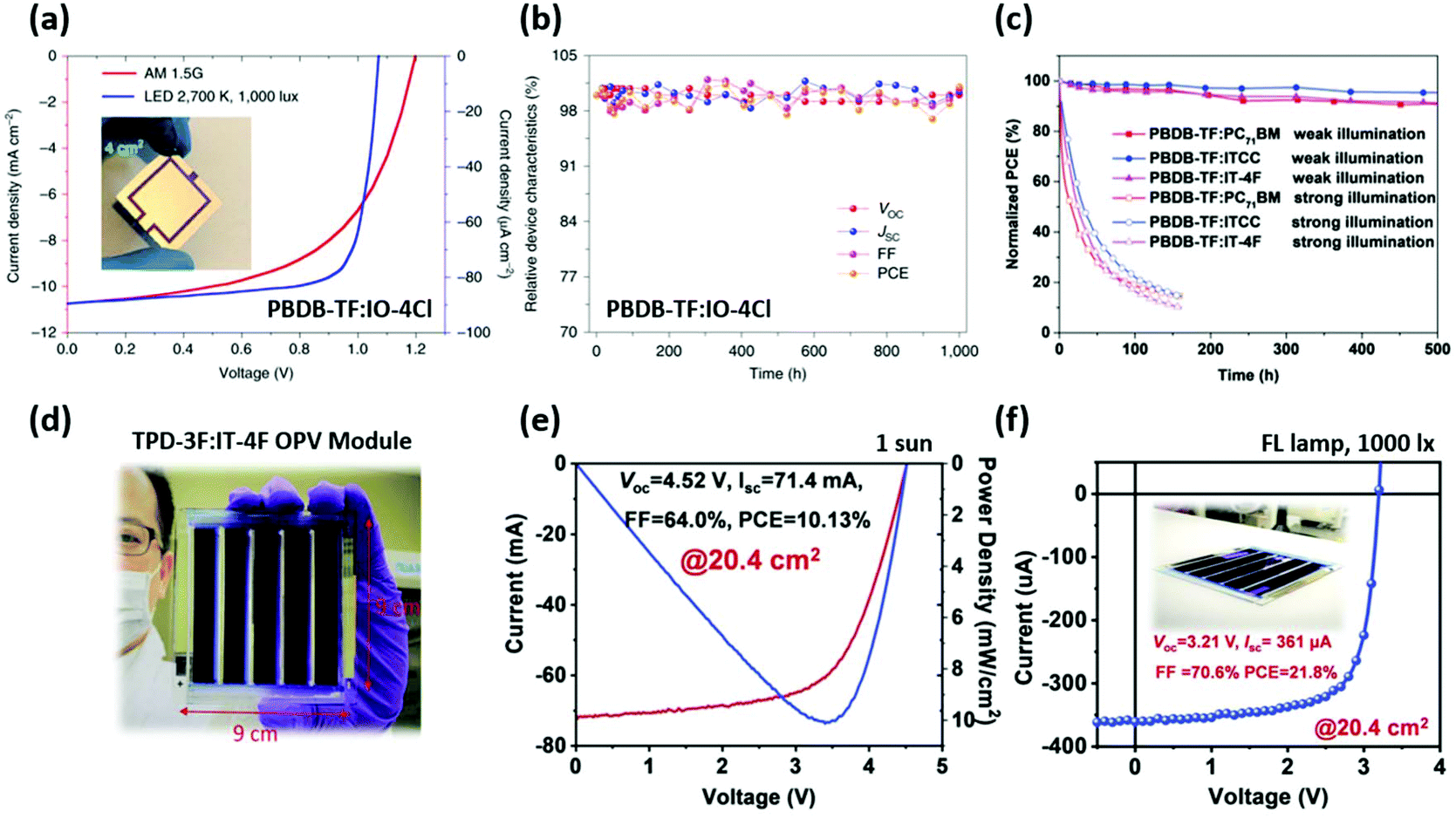 | ||
| Fig. 8 Stable large-area indoor OPVs. (a) J–V characteristics of PBDB-TF:IO-4Cl devices (device area = 4 cm2) under 1 sun and LED illumination. (b) Stability results of photovoltaic parameters versus time. Reproduced from ref. 32 with permission from Springer Nature. (c) Device stability of PBDB-TF blends with PC71BM, ITCC and IT-4F under weak and strong illumination. Reproduced from ref. 63 with permission from WILEY-VCH. Indoor OPV modules. (d) Photograph of OPV modules. (e and f) J–V characteristics of TPD-3F:IT-4F-based OPV modules under AM 1.5G and FL lamp (1000 lx) illumination, respectively. Reproduced from ref. 64 with permission from Elsevier. | ||
The indoor photovoltaic modules, which are composed of series-connected unit cells, have great potential because of the minor effect of series resistances under low light intensity. As we discussed in section 2.1, PCDTBT:PC71BM based modules (with a total active area of 100 cm2) were successfully demonstrated with a PCE of 11.2% and a Pmax of 938 μW under the FL lamp (300 lx).21 Arai et al. reported BDT-2T-ID:PNP-based OPV modules with a total active layer of 9.5 cm2 (series-connected six single cells with 1.6 cm2 area) and an outstanding maximum power output of 111 μW (PCE ∼ 15%) was obtained with a high VOC of 4.2–4.3 V under a 200 lx LED lamp.27 With the same acceptor (PNP) and a different small molecule donor (1DTP-ID), an OPV module (total active layer area: 9.6 cm2 on flexible PET substrates) also showed a high PCE of ∼17% with a power output of 95.4 μW under 200 lx (2900 K) LED illumination.28 Furthermore, over 20% module efficiency under a 1000 lx FL lamp was successfully demonstrated by Liao and coworkers.64 TPD-3F:IT-4F showed a PCE of 13.8% in single cells (JSC of 20.5 mA cm−2, VOC of 0.91 V and FF of 0.74) under 1 sun. Based on this BHJ system, they achieved module efficiencies of 10.1% under 1 sun and 21.8% under a 1000 lx FL lamp in a total active area of 20.4 cm2 (detailed photovoltaic parameters are shown in Fig. 8(e) and (f)). The overall photovoltaic parameters of the large-area cells and modules are summarized in Table 4. These are good examples of indoor OPVs with outstanding PCEs and device stability.
| Donor:acceptor |
Device area [cm2] (cells or modules) | Light source | V OC [V] | J SC [μA cm−2] | FF [%] | PCE [%] | P out [μW cm−2] | Ref. |
|---|---|---|---|---|---|---|---|---|
| a Note that these values are total short-circuit currents and output powers without considering the device area. b Only approximate PCEs are shown in these cases. c An exact value of the FF was not stated in this reference. This is an estimated value based on the other photovoltaic parameters in the paper. | ||||||||
| PBDB-TF:IO-4Cl | 4 (cells) | LED (200 lx) | 1.02 | 18.3 | 74.3 | 23.0 | 13.9 | 32 |
| PBDB-TF:IO-4Cl | 4 (cells) | LED (1000 lx) | 1.07 | 89.5 | 75.3 | 23.9 | 72.1 | 32 |
| PBDB-TF:PC71BM | 1 (cells) | LED (1000 lx) | 0.78 | 94.1 | 74.1 | 18.1 | 54.7 | 63 |
| PBDB-TF:IT-4F | 1 (cells) | LED (1000 lx) | 0.71 | 113 | 78.0 | 20.8 | 62.8 | 63 |
| PBDB-TF:ITCC | 1 (cells) | LED (1000 lx) | 0.96 | 95.8 | 72.2 | 22.0 | 66.5 | 63 |
| PCDTBT:PC71BM | 100 (modules) | FL (300 lx) | 4.87 | 314 μAa | 61.2 | 11.2 | 938 μWa | 21 |
| BDT-2T-1D:PNP | 9.5 (modules) | LED (200 lx) | 4.20 | 39.9 μAa | 66.0 | ∼15b | 111 μWa | 27 |
| 1DTP-ID:PNP | 9.6 (modules) | LED (200 lx) | 4.05 | 35.1 μAa | ∼66.0c | ∼17b | 95.4 μWa | 28 |
| TPD-3F:IT-4F | 20.4 (modules) | FL (1000 lx) | 3.21 | 361 | 70.6 | 21.8 | 40.2 | 64 |
4. Summary and outlook
In summary, ambient indoor lightings can provide sufficient energy for operating various small scale and low-power consumption indoor electronic devices. Indoor OPVs still have room for further improvement with enhanced PCEs, as the theoretical maximum efficiency at Eg = 1.90–2.20 eV was calculated to be ∼50% under FL lamps and LEDs. The band gap of photoactive materials should be fine-modulated to be well matched with specific indoor light sources, and high-VOC D:A combinations should be explored to reduce energy loss under indoor lights. From a device perspective, a high Rsh is essential for highly performing indoor OPVs. Increasing the thickness of the active layer or the charge transport layer (such as PEIE) has been reported to be an effective strategy to increase Rsh with minimized leakage currents. The molecular structure of high Rsh photoactive materials is not clear at the present stage. Further studies on the structure–property relationship are necessary to reveal the controlling factors to enhance the Rsh. In addition, because the Rs effect is not significant in indoor OPVs, low-conductivity charge transport layers also work well as ‘electrodes’, suggesting a broad window for indoor transparent electrodes. Although efficient indoor OPV modules have been successfully demonstrated, showing better stability under indoor lights compared to 1 sun illumination,32,64 systematic investigations to further improve the device stability are necessary for real applications of OPVs as semi-permanent indoor power-supply systems. Further studies on indoor OPVs should be also focused on practical applications (such as large-area, flexible, and semi-transparent devices including modules) to find real industrial markets. Another important issue is finding ways to standardize the photovoltaic characterization methods under indoor conditions. Currently light sources, irradiance intensity, and measurement conditions are all different among different research groups, making it difficult to compare or evaluate the experimental results. Similarly, with photovoltaic characterization under AM 1.5G, standard procedures are necessary to measure accurately the indoor photovoltaic characteristics for different indoor light sources.
Conflicts of interest
There are no conflicts to declare.Acknowledgements
This work was supported by the National Research Foundation (NRF) of Korea (Grants NRF-2019R1A2C2085290 and 2019R1A6A1A11044070) and the Technology Development Program to Solve Climate Changes of the NRF funded by the Ministry of Science, ICT & Future Planning (NRF-2016M1A2A2940914 and 2015M1A2A2057506).References
- G. Zhang, J. Zhao, P. C. Y. Chow, K. Jiang, J. Zhang, Z. Zhu, J. Zhang, F. Huang and H. Yan, Chem. Rev., 2018, 118, 3447–3507 CrossRef CAS PubMed.
- L. Meng, Y. Zhang, X. Wan, C. Li, X. Zhang, Y. Wang, X. Ke, Z. Xiao, L. Ding, R. Xia, H.-L. Yip, Y. Cao and Y. Chen, Science, 2018, 361, 1094–1098 CrossRef CAS PubMed.
- J. Yuan, Y. Zhang, L. Zhou, G. Zhang, H.-L. Yip, T.-K. Lau, X. Lu, C. Zhu, H. Peng, P. A. Johnson, M. Leclerc, Y. Cao, J. Ulanski, Y. Li and Y. Zou, Joule, 2019, 3, 1140–1151 CrossRef CAS.
- Y. Lin, B. Adilbekova, Y. Firdaus, E. Yengel, H. Faber, M. Sajjad, X. Zheng, E. Yarali, A. Seitkhan, O. M. Bakr, A. El-Labban, U. Schwingenschlögl, V. Tung, I. McCulloch, F. Laquai and T. D. Anthopoulos, Adv. Mater., 2019, 31, 1902965 CrossRef CAS PubMed.
- Q. Liu, Y. Jiang, K. Jin, J. Qin, J. Xu, W. Li, J. Xiong, J. Liu, Z. Xiao, K. Sun, S. Yang, X. Zhang and L. Ding, Sci. Bull., 2020, 65, 272–275 CrossRef.
- I. Mathews, S. N. Kantareddy, T. Buonassisi and I. M. Peters, Joule, 2019, 3, 1415–1426 CrossRef CAS.
- W. S. Wang, T. O'Donnell, N. Wang, M. Hayes, B. O'Flynn and C. O'Mathuna, ACM J. Emerg. Tech. Com., 2010, 6, 1 CrossRef.
- A. Nasiri, S. A. Zabalawi and G. Mandic, IEEE Trans. Ind. Electron., 2009, 56, 4502–4509 Search PubMed.
- C. Battaglia, A. Cuevas and S. D. Wolf, Energy Environ. Sci., 2016, 9, 1552 RSC.
- G. Li, R. Zhu and Y. Yang, Nat. Photonics, 2012, 6, 153 CrossRef CAS.
- J. Hou, O. Inganäs, R. H. Friend and F. Gao, Nat. Mater., 2018, 17, 119 CrossRef CAS PubMed.
- S. Kim, M. Jahandar, J. H. Jeong and D. C. Lim, Curr. Altern. Energy, 2018, 2, 1–15 CrossRef.
- F. C. Chen, Adv. Opt. Mater., 2019, 7, 1800662 CrossRef.
- N. Yana, C. Zhaoa, S. Youa, Y. Zhanga and W. Li, Chin. Chem. Lett., 2019 DOI:10.1016/j.cclet.2019.08.022.
- M. Freunek, M. Freunek and L. M. Reindl, IEEE J. Photovolt., 2013, 3, 59–64 Search PubMed.
- M. Freunek, M. Freunek and L. M. Reindl, IEEE J. Photovolt., 2013, 3, 1464–1464 Search PubMed.
- W. Shockley and H. J. Queisser, J. Appl. Phys., 1961, 32, 510–519 CrossRef CAS.
- Research Cell Record Efficiency Chart, https://www.nrel.gov/pv/assets/images/efficiency-chart.png, (accessed November 2019).
- S. Mori, T. Gotanda, Y. Nakano, M. Saito, K. Todori and M. Hosoya, Jpn. J. Appl. Phys., 2015, 54, 071602 CrossRef.
- C. L. Cutting, M. Bag and D. Venkataraman, J. Mater. Chem. C, 2016, 4, 10367–10370 RSC.
- H. K. H. Lee, Z. Li, J. R. Durrant and W. C. Tsoi, Appl. Phys. Lett., 2016, 108, 253301 CrossRef.
- Y.-J. You, C. E. Song, Q. V. Hoang, Y. Kang, J. S. Goo, D.-H. Ko, J.-J. Lee, W. S. Shin and J. W. Shim, Adv. Funct. Mater., 2019, 29, 1901171 CrossRef.
- C.-H. Chen, H.-C. Ting, Y.-Z. Li, Y.-C. Lo, P.-H. Sher, J.-K. Wang, T.-L. Chiu, C.-F. Lin, I. S. Hsu, J.-H. Lee, S.-W. Liu and K.-T. Wong, ACS Appl. Mater. Interfaces, 2019, 11, 8337–8349 CrossRef CAS PubMed.
- R. Singh, C. L. Chochos, V. G. Gregoriou, A. D. Nega, M. Kim, M. Kumar, S.-C. Shin, S. H. Kim, J. W. Shim and J.-J. Lee, ACS Appl. Mater. Interfaces, 2019, 11, 36905–36916 CrossRef CAS.
- H. Yin, S. Chen, S. H. Cheung, H. W. Li, Y. Xie, S. W. Tsang, X. Zhu and S. K. So, J. Mater. Chem. C, 2018, 6, 9111–9118 RSC.
- S.-S. Yang, Z.-C. Hsieh, M. L. Keshtov, G. D. Sharma and F.-C. Chen, Sol. RRL, 2017, 1, 1700174 CrossRef.
- R. Arai, S. Furukawa, Y. Hidaka, H. Komiyama and T. Yasuda, ACS Appl. Mater. Interfaces, 2019, 11, 9259–9264 CrossRef CAS PubMed.
- R. Arai, S. Furukawa, N. Sato and T. Yasuda, J. Mater. Chem. A, 2019, 7, 20187–20192 RSC.
- H. K. H. Lee, J. Wu, J. Barbé, S. M. Jain, S. Wood, E. M. Speller, Z. Li, F. A. Castro, J. R. Durrant and W. C. Tsoi, J. Mater. Chem. A, 2018, 6, 5618–5626 RSC.
- S. V. Dayneko, M. Pahlevani and G. C. Welch, ACS Appl. Mater. Interfaces, 2019, 11, 46017–46025 CrossRef CAS PubMed.
- Z. Ding, R. Zhao, Y. Yu and J. Liu, J. Mater. Chem. A, 2019, 7, 26533–26539 RSC.
- Y. Cui, Y. Wang, J. Bergqvist, H. Yao, Y. Xu, B. Gao, C. Yang, S. Zhang, O. Inganäs, F. Gao and J. Hou, Nat. Energy, 2019, 4, 768–775 CrossRef CAS.
- H. S. Ryu and H. Y. Woo, Sci. China: Chem., 2020, 63, 1–2 CrossRef.
- H. Yin, J. K. W. Ho, S. H. Cheung, R. J. Yan, K. L. Chiu, X. Hao and S. K. So, J. Mater. Chem. A, 2018, 6, 8579–8585 RSC.
- R. Singh, S.-C. Shin, H. Lee, M. Kim, J. W. Shim, K. Cho and J.-J. Lee, Chem. – Eur. J., 2019, 25, 6154–6161 CrossRef CAS PubMed.
- M. Nam, H. Y. Noh, J. Cho, Y. Park, S.-C. Shin, J.-A. Kim, J. Kim, H. H. Lee, J. W. Shim and D.-H. Ko, Adv. Funct. Mater., 2019, 29, 1900154 CrossRef.
- M. Nam, H. Y. Noh, J.-H. Kang, J. Cho, B. K. Min, J. W. Shim and D.-H. Ko, Nano Energy, 2019, 58, 652–659 CrossRef CAS.
- S. Y. Park, Y. Li, J. Kim, T. H. Lee, B. Walker, H. Y. Woo and J. Y. Kim, ACS Appl. Mater. Interfaces, 2018, 10, 3885–3894 CrossRef CAS PubMed.
- R. Steim, T. Ameri, P. Schilinsky, C. Waldauf, G. Dennler, M. Scharber and C. J. Brabec, Sol. Energy Mater. Sol. Cells, 2011, 95, 3256–3261 CrossRef CAS.
- P. W. M. Blom, V. D. Mihailetchi, L. J. A. Koster and D. E. Markov, Adv. Mater., 2007, 19, 1551–1566 CrossRef CAS.
- L. Hong, H. Yao, Z. Wu, Y. Cui, T. Zhang, Y. Xu, R. Yu, Q. Liao, B. Gao, K. Xian, H. Y. Woo, Z. Ge and J. Hou, Adv. Mater., 2019, 31, 1903441 CrossRef PubMed.
- K. Li, Y. Wu, Y. Tang, M.-A. Pan, W. Ma, H. Fu, C. Zhan and J. Yao, Adv. Energy Mater., 2019, 9, 1901728 CrossRef.
- Y. Lin, B. Adilbekova, Y. Firdaus, E. Yengel, H. Faber, M. Sajjad, X. Zheng, E. Yarali, A. Seitkhan, O. M. Bakr, A. El-Labban, U. Schwingenschlögl, V. Tung, I. McCulloch, F. Laquai and T. D. Anthopoulos, Adv. Mater., 2019, 31, 1902965 CrossRef CAS PubMed.
- J. Yuan, Y. Zhang, L. Zhou, G. Zhang, H.-L. Yip, T.-K. Lau, X. Lu, C. Zhu, H. Peng, P. A. Johnson, M. Leclerc, Y. Cao, J. Ulanski, Y. Li and Y. Zou, Joule, 2019, 3, 1140–1151 CrossRef CAS.
- C. E. Small, S.-W. Tsang, S. Chen, S. Baek, C. M. Amb, J. Subbiah, J. R. Reynolds and F. So, Adv. Energy Mater., 2013, 3, 909–916 CrossRef CAS.
- P. Vincent, S.-C. Shin, J. S. Goo, Y.-J. You, B. Cho, S. Lee, D.-W. Lee, S. R. Kwon, K.-B. Chung, J.-J. Lee, J.-H. Bae, J. W. Shim and H. Kim, Dyes Pigm., 2018, 159, 306–313 CrossRef CAS.
- S.-C. Shin, C. W. Koh, P. Vincent, J. S. Goo, J.-H. Bae, J.-J. Lee, C. Shin, H. Kim, H. Y. Woo and J. W. Shim, Nano Energy, 2019, 58, 466–475 CrossRef CAS.
- S.-J. Ko, B. Walker, T. L. Nguyen, H. Choi, J. Seifter, M. A. Uddin, T. Kim, S. Kim, J. Heo, G.-H. Kim, S. Cho, A. J. Heeger, H. Y. Woo and J. Y. Kim, Adv. Funct. Mater., 2016, 26, 3324–3330 CrossRef CAS.
- T. L. Nguyen, H. Choi, S. J. Ko, M. A. Uddin, B. Walker, S. Yum, J. E. Jeong, M. H. Yun, T. J. Shin, S. Hwang, J. Y. Kim and H. Y. Woo, Energy Environ. Sci., 2014, 7, 3040–3051 RSC.
- B. Kippelen and J.-L. Brédas, Energy Environ. Sci., 2009, 2, 251–261 RSC.
- B. P. Lechêne, M. Cowell, A. Pierre, J. W. Evans, P. K. Wright and A. C. Arias, Nano Energy, 2016, 26, 631–640 CrossRef.
- J. S. Goo, S.-C. Shin, Y.-J. You and J. W. Shim, Sol. Energy Mater. Sol. Cells, 2018, 184, 31–37 CrossRef CAS.
- S.-C. Shin, Y.-J. You, J. S. Goo and J. W. Shim, Appl. Surf. Sci., 2019, 495, 143556 CrossRef CAS.
- J. S. Goo, J.-H. Lee, S.-C. Shin, J.-S. Park and J. W. Shim, J. Mater. Chem. A, 2018, 6, 23464–23472 RSC.
- W. Cao, Y. Zheng, Z. Li, E. Wrzesniewski, W. T. Hammond and J. Xue, Org. Electron., 2012, 13, 2221–2228 CrossRef CAS.
- D. C. Lim, J. H. Jeong, K. Hong, S. Nho, J.-Y. Lee, Q. V. Hoang, S. K. Lee, K. Pyo, D. Lee and S. Cho, Prog. Photovoltaics, 2018, 26, 188–195 CAS.
- G. Sun, M. Shahid, Z. Fei, S. Xu, F. D. Eisner, T. D. Anthopolous, M. A. McLachlan and M. Heeney, Mater. Chem. Front., 2019, 3, 450–455 RSC.
- B. R. Lee, J. S. Goo, Y. W. Kim, Y.-J. You, H. Kim, S.-K. Lee, J. W. Shim and T. G. Kim, J. Power Sources, 2019, 417, 61–69 CrossRef CAS.
- H. Choi, S.-J. Ko, Y. Choi, P. Joo, T. Kim, B. R. Lee, J.-W. Jung, H. J. Choi, M. Cha, J.-R. Jeong, I.-W. Hwang, M. H. Song, B.-S. Kim and J. Y. Kim, Nat. Photonics, 2013, 7, 732–738 CrossRef CAS.
- S. Song, J. Heo, T. K. Lee, S. Park, B. Walker, S. K. Kwak and J. Y. Kim, J. Phys. Chem. C, 2017, 121, 17569–17576 CrossRef CAS.
- X. Li, W. C. H. Choy, H. Lu, W. E. I. Sha and A. H. P. Ho, Adv. Funct. Mater., 2013, 23, 2728–2735 CrossRef CAS.
- N.-W. Teng, S.-S. Yang and F.-C. Chen, IEEE J. Photovolt., 2018, 8, 752–756 Search PubMed.
- Y. Cui, H. Yao, T. Zhang, L. Hong, B. Gao, K. Xian, J. Qin and J. Hou, Adv. Mater., 2019, 31, 1904512 CrossRef CAS PubMed.
- C.-Y. Liao, Y. Chen, C.-C. Lee, G. Wang, N.-W. Teng, C.-H. Lee, W.-L. Li, Y.-K. Chen, C.-H. Li, H.-L. Ho, P. H.-S. Tan, B. Wang, Y.-C. Huang, R. M. Young, M. R. Wasielewski, T. J. Marks, Y.-M. Chang and A. Facchetti, Joule, 2019, 4, 189–206 CrossRef.
Footnote |
| † These authors contributed equally to this work. |
| This journal is © The Royal Society of Chemistry 2020 |