
 Open Access Article
 This Open Access Article is licensed under a
 Creative Commons Attribution 3.0 Unported Licence
Glow discharge optical emission spectrometry for quantitative depth profiling of CIGS thin-films†
Tim
Kodalle
 *a,
Dieter
Greiner
a,
Varvara
Brackmann‡
b,
Karsten
Prietzel
a,
Anja
Scheu
a,
Tobias
Bertram
a,
Pablo
Reyes-Figueroa
a,
Thomas
Unold
a,
Daniel
Abou-Ras
a,
Rutger
Schlatmann
ac,
Christian A.
Kaufmann
a and
Volker
Hoffmann
b
*a,
Dieter
Greiner
a,
Varvara
Brackmann‡
b,
Karsten
Prietzel
a,
Anja
Scheu
a,
Tobias
Bertram
a,
Pablo
Reyes-Figueroa
a,
Thomas
Unold
a,
Daniel
Abou-Ras
a,
Rutger
Schlatmann
ac,
Christian A.
Kaufmann
a and
Volker
Hoffmann
b
aHelmholtz-Zentrum Berlin für Materialien und Energie GmbH, Hahn-Meitner Platz 1, D-14109, Berlin, Germany. E-mail: tim.kodalle@helmholtz-berlin.de
bIFW Dresden, Institute for Complex Materials, Helmholtzstraße 20, D-01069 Dresden, Germany
cHochschule für Technik und Wirtschaft Berlin, Treskowallee 8, 10318 Berlin, Germany
First published on 11th April 2019
Abstract
Determining elemental distributions dependent on the thickness of a sample is of utmost importance for process optimization in different fields e.g. from quality control in the steel industry to controlling doping profiles in semiconductor labs. Glow discharge optical emission spectrometry (GD-OES) is a widely used tool for fast measurements of depth profiles. In order to be able to draw profound conclusions from GD-OES profiles, one has to optimize the measurement conditions for the given application as well as to ensure the suitability of the used emission lines. Furthermore a quantification algorithm has to be implemented to convert the measured properties (intensity of the emission lines versus sputtering time) to more useful parameters, e.g. the molar fractions versus sample depth (depth profiles). In this contribution a typical optimization procedure of the sputtering parameters is adapted to the case of polycrystalline Cu(In,Ga)(S,Se)2 thin films, which are used as absorber layers in solar cell devices, for the first time. All emission lines used are shown to be suitable for the quantification of the depth profiles and a quantification routine based on the assumption of constant emission yield is used. The accuracy of this quantification method is demonstrated on the basis of several examples. The bandgap energy profile of the compound semiconductor, as determined by the elemental distributions, is compared to optical measurements. The depth profiles of Na – the main dopant in these compounds – are correlated with measurements of the open-circuit voltage of the corresponding devices, and the quantification of the sample depth is validated by comparison with profilometry and X-ray fluorescence measurements.
Introduction
Solar cells based on Cu(In,Ga)(Se,S)2 (CIGSSe) absorber layers exhibit the highest power conversion efficiencies (PCE) of all polycrystalline thin film technologies,1 which makes this type of solar cell a promising candidate for managing the challenge of clean electric energy supply in the future. To achieve PCEs as high as the current world record of 22.9%,2 it is crucial to adjust the bandgap energy (Eg) profile and the gradients of the quasi-fermi levels within the CIGSSe absorber layer.2–4 To do so, one has to adjust the in-depth elemental gradient of In and Ga as well as Se and S in the compound semiconductor carefully.5 Typically a double-graded Eg-structure is used to achieve the highest PCEs. The minimum Eg is adapted to the spectrum of the sunlight according to the Shockley-Queisser-limit,6 while Eg increases towards the interfaces at the front- and the back-contact. By achieving a higher Eg at these interfaces, the recombination velocity there can be reduced.7,8 Furthermore one can optimize the offset of the conduction bands of the absorber layer and the neighbouring buffer layer at the front interface. Depending on the deposition process such an Eg-profile can be achieved by adjusting the ratios of the molar fraction of Ga and In (χGa/(χGa + χIn) = GGI) within a S-free Cu(In,Ga)Se2 (CIGSe) absorber layer.9 But when using e.g. a sequential deposition process based on a rapid thermal processing (RTP-) step of metal precursors in a chalcogen atmosphere, there is no direct control of the GGI and one needs to adjust the Eg-gradient towards the front interface by the additional incorporation of S into CIGSe. Therefore one has to adjust the molar fractions of the anions accordingly (χS/(χS + χSe) = SSSe).8Pulsed glow discharge optical emission spectroscopy (GD-OES) is a fast and well-suited technique to measure the elemental distribution with sufficient depth resolution in the 2–3 μm thick CIG(S)Se layers.10 Although GD-OES cannot achieve similar limits of detection to its counterparts based on mass spectrometry (MS), it is sensitive enough to obtain sufficiently good depth profiles of the main components of CIGSSe as well as of the main dopants. Additionally GD-OES is faster, cheaper and easier to perform than for example glow discharge mass spectrometry (GD-MS) or secondary ion mass spectrometry (SIMS), mainly because it does not require ultrahigh vacuum. Mild surface sputtering and fast sampling time of commercial light detection systems therefore make GD-OES a competitive and fast method for depth profiling of thin layers (few nm to more than 100 μm). For a more comprehensive comparison of GD-OES with various other depth profiling techniques the reader is referred to a previous study published by Abou-Ras et al.10
Since the measured raw data of a GD-OES depth profile (intensity vs. sputtering time) are not directly suitable for an accurate analysis of e.g. the Eg-profile, a reliable quantification procedure is required to obtain the molar fractions of the contained elements as a function of the thickness of the absorber layer. Although GD-OES is already widely used for obtaining depth profiles of CIGSSe thin films,11–18 to the best of our knowledge there is no study published yet to test its overall applicability and the specific suitability of the used atomic transitions of the elements contained in CIGS for this purpose.
In the present contribution we demonstrate how to optimize the glow discharge conditions for accurate measurements of CIGSSe thin films and present a quantification algorithm based on the main assumption of constant emission yields adapted to these types of samples.19 Furthermore we test the used emission lines for their usability in this quantification and evaluate the resulting quantified depth profiles for several applications.
Experimental
Sample preparation
The CIGSe-layers used as reference samples are deposited on soda-lime glass covered by 800 nm Mo. The CIGSe layer is grown by single stage co-evaporation of the contained elements onto the heated substrates in a vacuum based deposition process. Details of the utilized setup can be found in ref. 20. The CuInS2 sample used for calibration was deposited in a similar process using a different system.21 A cold-pressed CIGSSe:Na-reference sample was used for the quantification of S and Na. The cylindrical sample with a diameter and a thickness of 2 cm each was provided by Evochem Advanced Materials GmbH. For calibration purposes, certified cast Cu:S samples as well as sintered Cu:NaCl were used. The sintering process is described in ref. 22. The properties of all reference and calibration samples used in this study are summarized in the ESI.† The samples used for the verification of the method (solar cell applications) are either grown in the same system as the CIGSe reference layers, but using a three-stage process (S-free samples)20 or are grown using a sequential RTP (in the case of CIGSSe-samples). Details of this RTP are published in ref. 23.Measurement techniques
All GD-OES depth profiles were measured using a GDA650-system built by Spectruma Analytik in pulsed radio frequency (rf) mode, in order to be able to sputter the semiconducting absorber layer and to avoid heat-induced damage of the glass substrate. The system uses an Ar-plasma for sputtering and a CCD-array to detect the photons emitted during the relaxation of the atoms and ions, which were detached from the matrix and excited in the plasma. For the rf mode, the system is equipped with a Grimm-type glow discharge source including an anode with an inner diameter of 2.5 mm and a non-conducting cathode plate with front end coupling.24 Details of the setup can be found in ref. 25 and 26.Profiles of the sputtered craters are measured using a Dektak and an FRT MicroProf profilometer. The current density–voltage (j–V) measurements were performed under standard test conditions (AM 1.5 g spectrum, 1000 W m−2, 25 °C) using a WACOM A+ solar simulator; external quantum efficiency (EQE)-measurements were carried out using a self-built setup, and X-ray fluorescence spectrometry (XRF) measurements were performed with a Rigaku ZSX Primus II.
Results and discussion
Optimization of the sputtering parameters for flat crater profiles
The depth resolution of GD-OES is limited by the formation of a nonplanar sputtered crater in the sample and sputter induced roughening of the sample surface.To reach the best possible depth resolution and to measure a reliable depth profile of the sample by means of GD-OES, it is necessary to optimize the analysis conditions, i.e. to reduce the curvature and roughness in the sputtered crater to a minimum. Hence, it is necessary to adjust the parameters of the sputtering cell accordingly, which are the voltage U, the current I, the pressure p, and in case a pulsed mode is used also the pulse length l, the frequency f, and the duty cycle.
The U, I and p, as well as duty cycle, l, and f are interdependent. To simplify the optimization work, it was assumed that p and f have a smaller effect on the shape of the sputtered crater as compared with the other parameters.25,27,28 However, in the case of rf discharge, it is hard to measure the current reliably. Therefore, in the present work the pressure is measured instead. Thus, there are four parameters to optimize: U, p, l, and the duty cycle. For a good understanding of the influence of each parameter separately, it is important to vary just one parameter at a time and keep all others constant.
By carefully optimizing all parameters according to these rules, the optimal analysis parameters for the CIGSe samples were chosen to be: p = 2.5 hPa, U = 650 V, f = 451 Hz, l = 89 μs, duty cycle: 4%. Using these parameters it takes about 5 min to sputter through one of our standard CIGSe-layers with a thickness of approx. 2.5 μm. In Fig. 1 the profile of a sputtered crater generated with these parameters and measured using the profilometer is shown. Some examples of how the profile of the sputtered crater is influenced by non-optimal sputtering parameters are shown in the ESI (Fig. SI1†).
 | ||
| Fig. 1 Profilometer scan of a sputtered crater in a Mo/CIGSe layer stack. The image shows an average of 21 line scans taken within a distance of ∼0.4 mm in the middle of the file; moderate voltage and pressure were chosen in the present study. | ||
Please note that the sputtering parameters depend on the experimental setup and should be established for each system individually, according to the aforesaid principles.
Quantification of the GD-OES depth profiles
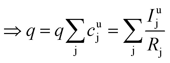
The aim of the quantification of the GD-OES profiles is to derive profiles of the molar fraction of each element vs. the layer depth from the measured intensity vs. sputtering time.To do so an algorithm based on the assumption of constant emission yield is used.19 The emission yield Rj for atoms of element j is defined as the number of photons emitted per atom of this element removed from the sample's surface. Rj is one of the proportionality factors between the measured intensity Ij of element j – or more precisely the intensity of a chosen emission line transition of this element – and the actual mass fraction cj of this element in the matrix. The other proportionality factors are the sputtering rate q and the instrumental detection efficiency kj. The factor Sj takes self-absorption into account and becomes a function of cjq, which is smaller than 1, if emitted photons are absorbed after emission. Additionally Ij depends on a background value bj determined by the used instrument:27
| Ij = kjSjRjcjq + bj | (1) |
By measuring the intensities of reference samples with known cj and q, one can transform measured intensities from unknown samples into their mass fractions using eqn (1). To do so one has to account for the background of the given emission line e.g. by choosing lines with a background that is small compared to the actual intensities or by measuring and subtracting bj. Secondly one has to determine whether the intensity of the used emission line is linearly dependent on the introduced mass of element j per time in the plasma cjq. This information is obtained by creating calibration curves for all used emission lines. In these calibration curves usually the intensity is plotted versus the product cjq. At the intersection of these curves and the intensity-axis one can determine bj. If the curves show a linear dependence of Ij on cjq, self-absorption can be neglected and Sj becomes 1.
Furthermore it is assumed that kj is independent of the measured sample and the sputtering parameters, but is a constant only dependent on the utilized spectrometer. For all used emission lines this instrumental factor is included in Rj. Therefore, for the calculation of cjq of unknown samples from the measured line intensities, eqn (1) is actually used in a simplified form, if calibration shows linearity in the region of interest
| Ij = Rjcjq + bj | (2) |
| Ij = Rjcjq | (3) |
 | (4) |
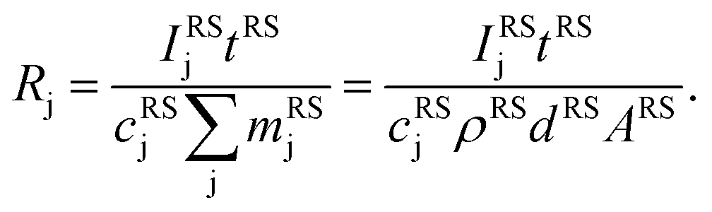
Here we used the sputtering rate given by the fraction of the sputtered mass of all contained elements 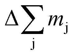 per sputtering time Δt. When reference samples with a homogeneous distribution of all elements within the layer are used, one can integrate over all sputtering times Δt and conclude for the whole layer:
 | (5) |
Since it is difficult to measure the sputtered mass with high accuracy, one has to use the product of the sample density ρ and its volume V, which in the case of a reference layer is given by the thickness d of the sputtered layer and the area of the sputtered crater A. For bulk calibration materials the density also has to be known and the sputtered mass can then be calculated from the measured crater volume.31
 | (6) |
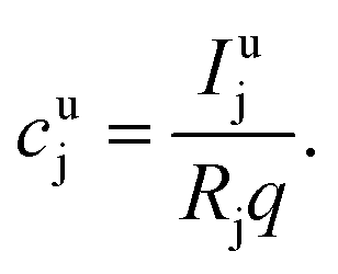
As long as the matrix of the unknown sample is the same as the matrix of the reference sample the sputtering rate determined from the reference sample can also be used for the quantification of the unknown sample. However, in reality the unknown measurement samples commonly show different concentrations of the contained elements as well as gradients of these over the sample depth. Therefore in most cases the sputtering rate has to be determined for each sputtering cycle of the measurement of the unknown sample. To do so, it is assumed that the sum of the mass concentration as well as the molar fractions of all measured elements equals 1 (for this reason it is important to note that the quantification can only be performed, if nearly 100% of the elements present are determined):
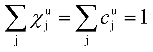 | (7) |
 | (8) |
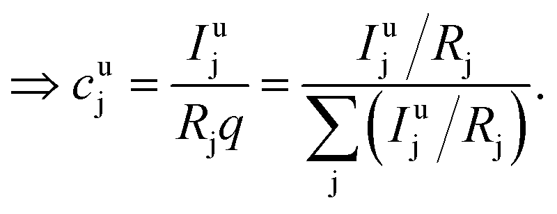 | (9) |
This can be done for each measurement step, i.e. for each time slice of the measurement. In a last step the molar fraction of each element and time slice can be calculated from the mass fraction using the atomic mass of each element j (Mj):
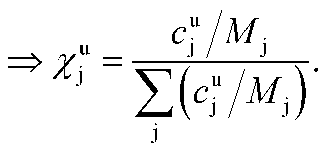 | (10) |
In the first approach it is assumed that each layer, which is sputtered from the sample during one sputtering cycle, consists of the sum of hypothetical layers of the contained elements, e.g. a CIGSe-layer is replaced by a stack of Cu, In, Ga and Se. With that assumption one can calculate the thickness of this layer by determining the hypothetical layer thickness for each element j, which is sputtered from the sample during each sputtering cycle Δt:
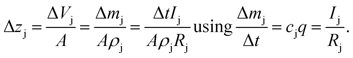 | (11) |
This estimation uses the densities ρj of the pure elements. The actual sputtering depth can then be derived by summing up the individual layer thicknesses of all elements:
 | (12) |
This assumption is valid for metals and alloys,28 but can lead to some errors in other materials. As an example the densities for C in graphite (2.26 g cm−3) and diamond (3.52 g cm−3) differ remarkably, which shows that the use of just one density of C can lead to substantial errors.
Another approach therefore is to replace the elemental densities with the actual density of the sputtered layer, e.g. the CIGSe with the exact composition during that sputtering cycle:
 | (13) |
For each sputtering cycle the density of the CIGSe can be calculated by the following formula based on Vegard's law,32 assuming a constant Cu-content:
 | (14) |
Here, the index “UC” marks properties of the unit cell. Furthermore nj is the number of atoms of element j per unit cell, and a and c are the lattice parameters of the chalcopyrite's unit cell. According to Vegard's law the lattice parameters of the CIGSe (a,c)CIGSe can be calculated using the lattice parameters of the two constituents CuInSe2 (a,c)CISe and CuGaSe2 (a,c)CGSe weighted by the GGI.32
Additionally the lattice parameters are dependent on the CGI (CGI = χCu/(χGa + χIn)), but since this dependency is mostly determined by the formation of Cu-related defects in the crystal structure, there is no generally valid expression derived yet.33,34 However, for a given CGI the lattice parameters can be derived experimentally – and do not depend on CGI strongly33,34 in the range usually used for highly efficient CIGSSe solar cells (0.85 < CGI < 0.95).13 Stephan et al.34 showed that the volume of the unit cell of CISe within that CGI-range is altered by not more than 0.07%. However, one has to keep in mind that the error might become relevant at very low CGI.
In Table 1 the layer thickness of seven standard CIGSe layers (with Ga-grading, cf. examples section) as determined using a profilometer (dDektak) is shown and the deviation of the thickness from that value determined by XRF (dXRF) and GD-OES using both methods described above is displayed. In the latter measurements the depth at which the Mo-signal reaches χMo = 0.1 was chosen as the end of the CIGSe-layer. In all cases the thickness, which was determined using eqn (13) and (14), i.e. ΔdCIGSGD-OES, is slightly higher than the one determined following eqn (11) and (12), i.e. ΔdelementalGD-OES. All three methods show sufficiently small deviation in the range of the error of the profilometer itself confirming that the approach of combining the elemental densities is valid for CIGSe thin films.
| ID | d Dektak (μm) | ΔdXRF | ΔdelementalGD-OES | ΔdCIGSGD-OES |
|---|---|---|---|---|
| 1 | 2.22 ± 0.06 | 6.2% | 1.6% | 4.5% |
| 2 | 2.28 ± 0.03 | 3.5% | −0.9% | 2.2% |
| 3 | 2.30 ± 0.05 | 5.6% | −2.30% | 0.9% |
| 4 | 2.38 ± 0.02 | 1.6% | −1.1% | 1.1% |
| 5 | 2.40 ± 0.01 | 0.8% | −3.7% | −0.7% |
| 6 | 2.40 ± 0.03 | 1.3% | −4.6% | −1.7% |
| 7 | 2.51 ± 0.03 | 1.1% | −4.3% | −1.1% |
| Average | 2.9% | −2.2% | 0.7% |
Calibration curves
In order to obtain optimum Eg-gradients, the composition of the CIGSSe can be changed drastically within one absorber layer. In standard high efficiency CIGSe solar cells (S free) GGI ranges from about GGI ≈ 0.2 at the minimum Eg up to values of GGI ≈ 0.6 at the rear interface CIGSe/Mo. Similar – though not as pronounced – changes of the concentration of Cu and Se occur near the front interface. Furthermore the concentration of S in CIGSSe samples usually ranges from SSSe ≈ 0.1 to SSSe ≈ 0.5, while the molar fraction of Na lies in the order of magnitude of χNa = 1 × 10⁻⁴.In order to be able to apply the quantification routine to these layers, one has to ensure two things:
(1) Self-absorption Sj can be neglected.
(2) The background bj is either negligible or is measured and subtracted from the measured intensity in an additional step prior to the described quantification. Only then the emission yield determined at one given concentration of each element can be used to quantify the measurement at all concentrations, i.e.eqn (1) can be simplified to eqn (3).
Gradient-free CIGSe reference samples with different CGI and GGI were grown and characterized in order to test these two conditions for Cu, Se, In, and Ga. Additional calibration samples were used to do so for S and Na. In Fig. 2(a) to (f) the calibration curves of the used elemental transitions of Cu, Se, In, Ga, S, and Na are displayed. Note that we distinguish between reference samples, which are used for both the calibration curves and the quantification of the unknown samples and therefore have the same matrix and similar composition to the latter (marked green in Fig. 2) as well as calibration samples (marked black), which are only used to generate calibration curves over a wider range. Excluding thus background and non-linearity issues, the validity of the quantification algorithm described above using just the matrix specific samples (green symbols) and no background correction is confirmed.
 | ||
| Fig. 2 Calibration curves of (a) Cu, (b) Se, (c) In, (d) Ga, (e) S, and (f) Na. Black symbols mark samples, which were only used for these calibration curves, while samples marked in green are additionally used as reference samples during the quantification. | ||
As can be seen in Fig. 2(a)–(d), the calibration curves of the used emission lines of Cu, Se, In, and Ga (Cu: 327 nm, In: 451 nm, Ga: 417 nm, Se: 196 nm) are linear and don't show any significant background at cjq = 0. Therefore we can safely neglect Sj and bj in these cases. The emission lines of S at 181 nm and the one of Na at 589 nm, however, show a more complex behaviour. The S-line does show a linear dependence on cSq, but also shows a background at cS·q = 0 of about 0.007. While this background is negligible in the case of most CIGSSe-samples (CIGSSe-samples grown in our lab exhibit S-concentrations lying within the yellow marked area in Fig. 2(e)), one has to be careful when analysing S-free samples. In the latter case one has to either exclude the S-signal completely from the quantification, which seems reasonable if there is no risk of contamination, or to manually subtract the background from the measured S-signal.
The Na-line on the other hand is not affected by any background, but shows a non-linear dependence of the measured intensity on cNaq. This saturation of the intensity at high Na-concentration is most likely due to self-absorption occurring for the used emission line. This means that photons, which are emitted by Na-atoms sputtered from the sample, don't reach the detector, because they are absorbed by Na-atoms in the region between the plasma and source window. Since this effect is exponentially dependent on the number of atoms in the volume of absorption,35 it becomes more important at higher concentrations and sputtering rates. If an emission line is strongly affected by self-absorption (this is often the case for emission lines to the ground state at so-called resonance lines) the influence of the self-absorption can also lead to a change of the line-shape of the measured peak, which has to be taken into account as well. The reader is referred to ref. 35 for further details on this issue.
However, since the data can be interpolated by a linear fit function for Na-concentrations typically found in CIGSSe solar cells (<1 × 10⁻³) with a reasonable error (see comparison of the fitting curves in Fig. 2(f)), Sj can still be neglected in our case. If analysing samples with high Na-concentrations, one would have to fit a quadratic or higher order polynomial function to quantify the Na-signal. Please note that the dependences shown in this section are only valid for the used system and sputtering parameters.
Reference samples
In order to be a suitable reference sample for a matrix specific determination of the emission yields, the sample has to meet several requirements:(1) Similar matrix to the unknown samples.
(2) Vacuum tightness to act as a sealing against the atmosphere and stability during the sputtering process.
(3) Known concentrations cj of all contained elements.
(4) Known sputtering rate.
If the layers are used for calibration:
(5) Known thickness of the complete layer.
(6) Homogeneous distribution of all contained elements throughout the layer.
(7) Known density of the layer. Requirements (1), (2) and to (6) can be easily met in the case of S-free CIGSe, since gradient-free CIGSe layers can be grown in a co-evaporation system. The cj of all contained elements and the thickness of the layer are adjusted with in situ optical process controls and are verified by XRF.36,37 The density of the layers is determined using eqn (14).
Since our co-evaporation system is not equipped with an S-source, we cannot grow reference samples for CIGSSe ourselves. Therefore a cold-pressed CIGSSe:Na sample meeting all the requirements listed above was included. In Fig. SI2 of the ESI† images of both a self-grown CIGSe and the CIGSSe:Na reference sample and the corresponding qualitative depth profiles are shown.
Since the CIGSSe:Na sample is about 2 cm thick, the reference measurement cannot be performed through the whole sample but has to be stopped manually. The depth of the sputtered crater has to be determined in an extra step. This can be done directly by measuring it with a profilometer or indirectly by comparing the emission yields of Cu, In, Ga and Se with the ones obtained from the thin film reference. In the latter case, the sputtering depth of the CIGSSe:Na sample is used as a free parameter to correlate the emission yields of Cu, In, Ga and Se measured in the CIGSSe:Na reference with the ones obtained from the thin film sample with known thickness. The result of this fit is used for the determination of the emission yields of S and Na. Na is the main dopant in CIGSSe absorber layers,38 and its depth profile can give valuable information about diffusion processes during the formation of the absorber layer. The importance of the ability to measure the Na depth profile is discussed below.
Examples of applications
| Eg = 1 + 0.564 × GGI + 0.116 × GGI2. | (15) |
In the case of CIGSSe absorber layers containing S we use the formula published by Bär et al.:40
| Eg = 1 + 0.13 × GGI2 + 0.08 × GGI2·SSSe + 0.13 × GGI·SSSe + 0.55 × GGI + 0.54SSSe. | (16) |
 | ||
| Fig. 3 (a) Quantified depth profile of a standard CIGSe layer. (b) Calculated profiles of CGI, GGI and Eg of the same layer. | ||
 | ||
| Fig. 4 Determination of the optical bandgap energy from the first derivative of the EQE of a solar cell made from a CIGSe-absorber from the same deposition run as the one for which the GD-OES profile is shown in Fig. 3. | ||
 | ||
| Fig. 5 (a) Molar fraction of Na of four different samples with different amounts of Na incorporated derived from GD-OES measurements. (b) Open-circuit voltage of the corresponding solar cells. | ||
Conclusions
In the present contribution we showed how to optimize the sputtering parameters of pulsed GD-OES for investigating the elemental depth profiles of CIGSSe thin films. After ensuring optimum sputtering conditions, one emission line for each contained element was tested for its suitability for quantitative depth profiling. We could demonstrate for the first time that the utilized emission lines of Cu, In, Ga and Se exhibit a linear dependence on the product of concentration times and sputtering rate and are therefore indeed usable for the quantification. Furthermore we demonstrated that the suitability of the emission lines of S and Na used here has to be carefully evaluated for each specific case and hence further corrections might be necessary. A quantification algorithm based on the assumption of constant emission yield is applied to the case of CIGSSe. The accuracy of the final quantified profiles of the molar fractions of each element was demonstrated by several examples. These results subsequently justify the use of GD-OES in general and the tested emission lines in particular for quantitative compositional depth profiling of CIGSSe thin films.Conflicts of interest
There are no conflicts to declare.Acknowledgements
The authors thank S. Cinque, S. Falk and J. Lauche for maintaining the GD-OES system, V. Hinrichs for performing the LA-ICP-MS measurements, C. Stephan for fruitful discussions as well as B. Bunn, M. Hartig, J. Lauche and T. Münchenberg for preparation of the substrates and absorber layers. They also thank K. Coulibaly for profilometer measurements, H. Merker and S. Donath for the preparation of sintered calibration samples, A. Lomuscio from the University of Luxembourg for the preparation of the CuInS2-thin film and C. Prinz from the Bundesanstalt fuer Materialforschung und -pruefung (BAM) for measurements of the sample density.References
- M. A. Green, Y. Hishikawa, E. D. Dunlop, D. H. Levi, J. Hohl-Ebinger and A. W. Y. Ho-Baillie, Prog. Photovoltaics, 2018, 26, 3–12 Search PubMed.
- T. Kato, J.-L. Wu, Y. Hirai, H. Sugimoto and V. Bermudez, IEEE J. Photovolt., 2018, 1–6 Search PubMed.
- W. Shockley and H. J. Queisser, J. Appl. Phys., 1961, 32, 510–519 CrossRef CAS.
- M. A. Contreras, J. Tuttle, A. M. Gabor, A. Tennant, K. Ramanathan, S. Asher, A. Franz, J. Keane, L. Wang, J. Scofield and R. Noufi, Proc. 1st WCPEC, Waikoloa, Hawaii, 1994, pp. 83–86 Search PubMed.
- S.-H. Wei and A. Zunger, J. Appl. Phys., 1995, 78, 3846–3856 CrossRef CAS.
- L. M. Peter, Philos. Trans. R. Soc., A, 2011, 369, 1840–1856 CrossRef CAS PubMed.
- T. M. Friedlmeier, P. Jackson, A. Bauer, D. Hariskos, O. Kiowski, R. Menner, R. Wuerz and M. Powalla, Thin Solid Films, 2017, 633, 13–17 CrossRef CAS.
- T. Dullweber, O. Lundberg, J. Malmström, M. Bodegard, L. Stolt, U. Rau, H. W. Schock and J. H. Werner, Thin Solid Films, 2001, 387, 11–13 CrossRef CAS.
- A. M. Gabor, J. R. Tuttle, D. S. Albin, M. A. Contreras, R. Noufi and A. M. Hermann, Appl. Phys. Lett., 1994, 65, 198–200 CrossRef CAS.
- D. Abou-Ras, R. Caballero, C.-H. Fischer, C. A. Kaufmann, I. Lauermann, R. Mainz, H. Mönig, A. Schöpke, C. Stephan, C. Streeck, S. Schorr, A. Eicke, M. Döbeli, B. Gade, J. Hinrichs, T. Nunney, H. Dijkstra, V. Hoffmann, D. Klemm, V. Efimova, A. Bergmaier, G. Dollinger, T. Wirth, W. Unger, A. A. Rockett, A. Perez-Rodriguez, J. Alvarez-Garcia, V. Izquierdo-Roca, T. Schmid, P.-P. Choi, M. Müller, F. Bertram, J. Christen, H. Khatri, R. W. Collins, S. Marsillac and I. Kötschau, Microsc. Microanal., 2011, 17, 728–751 CrossRef CAS PubMed.
- T. Delsol, A. P. Samantilleke, N. B. Chaure, P. H. Gardiner, M. Simmonds and I. M. Dharmadasa, Sol. Energy Mater. Sol. Cells, 2004, 82, 587–599 CAS.
- R. Caballero, C. A. Kaufmann, V. Efimova, T. Rissom, V. Hoffmann and H.-W. Schock, Prog. Photovoltaics, 2011, 21, 30–46 Search PubMed.
- M. Powalla, P. Jackson, W. Witte, D. Hariskos, S. Paetel, C. Tschamber and W. Wischmann, Sol. Energy Mater. Sol. Cells, 2013, 119, 51–58 CrossRef CAS.
- T. Klinkert, M. Jubault, F. Donsanti, D. Lincot and J.-F. Guillemoles, Thin Solid Films, 2014, 558, 47–53 CrossRef CAS.
- D. Mercier, M. Bouttemy, J. Vigneron, P. Chapon and A. Etcheberry, Appl. Surf. Sci., 2015, 347, 799–807 CrossRef CAS.
- P. Haunault, C. Morin, and P. Chapon, IEEE 42nd PVSC, New Orleans, Louisiana, 2015, DOI:10.1109/PVSC.2015.7356028.
- S. Zahedi-Azad and R. Scheer, Phys. Status Solidi C, 2017, 14, 1600203 Search PubMed.
- W. Zhang, H. Zhu, L. Zhang, Y. Guo, X. Niu, Z. Li, J. Chen, Q. Liu and Y. Mai, Solid-State Electron., 2017, 132, 57–63 CrossRef CAS.
- A. Bengtson and T. Nelis, Anal. Bioanal. Chem., 2006, 385, 568–585 CrossRef CAS PubMed.
- M. D. Heinemann, R. Mainz, F. Österle, H. Rodriguez-Alvarez, D. Greiner, C. A. Kaufmann and T. Unold, Sci. Rep., 2017, 7, 45463 CrossRef CAS PubMed.
- A. Lomuscio, M. Melchiorre and S. Siebentritt, IEEE 7th WCPEC, 2018, DOI:10.1109/PVSC.2018.8548252.
- C. Gonzalez-Gago, P. Smid, T. Hofmann, C. Venzago, V. Hoffmann and W. Gruner, Anal. Bioanal. Chem., 2014, 406, 7473–7482 CrossRef CAS PubMed.
- S. S. Schmidt, C. Wolf, H. Rodriguez-Alvarez, J.-P. Bäcker, C. A. Kaufmann, S. Merdes, F. Ziem, M. Hartig, S. Cinque, I. Dorbandt, C. Köble, D. Abou-Ras, R. Mainz and R. Schlatmann, Prog. Photovoltaics, 2017, 25, 341–357 CAS.
- W. Grimm, German Patent 1, 589 389, 1967.
- V. Efimova, V. Hoffmann and J. Eckert, J. Anal. At. Spectrom., 2011, 26, 784–791 RSC.
- L. Wilken, V. Hoffmann, H.-J. Uhlemann, H. Siegel and K. Wetzig, J. Anal. At. Spectrom., 2003, 18, 646–655 RSC.
- V. Efimova, PhD thesis, Technical University Dresden, 2011.
- R. Payling, Glow Discharge Optical Emission Spectrometry, John Wiley & Sons, Hoboken, New Jersey, 1997, ch. 6.4, pp. 287–291 Search PubMed.
- V. Efimova, V. Hoffmann and J. Eckert, Spectrochim. Acta, Part B, 2012, 76, 181–189 CrossRef CAS.
- D. Abou-Ras, B. Marsen, T. Rissom, F. Frost, H. Schulz, F. Bauer, V. Efimova, V. Hoffmann and A. Eicke, Micron, 2012, 43, 470–474 CrossRef CAS PubMed.
- L. Wilken, V. Hoffmann and K. Wetzig, J. Anal. At. Spectrom., 2003, 18, 1141–1145 RSC.
- L. Vegard, Z. Phys., 1921, 5, 17–26 CrossRef CAS.
- C. Stephan, S. Schorr, M. Tovar and H.-W. Schock, Appl. Phys. Lett., 2011, 98, 091906 CrossRef.
- C. Stephan, D. Greiner, S. Schorr and C. A. Kaufmann, J. Phys. Chem. Solids, 2016, 98, 309–315 CrossRef CAS.
- R. D. Cowan and G. H. Dieke, Rev. Mod. Phys., 1948, 20, 418–456 CrossRef CAS.
- R. Scheer, A. Neisser, K. Sakurai, P. Fons and S. Niki, Appl. Phys. Lett., 2003, 82, 2091–2093 CrossRef CAS.
- R. Scheer, A. Pérez-Rodriguez and W. K. Metzger, Prog. Photovoltaics, 2010, 18, 467–480 CAS.
- D. Rudmann, PhD thesis, ETH Zürich, 2004.
- S. Ishizuka, K. Sakurai, A. Yamada, H. Shibata, K. Matsubara, M. Yonemura, S. Nakamura, H. Nakanishi, T. Kojima and S. Niki, Jpn. J. Appl. Phys., 2005, 44, 679–682 CrossRef.
- M. Bär, W. Bohne, J. Röhrich, E. Strub, S. Lindner, M. C. Lux-Steiner, Ch.-H. Fischer, T. P. Niesen and F. Karg, J. Appl. Phys., 2004, 96, 3587–3590 CrossRef.
- S. Siebentritt, Sol. Energy Mater. Sol. Cells, 2011, 95, 1471–1476 CrossRef CAS.
- T. Kodalle, S. S. Schmidt, C. Wolf, D. Greiner, U. Bloeck, P. Schubert-Bischoff, C. A. Kaufmann and R. Schlatmann, J. Alloys Compd., 2017, 703, 600–604 CrossRef CAS.
Footnotes |
| † Electronic supplementary information (ESI) available. See DOI: 10.1039/c9ja00075e |
| ‡ Present Address: Fraunhofer Institute for Photonic Microsystems IPMS – Center Nanoelectronic Technologies CNT, Königsbrücker Straβe 178, D-01099 Dresden, Germany. |
| This journal is © The Royal Society of Chemistry 2019 |