
 Open Access Article
 This Open Access Article is licensed under a
 Creative Commons Attribution 3.0 Unported Licence
The aerosol-assisted chemical vapour deposition of Mo-doped BiVO4 photoanodes for solar water splitting: an experimental and computational study†
Shaobin
Zhao
a,
Chenglin
Jia
b,
Xinyi
Shen
a,
Ruohao
Li
a,
Louise
Oldham
a,
Benjamin
Moss
a,
Brian
Tam
 ac,
Sebastian
Pike
d,
Nicholas
Harrison
ae,
Ehsan
Ahmad
*ae and
Andreas
Kafizas
*af
ac,
Sebastian
Pike
d,
Nicholas
Harrison
ae,
Ehsan
Ahmad
*ae and
Andreas
Kafizas
*af
aDepartment of Chemistry, Molecular Science Research Hub, Imperial College London, White City, London, W12 0BZ, UK. E-mail: ehsan.ahmad08@imperial.ac.uk; a.kafizas@imperial.ac.uk
bDepartment of Chemistry, University College London, 20 Gordon Street, London, WC1H 0AJ, UK
cDepartment of Physics, Imperial College London, South Kensington, London, SW7 2AZ, UK
dDepartment of Chemistry, University of Warwick, Coventry, CV4 7AL, UK
eThomas Young Centre, The London Centre for the Theory and Simulation of Materials, Royal School of Mines, Imperial College London, South Kensington, London, SW7 2AZ, UK
fLondon Centre for Nanotechnology, Imperial College London, South Kensington, London, SW7 2AZ, UK
First published on 6th September 2024
Abstract
BiVO4 is one of the most promising light absorbing materials for use in photoelectrochemical (PEC) water splitting devices. Although intrinsic BiVO4 suffers from poor charge carrier mobility, this can be overcome by Mo-doping. However, for Mo-doped BiVO4 to be applied in commercial PEC water splitting devices, scalable routes to high performance materials need to be developed. Herein, we propose a scalable aerosol-assisted chemical vapour deposition (AA-CVD) route to high performance Mo-doped BiVO4. The materials were characterised using X-ray diffraction (XRD), Raman spectroscopy, X-ray photoelectron spectroscopy (XPS), scanning electron microscopy (SEM), atomic force microscopy (AFM), UV-visible absorption spectroscopy, and a range of PEC tests. By studying a range of Mo-precursor doping levels (0 to 12% Mo![[thin space (1/6-em)]](https://www.rsc.org/images/entities/char_2009.gif) :V), an optimum precursor doping level was found (6% Mo:V); substituting V5+ sites in the host structure as Mo6+. In PEC water oxidation the highest performing material showed an onset of photocurrent (Jon) at ∼0.6 VRHE and a theoretical solar photocurrent (TSP) of ∼1.79 mA cm−2 at 1.23 VRHE and 1 sun irradiance. Importantly, Mo-doping was found to induce a phase change from monoclinic clinobisvanite (m-BiVO4), found in undoped BiVO4, to tetragonal scheelite (t-BiVO4). The effect of Mo-doping on the phase stability, structural and electronic properties was examined with all-electron hybrid exchange density functional theory (DFT) calculations. Doping into V and Bi sites at 6.25 and 12.5 at% was calculated for t-BiVO4 and m-BiVO4 phases. In accord with our observations, 6.25 at% Mo doping into the V sites in t-BiVO4 is found to be energetically favoured over doping into m-BiVO4 (by 2.33 meV per Mo atom inserted). The computed charge density is consistent with n-doping of the lattice as Mo6+ replaces V5+ generating an occupied mid-gap state ∼0.4 eV below the conduction band minimum (CBM) which is primarily of Mo-4d character. Doubling this doping level to 12.5 at% in t-BiVO4 resulted in the mid-gap state merging with the CBM and the formation of a degenerate semiconductor with electrons distributed over the 3d orbitals of V ions residing in the [001] plane. In conjunction with our experimental findings, this strongly suggests that it is the increased electron conductivity due to Mo doping of BiVO4 that produces a more active photoanode for water splitting, and that this maximises between 6.25 to 12.5 at% doping.
:V), an optimum precursor doping level was found (6% Mo:V); substituting V5+ sites in the host structure as Mo6+. In PEC water oxidation the highest performing material showed an onset of photocurrent (Jon) at ∼0.6 VRHE and a theoretical solar photocurrent (TSP) of ∼1.79 mA cm−2 at 1.23 VRHE and 1 sun irradiance. Importantly, Mo-doping was found to induce a phase change from monoclinic clinobisvanite (m-BiVO4), found in undoped BiVO4, to tetragonal scheelite (t-BiVO4). The effect of Mo-doping on the phase stability, structural and electronic properties was examined with all-electron hybrid exchange density functional theory (DFT) calculations. Doping into V and Bi sites at 6.25 and 12.5 at% was calculated for t-BiVO4 and m-BiVO4 phases. In accord with our observations, 6.25 at% Mo doping into the V sites in t-BiVO4 is found to be energetically favoured over doping into m-BiVO4 (by 2.33 meV per Mo atom inserted). The computed charge density is consistent with n-doping of the lattice as Mo6+ replaces V5+ generating an occupied mid-gap state ∼0.4 eV below the conduction band minimum (CBM) which is primarily of Mo-4d character. Doubling this doping level to 12.5 at% in t-BiVO4 resulted in the mid-gap state merging with the CBM and the formation of a degenerate semiconductor with electrons distributed over the 3d orbitals of V ions residing in the [001] plane. In conjunction with our experimental findings, this strongly suggests that it is the increased electron conductivity due to Mo doping of BiVO4 that produces a more active photoanode for water splitting, and that this maximises between 6.25 to 12.5 at% doping.
1 Introduction
Since the industrial revolution, societal dependence on fossil fuels has grown exponentially, which has caused CO2 levels in the atmosphere to rise from ∼280 ppm in ∼1750 to ∼410 ppm today.1,2 This dramatic rise in CO2 levels is the primary cause of climate change, which may have potentially catastrophic impacts if not curtailed.3,4 In order to reduce CO2 emissions, various renewable routes to fuels have been developed, where artificial approaches that can split water and produce H2 fuel have shown the most promise in terms of conversion efficiency.5 Of the various materials that have demonstrated the ability to drive this process,6–8 bismuth vanadate (BiVO4) has emerged as one of the most promising candidates for commercial applications given its high performance,9 long-term stability,10 and ease of fabrication.11,12Nevertheless, in order for BiVO4 to be applied in commercial water splitting devices, scalable synthetic routes must be developed. To address this challenge, herein, we develop a new chemical vapour deposition (CVD) based route – a method used by industry to grow coatings at scale13 – to grow high performance BiVO4 for applications in water splitting. Sagu et al. used an aerosol-assisted CVD (AA-CVD) method to produce monoclinic BiVO4 (m-BiVO4) from the reaction of bismuth nitrate pentahydrate and vanadyl acetylacetonate, carried in a methanol solvent using air, at 500 °C and 1 atm.14,15 Ager et al. used a vapour transport CVD (VT-CVD) method to produce m-BiVO4 from the reaction of bismuth metal and vanadium pentoxide vapours carried in air at ∼460 °C and ∼0.01 atm.16 Gupta et al. used a direct liquid injection CVD (DLI-CVD) method to produce m-BiVO4 from the reaction of vanadyl acetylacetonate and triphenyl bismuth, carried in a dimethyl formamide solvent using Ar:O2 gas, at ∼550 °C and ∼0.001 atm.17 Herein, we develop a new AA-CVD route to produce phase-pure m-BiVO4 from the reaction of vanadyl acetylacetonate and triphenyl bismuth, carried in an acetone/methanol solvent mixture (3:1) using air, at 400 °C and 1 atm.
Intrinsic BiVO4 possesses a number of properties that make it a good choice for applications in photoelectrochemical water splitting.18,19 These include a visible light bandgap (∼2.4 eV), which allows the material to harvest ∼10.9% of the solar spectrum, and in theory, achieve a solar-to-hydrogen (STH) efficiency of ∼9.1%. This is almost in line with the recommended minimum STH (10%) that should be achieved for water splitting devices to be considered economically viable.20 BiVO4 also possesses intrinsic n-type conductivity,21 and a strongly oxidising valence band (+∼2.5 VRHE),22 making it ideal for applications as a photoanode to drive the water oxidation half reaction (+1.23 VRHE). However, BiVO4 also possesses intrinsic properties that can limit its water splitting performance. This includes its comparatively fast intrinsic electron–hole recombination dynamics (full recombination by ∼ms timescale with no applied bias23) in comparison to the kinetics in which it can drive water oxidation (∼100 ms).24,25 Another caveat is its relatively short electron carrier diffusion length (as low as ∼10 nm),26 which unless resolved, will severely limit electron extraction from the material; resulting in high levels of recombination.27 Nevertheless, this issue can be overcome by increasing the conductivity of BiVO4, which is often achieved by impurity doping; with W or Mo substitution of V sites thus far showing the most promise.28,29 The rationale for the success of this strategy lies in the ability of these dopants to insert in their hexavalent form,30–32 and thereby act as a source of electron donors to the crystal.33 In this work, Mo-doped BiVO4 is studied, and the Kröger–Vink notation for its substitution of vanadium is shown below:
 | (1) |
Mo-doped BiVO4 can be grown using a range of synthetic methods, including electrodeposition,34–36 electrospinning,30,31 electrostatic spray deposition (ESD),32 metal–organic deposition37–41 and physical vapour deposition (PVD).42,43 Herein, we develop a one pot AA-CVD route to Mo-doped BiVO4. The inherent scalability of this route, coupled with the simplicity of this method (ambient pressure and moderate temperature) makes this method an attractive option for the potential industrial-production of Mo-doped BiVO4-based devices.
Herein, a range of Mo precursor doping levels were studied (from 1 to 12% Mo:V), resulting in the formation of Mo-doped BiVO4 films with doping levels from 2.0 to 12.7% Mo:V. A ∼9.6% Mo:V doping level was found to produce the most active photoanodes for driving the water oxidation reaction; showing theoretical solar photocurrents (TSPs) of up to 1.79 mA cm−2 at 1.23 VRHE. Intriguingly, Mo-doping was found to induce a phase transition in the BiVO4 host, partially distorting the structure from its less symmetric monoclinic form to more symmetric tetragonal form (t-BiVO4). Despite t-BiVO4 often showing lower levels of photocatalytic activity than m-BiVO4,44,45 herein the opposite effect was seen, which we attribute to the beneficial electronic effects of introducing Mo into the host structure. It should be noted that this phase change is caused by relatively small changes in atomic positions, resulting only in subtle changes in the XRD pattern. Upon reviewing the literature on Mo-doped BiVO4, we see that the possibility for this change in crystal structure is rarely discussed,34,37 and on occasion, there may have been cases where the crystal structure was incorrectly deemed as being monoclinic when the tetragonal structure was more likely present. Herein, the Mo-doping induced phase transition for the range of samples produced (2.0 to 12.7% Mo:V) is studied using XRD and Raman spectroscopy.
All electron, hybrid exchange density functional theory calculations have been used to examine the phase change induced by Mo-doping and the associated changes in electronic structure. An accurate description of exchange and on-site electronic correlation is essential if the spatial delocalisation, spin polarisation and energy of the d-orbitals are to be reproduced.46,47 Electronic exchange and correlation were therefore approximated using the hybrid PBE0 functional.48 This functional has demonstrated an improvement over local density functional theory (DFT) functionals in strongly correlated systems in both describing the character of electronic bands and in the prediction of band gaps, the latter of which are systematically underestimated with local DFT functionals due to their in-built self-interaction.49 In this study, however, we have opted for a reduced 10% mixing of Hartree–Fock (HF) exchange (PBE0-10) as the band gaps in strongly correlated materials are observed to be overestimated at the standard 25% mixing of PBE0.50,51 To the authors knowledge, this is the first study to have applied this approach to Mo doping in both the t-BiVO4 and m-BiVO4 structures. The calculations herein document the effects of Mo doping on the phase stability, local structure, projected density of states (PDOS) and bandgap, and the spin density distribution of the n-doped charge density.
2 Experimental
2.1. Synthesis
Phase pure BiVO4 coatings were grown on FTO glass substrates (TEC 15; 2.5 × 2.7 cm) using a novel aerosol-assisted chemical vapour deposition (AA-CVD) method, inside a cold wall reactor (Fig. S1†). Substrates were heated from underneath using a graphite heating block. The inlet to the reactor was equipped with a cooling water jacket to prevent any prior decomposition of the precursor before reaching the reactor.The precursor solution contained vanadyl acetylacetonate (0.056 g, 0.20 mmol), triphenyl bismuth (0.088 g, 0.20 mmol) in an acetone/methanol mixture (3:1; 40 ml). The solution was sonicated for 1 min to dissolve the precursors (VWR ultrasonic cleaner, 30 W, 45 kHz). The solution was then aerosolized using an ultrasonic humidifier (2 MHz, Liquifog, Johnson Matthey) and carried over the heated FTO substrate (400 °C) using compressed air at a flow rate of 5000 sccm (MFC, Brooks) over a period of ∼20 min until the solution was fully transferred. To avoid unnecessary oxidation and change of the precursor solution, it was made fresh once the CVD reactor had reached temperature, and transferred immediately, with a total time from the making of the precursor solution to its transfer of less than 30 min.
A series of Mo-doped BiVO4 coatings were made by adding molybdenum hexacarbonyl to the precursor solution before sonication. 1, 3, 6 and 12% Mo-doped BiVO4 coatings were made by respectively adding 0.0005, 0.0015, 0.003 and 0.006 g (0.002, 0.006, 0.012, 0.024 mmol) to the precursor solution. The Mo-doping level represented the % Mo added with respect to the Bi (or V) precursor present in the precursor solution. All samples were subsequently annealed in an oven at 500 °C in air for 12 hours.
2.2. Physical characterisation
The speciation of the precursor solution was analysed using 1H and 51V NMR spectroscopy (Bruker Avance 600, 500 and 400 MHz instruments, with all chemical shifts reported in parts per million (ppm), 51V NMR signals were reported against a VOCl3 reference at 0 ppm). Chemical changes were monitored over time using visible absorption spectroscopy (Shimadzu UV-2600i). X-ray diffraction (XRD) patterns were measured with a Bruker D2 Phaser diffractometer with parallel beam optics equipped with a Lynx-Eye detector. X-rays were generated using a Cu source (V = 30 kV, I = 10 mA) with Cu Kα1 (λ = 1.54056 Å) and Cu Kα2 radiation (λ = 1.54439 Å) emitted with an intensity ratio of 2:1. Patterns were collected between 10° ≤ 2θ ≤ 60° with a step size of 0.0243°. Patterns were compared to standards from the Physical Sciences Data-Science (PSDS) database.52 Lattice parameters and the average crystallite size of each sample was determined from a Le Bail model, which was fit to each diffraction pattern using GSAS-EXPGUI software.53 Raman spectra were obtained using a Horiba LabRam Infinity equipped a helium-neon laser (633 nm, 25 mW). The system was calibrated to a silicon reference, and samples were analysed over the 200–1200 cm−1 range. Standards were acquired from RRUFF project database.54 For scanning electron microscopy (SEM), 15 nm of chromium was deposited on samples by sputtering to prevent charging. Images were taken using a Zeiss Auriga Cross Beam microscope with a Schottky field emission gun using a 5 keV electron beam. Atomic force microscopy was performed using an Agilent 5500AFM system in tapping-mode to investigate the surface morphology of the thin films deposited on FTO-coated float glass. The resonant frequency of the cantilever was approximately 270 kHz and the force constant was 40 N m−1. The scanning probe microscopy control software PicoView was used to record film topography and phase changes of 1 μm2 and 10 μm2 regions. The images were processed and analysed using Gwyddion software. X-ray photoelectron spectroscopy (XPS) was performed using a Thermo Scientific™ K-Alpha™ instrument. The instrument uses monochromated and micro-focused Al-Kα (hν = 1486.6 eV) radiation to eject photoelectrons that are analysed using a 180° double-focusing hemispherical analyser with a 2D detector. A flood gun was used to minimize sample charging. Spectra were collected at 2 × 10⁻⁹ mbar base pressure. All samples were referenced to the C–C peak of adventitious carbon in the C 1s spectrum at a binding energy of 284.8 eV to correct for any charge that is not neutralised by the flood gun. After correction for the instrument transmission function using the Avantage software package, data was analysed using CASAXPS software.55 Ultra-violet visible (UV-vis) transmission spectroscopy was performed on a Shimadzu UV-vis 2600 spectrophotometer equipped with an integrating sphere.
2.3. Photoelectrochemical water splitting
All photoelectrochemical analyses were carried out in a homemade PEEK cell with quartz windows. Analyses were carried out in 0.1 M phosphate buffer (0.05 M K2HPO4, 0.05 M KH2PO4; pH = 7) in Milli-Q-water (Millipore Corp., 18.2 MΩ cm at 25 °C). For all measurements, a three electrode configuration was used, with a Pt mesh counter electrode and a Ag/AgCl reference electrode in sat. KCl(aq.) (0.197 VNHE at 25 °C; Metrohm). An Autolab potentiostat (PGSTAT12 with an FRA2 module) was used to apply voltage and measure currents. All applied voltages are reported vs. the reversible hydrogen electrode (VRHE), converted using the Nernst equation:| VRHE = VAg/AgCl + (0.0591 × pH) + V∅Ag/AgCl | (2) |
The light source used to measure current–voltage (JV) curves and incident photon to current efficiency (IPCE) curves was an ozone-free xenon lamp (75 W, Hamamatsu) coupled to a monochromator (OBB-2001, Photon Technology International). The IPCE was calculated using the following equation:56
| IPCE(%) = (Iph × 1239.8)/(Pmono × λ) × 100 | (3) |
The solar water splitting activity was calculated using IPCE measurements. This theoretical solar photocurrent (TSP) was determined by multiplying the IPCE with the AM1.5 solar spectrum, and converting this into a current:57
 | (4) |
2.4. Computational studies
DFT modelling was undertaken using the CRYSTAL17 program,58,59 which is based on the expansion of crystalline orbitals through a linear combination of a local basis set consisting of atom centred Gaussian orbitals which are described in previous literature (Bi,60 V,61 O62 and Mo63). The PBE0 hybrid functional with 10% HF mixing (PBE0-10) was used to optimise the geometries of Mo doped BiVO4 as it reliably reproduces the structure and electronic properties of complex transition metal oxides.48,50,51 Geometry optimisation of monoclinic clinobisvanite (m-BiVO4) with space group I112/b (15) and tetragonal scheelite (t-BiVO4) with space group I41/aZ (88) was performed from structures found in the literature.64,65 The optimised 1 × 1 × 1 unit cell of pure m-BiVO4 had the following lattice cell parameters: a = 5.1217 Å, b = 5.1249 Å, c = 11.6549 Å, α = 89.9985°, β = 89.9989° and γ = 90.6845°. And the optimised 1 × 1 × 1 unit cell of pure t-BiVO4 had the following lattice cell parameters: a = 5.1195 Å, b = 5.1195 Å, c = 11.6278 Å, α = 90°, β = 90° and γ = 90°. √2 × √2 × 1/√2 × √2 × 2 supercells of pure m-BiVO4 and t-BiVO4 were constructed using the optimised geometries which contained 8/16 formula units to create Mo substituted structures with 12.5%/6.25% doping at either the V or Bi sites for comparison to the range of Mo doped samples synthesised in this study. The specific V/Bi site to be substituted was found to be inconsequential as the resulting computed ground states were energetically and electronically equivalent.The exchange and correlation potentials and energy functional were integrated numerically on an atom-centred grid of points. The integration over radial and angular coordinates was performed using Gauss-Legendre and Lebedev schemes, respectively. A pruned grid consisting of 99 radial points and 5 subintervals with (146302590, 1454590) angular points has been used for all calculations, i.e., the XXLGRID option implemented in CRYSTAL.58 This grid converges the integrated charge density to an accuracy of about ×10−6 electrons per unit cell. The Coulomb and exchange series are summed directly and truncated using overlap criteria with thresholds of 10−7, 10−7, 10−7, 10−7, and 10−14. Reciprocal space sampling was performed on a Pack–Monkhorst net with a shrinking factor of 4.58,66,67 The self-consistent field procedure was converged up to a tolerance in the total energy of ΔE = 1 × 10⁻⁷ hartree/primitive unit cell.
Optimised unit cell parameters and atomic coordinates were determined by minimization of the total energy within an iterative procedure based on the total-energy gradient calculated analytically with respect to the cell parameters and nuclear coordinates. Convergence was determined from both the root mean square (rms) and absolute value of the largest component of the forces. The thresholds for the maximum and the rms forces (atomic displacements) were set to 0.00045 and 0.00030 (0.00180 and 0.0012) in atomic units. Geometry optimization was terminated when all four conditions were satisfied simultaneously.
3 Results and discussion
3.1. Synthesis & precursor speciation
Highly phase pure BiVO4 and Mo-doped BiVO4 coatings were grown on FTO glass substrates using a novel AA-CVD method. A range of Mo precursor doping levels from 1 to 12 at% Mo:V were investigated. All coatings were flat and light green in appearance. All coatings passed the Scotch™ tape test,68 but could be scratched by a diamond tipped pen.
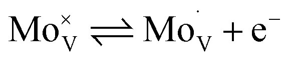
VO(acac)2 was chosen as a low-cost and widely available starting material. This blue compound, dissolves in acetone to give a blue solution, however, the colour rapidly becomes paler and more green upon addition of (wet) MeOH (Fig. 1a). This is due to the rapid reaction with MeOH and water, reported to form [VO(OH)(Ome)(acac)]−, along with release of one H(acac).69 Under air, this green solution slowly oxidises to generate diamagnetic orange V(V) species which can be studied by 51V NMR spectroscopy (50% oxidation occurs after ∼13 h, Fig. 1c). 51V NMR was conducted on a 5 mM solution of VO(acac)2 + BiPh3 in 3:1 d6-acetone/d4-MeOH, consistent with the precursor solution used for material synthesis, after ageing under air for 30 h. The spectrum (collected over 12 h) revealed three 51V signals at −492 ppm (9%), −502 ppm (30%) and −574 ppm (61%) (Fig. 1b). The major signal at −574 ppm is attributed to VO(Ome)3,70 without associated acac ligands (N.B. the 51V chemical shift of VO(Ome)3 is reported to be sensitive to concentration and solvent, due to molecular association). The minor signals are attributed to VO(Ome)(acac)2 (−492 ppm) and the dimeric [VO(Ome)2(acac)]2 (−502 ppm) in which one acac ligand has been lost per V site, based on previously reported analysis.70 These species, along with the necessarily released acac–H, exist in an equilibrium that is sensitive to solvent and concentration. Under these high-dilution conditions, with MeOH acting as a coordinating solvent, species that have a low acac content are favoured (with free acac–H observed in the associated 1H NMR spectra) (Fig. S2a†). More concentrated solutions of VO(acac)2 in other solvents, CDCl3 (72 mM), C6D6 (36 mM) or d6-acetone (36 mM), with a smaller quantity of MeOH (<10% of solution) resulted in the same three 51V signals (with minor chemical shift changes) but with different ratios. These favour acac-rich VO(Ome)(acac)2 as the major component (Fig. S2b†). Recording the spectra at different time points after mixing indicated little change in the equilibrium position, however, at short time periods it is expected that solvolysis of the second acac ligand is much slower than the first.69 The oxidation of the precursor solution under air (in a sealed cuvette) was monitored over time by visible absorption spectroscopy (Fig. 1c), 50% of the V(IV) signal has been lost after ∼13 hours, which is consistent with loss of a broad paramagnetic signal for V(IV) species in the equivalent 1H NMR data (Fig. S2c†). The oxidation of VO(acac)2 in MeOH has been reported to be first-order with respect to both [VO(acac)2(MeOH)] and O2,69 which was consistent with the conditions studied here, when followed by the loss of the d–d transition absorption signal centred around 750 nm (Fig. 1c and S2d†). The formation of oxidised species causes a change to an orange solution. The kinetics associated with the increase in absorption in the V(V) ligand to metal charge transfer region (<550 nm) are complex, indicating the formation of a shifting equilibrium of species during the transformation (Fig. S2e†). At early time points the LMCT absorptions increase linearly, e.g. with ∼0th order kinetics, the LMCT band then increases at an elevated rate between 5–7 hours before dropping to a slower rate over prolonged time periods.
 | ||
| Fig. 1 (a) Photos (left to right) of VO(acac)2 dissolved in acetone, acetone/MeOH, and then after ageing under air. (b) 51V NMR spectrum of a 5 mM solution of VO(acac)2 + BiPh3 in deuterated acetone/MeOH (3:1) after oxidation for 30 h under air. (c) Visible absorption spectra of a 5 mM solution of VO(acac)2 in acetone (bold blue line) and 5 mM solution of VO(acac)2 in acetone/MeOH (3:1) over time (bold green line, t = 0 min; bold gold line, t = 3010 min; bold orange line, t = 7200 min). BiPh3 was added at the end of the experiment but has no effect on the absorption spectrum. | ||
Whilst colourless Mo(CO)6 is poorly soluble in acetone/MeOH, slow partial dissolution to give a pale yellow solution occurs over 24 hours. Dissolution is accelerated in the presence of two equiv. acac–H, to give an orange solution. This solution shows a broad 1H NMR signal at 15.5 ppm, suggesting a paramagnetic Mo compound with organic (acac) ligands. Mo6+O2(acac)2 is a well-known compound, but would not give a paramagnetic signal, therefore a lower oxidation state of Mo is expected under these conditions. It is possible that reduced Mo compounds form in the precursor solution, especially if acac–H is released during the oxidation of V species. The exact Mo speciation is not easily probed due to the low solubility of Mo(CO)6. Acetone/MeOH solutions of BiPh3 were examined by 1H NMR spectroscopy, revealing the chemical inertness of BiPh3 under air/moisture and in the presence of VO(acac)2, oxidised V5+ species (including excess acac–H) and Mo(CO)6 when studied by 1H NMR (Fig. S2a†). It appears that BiPh3 remains a well-defined complex under these conditions.
It is clear that the precursor solution is prone to ageing effects over time, driven by the oxidation of V4+ by air in the presence of MeOH, which in turn may release acac–H which could, in turn, ligate to oxidised Mo species. Ageing effects are known in the literature in related metal–organic decomposition processes to access BiVO4.71 Herein, to minimise the effect of ageing in our work, each precursor solution was made fresh for each CVD reaction and used within a period of ∼30 min.
3.2. Physical characterisation
:BiVO4 sample), with no additional phases observed. In undoped BiVO4, the metastable tetragonal scheelite phase undergoes a phase change to the thermodynamic monoclinic clinobisvanite phase at ∼255 °C.45,72 Herein, the addition of Mo-dopants were found to prevent this phase change, despite the coatings being grown at 400 °C and subsequently annealed in air at 500 °C. This effect was previously observed by Fischer et al. in their MOD grown Mo-doped BiVO4 films, where they saw a continuous transition from the monoclinic clinobisvanite to tetragonal scheelite phase with increasing Mo-doping.37 In their case, the full transition to tetragonal scheelite was observed with ∼10.5% Mo-doping. This was also seen by Xiao et al. in their electrodeposited Mo-doped BiVO4 films, were full transition to the tetragonal scheelite phase was found with ∼10% Mo-doping.34 Herein, our XRD results indicated a full transition to the tetragonal scheelite phase with only ∼2% Mo-doping.
 | ||
| Fig. 2 (a) XRD patterns, (b) close-up view of select peaks in XRD patterns, (c) Raman spectra and (d) close-up view of select peaks in Raman patterns of BiVO4 and all Mo-doped BiVO4 samples. | ||
Le Bail models were fit to the XRD patterns, yielding the lattice parameters and average crystal sizes in our coatings. These parameters are plot in Fig. S3† and listed in Table 1. Comparing changes with Mo-doping to an undoped tetragonal scheelite standard (I41/a; a = b = 5.105(1) Å, c = 5.0821(3) Å, c = 11.577(1) Å, α = β = γ = 90°),73 we see that the a lattice parameter tended to increase as the Mo-doping level was increased; rising from 5.1903(3) Å in the undoped BiVO4 standard to 5.1349(2) Å in 12% Mo:BiVO4 (Fig. S3a†). However, the reverse trend was seen for the c lattice parameter; decreasing from 11.6705(9) Å in the undoped BiVO4 standard to 11.5592(7) Å in 12% Mo:BiVO4. Overall, there was a general trend for the unit cell volume to increase with Mo-doping; increasing from 301.7(1) Å3 in the undoped BiVO4 standard to 304.8(2) Å3 in 12% Mo:BiVO4. This trend is intuitive, as the Mo6+ dopants in a 4-coordinate environment have a higher ionic radius (r ∼0.41 Å) than the V5+ sites they replace (r ∼0.355 Å), causing the unit cell to expand to accommodate them. Correlating with this trend was the increase in average crystal size, increasing from ∼25.2 nm in 1% Mo:BiVO4 to ∼44.5 nm in 12% Mo:BiVO4.
| BiVO4 | 1% Mo–BiVO4 | 3% Mo–BiVO4 | 6% Mo–BiVO4 | 12% Mo–BiVO4 | ||
|---|---|---|---|---|---|---|
| a Light power is ∼8.5 mW cm−2. Numbers in brackets represent the standard error on the lowest significant figures. | ||||||
| XRD | Crystal type | Clinobisvanite | Scheelite | Scheelite | Scheelite | Scheelite |
| Symmetry | Monoclinic | Tetragonal | Tetragonal | Tetragonal | Tetragonal | |
| a (Å) | 5.190(3) | 5.120(5) | 5.119(5) | 5.120(3) | 5.134(2) | |
| c (Å) | 11.670(9) | 11.575(10) | 11.575(10) | 11.561(8) | 11.559(7) | |
| γ (°) | 90.3(1) | 90 | 90 | 90 | 90 | |
| unit cell (Å3) | 307.8(3) | 303.5(5) | 303.3(5) | 303.1(3) | 304.7(2) | |
| Crystal size (nm) | 32 | 25 | 25 | 36 | 45 | |
| XPS | Mo:V (%) |
— | 2.0(1) | 4.3(4) | 9.6(4) | 12.7(14) |
| AFM | R q (nm) | 22.5 | 19.7 | 17.2 | 27.2 | 20.7 |
| Surface area per square micron (μm2) | 1.10 | 1.13 | 1.04 | 1.23 | 1.08 | |
| UV-vis | E bg indirect (eV) | 2.55 | 2.56 | 2.54 | 2.54 | 2.55 |
| E bg direct (eV) | 2.62 | 2.62 | 2.61 | 2.65 | 2.65 | |
| PEC front | 400 nm (mA cm−2) | 0.21 | 0.41 | 0.45 | 0.82 | 0.60 |
| TSP (mA cm−2) | 0.48 | 0.91 | 1.02 | 1.79 | 1.38 | |
| PEC back | 400 nm (mA cm−2) | 0.23 | 0.25 | 0.31 | 0.34 | 0.23 |
| TSP (mA cm−2) | 0.55 | 0.59 | 0.74 | 0.78 | 0.59 | |
Raman spectroscopy of the undoped BiVO4 sample corroborated with XRD data, indicating the formation of the monoclinic form (Fig. 2c). The major peaks seen at ∼213, ∼328, ∼368 and ∼831 and cm−1 corresponded to the external lattice, Ag asymmetric V–O bending, Bg symmetric V–O bending and the Ag symmetric V–O stretching modes, respectively.74 However, upon doping with increasing levels of Mo, a gradual merging of the Ag asymmetric and Bg symmetric V–O bending modes was observed, whereby at 12% Mo-doping the peaks had almost completely merged (Fig. 2d). In addition, we see the introduction of a satellite peak at ∼881 cm−1, which increased in intensity with increased Mo-doping, which has previously been assigned to the introduction of a Mo–O–Mo stretching mode.75 Another effect was the general decrease in energy of all prominent peaks with increased Mo-doping, which is consistent with the elongation of V–O bond length,75,76 and therefore, an expansion of the unit cell; corroborating with XRD modelling results (Table 1).
BiVO4 showed the expected peaks in the Bi 4f, V 2p and O 1s binding energy environments. For the Bi 4f environment, Bi 4f7/2 and Bi 4f5/2 peaks were seen at ∼158.7 and ∼164.0 eV, respectively, which have previously been attributed to Bi3+ states in BiVO4.35 No metallic Bi states were observed in the undoped material. For the V 2p environment, V 2p3/2 and V 2p1/2 peaks were seen at ∼516.1 and ∼523.7 eV, respectively, which have previously been attributed to V5+ states in BiVO4.35 A small presence (<4% of the V content) of a reduced V species was observed, with V 2p3/2 and V 2p1/2 peaks seen at ∼514.7 and ∼522.3 eV, respectively, which were attributed to the presence of V4+ states.77 The O 1s environment showed two states; one at ∼529.3 eV, which was attributed to metal–oxygen bonds,78 and another at ∼533 eV, which was attributed to carbon–oxygen bonds.79 The abundance of each element was determined from the peak areas of each environment and corrected using relative sensitivity factors.80 At the sample surface – as XPS measures ∼10 nm deep81 – the undoped BiVO4 coating was found to be Bi-rich and V-poor. Measurement of the valence band energy region in undoped BiVO4 revealed a valence band maximum, with respect to the Fermi level, of ∼1.9 eV (Fig. S5†).
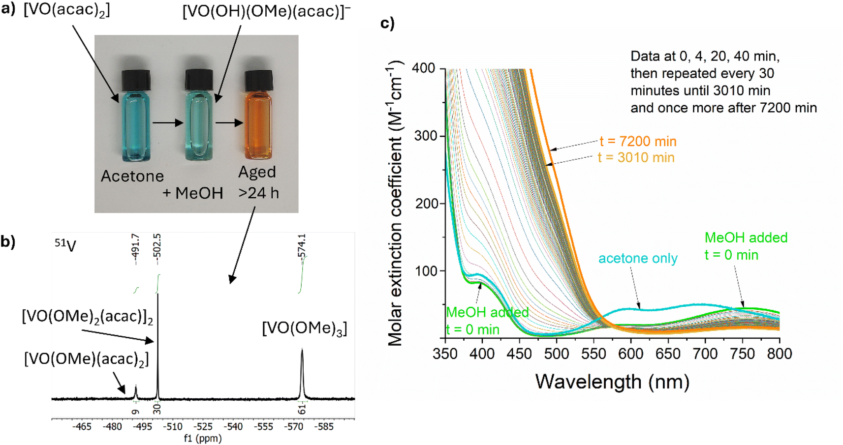
The series of Mo-doped BiVO4 showed broadly similar behaviour to undoped BiVO4, with some notable differences: (i) the binding energy of Bi3+ states tended to increase with Mo-doping and (ii) V4+ content tended to increase with Mo-doping. As expected, Mo-doped BiVO4 samples showed the presence of Mo species. Across all Mo-doped samples, the average binding energy of the Mo 3d5/2 state was ∼232.3 eV, in agreement with previous studies of Mo-doped BiVO4, and the assignment of a Mo6+ environment that substitutes V5+ sites.30–32 Relating this binding energy with previous work on molybdenum oxides, we see that this shows a closer match to Mo4O11 (Mo5.5+; 232.1 eV)82 as compared with MoO3 (Mo6+; 232.9 eV)83 and Mo2O5 (Mo5+; 231.8 eV).84 The Mo:V (%) was determined for all samples, and plot in Fig. 3. With increases in Mo precursor doping level, the amount of actual Mo-doping found in the coatings is supra-linear (i.e. Mo from the Mo precursor is more effective in entering the BiVO4 host lattice than V from the V precursor). However, at higher doping levels (from 6 to 12% Mo precursor doping level) a near linear relationship is seen, which may be due to a nearing of the solubility limit of Mo doping in BiVO4. Importantly, as the Mo-doping level was increased in BiVO4, the valence band maximum (VBM) energy did not significantly change (∼1.9 to 2.0 eV; Table S1†). This strongly indicated that Mo doping does not alter the electronic states of the VBM region in BiVO4.
 | ||
| Fig. 3 A plot of the relationship between Mo precursor dopant level (Mo:V %) vs. the Mo doping level determined by XPS analysis. All values are the average of 3 unique sample locations; with the error bars representing one standard deviation. | ||
:BiVO4) revealed densely packed irregular particles, that were predominantly between ∼100 and 150 nm wide (Fig. 4b). XRD modelling showed that average crystal sizes ranged from ∼25 to 45 nm in our coatings (Table 1). This indicated the particles seen in SEM were composed from a number of nanocrystals. The coating thickness of a representative 6% Mo:BiVO4 coating was found to be ∼180 nm by side-on SEM imaging (Fig. S6†). Top-down AFM images revealed similar topographies to top-down SEM images for both the undoped BiVO4 (Fig. 4c) and series of Mo-doped BiVO4 coatings (Fig. 4d and S7†). From AFM images, the root mean square roughness (Rq) and surface area per square micron were determined for all samples (Table 1). The Rq ranged from ∼17.2 to ∼27.2 nm and the surface area per square micron ranged from 1.04 to 1.23 μm2. No observable trend between the level of Mo-doping and surface roughness or surface area was found. Broadly speaking, all coatings were highly smooth, and showed minimal differences in surface area (up to ∼15%).
 | ||
| Fig. 4 SEM images of (a) BiVO4 and (b) 6% Mo–BiVO4 taken at 50k magnification [the width of each image represents a distance of 3.8 μm]. AFM images, of (c) BiVO4 and (d) 6% Mo–BiVO4 measured over a 1 μm × 1 μm square area. | ||
 | ||
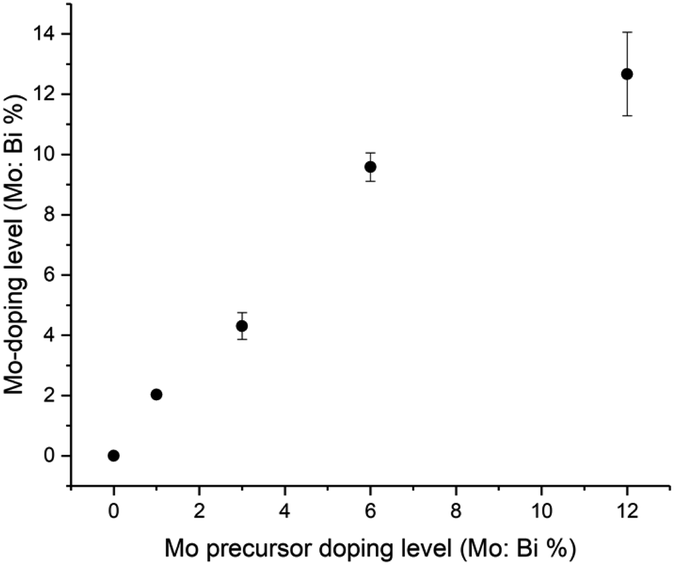
| Fig. 5 (a) UV-visible absorption spectra of BiVO4 and all Mo-doped BiVO4 samples and light remaining (%) with distance travelled in 6% Mo–BiVO4 for (b) front irradiation and (c) back irradiation (shaded green and grey areas represent BiVO4 [180 nm thick] and FTO [320 nm thick] layers respectively). | ||
With knowledge of the coating thickness (Fig. S6†), the UV-visible absorption data was used to determine the penetration depth of light (Fig. S8b†).87 This was used to calculate how different wavelengths of light are absorbed as they travel through our materials, and was done for the cases of UVA (325 nm), violet (400 nm) and blue (475 nm) light for the scenarios of front (Fig. 5b) and back (Fig. 5b) irradiation. Under front irradiation, most UVA (∼99%) and violet (∼85%) light is absorbed within 100 nm of entering the photoanode. However, only ∼43% of blue light is absorbed within 100 nm of entering the photoanode, and only ∼64% of blue light is absorbed across the entire 180 nm coating. Under back irradiation, light travels through the FTO layer before reaching the photoanode. Substantial parasitic light absorption is seen in the FTO layer, with this being most significant in the UVA region (∼60% absorbed across the 320 nm FTO coating). The remaining UVA is mostly absorbed (∼39%) within the first 100 nm of entering the photoanode. For the cases of violet and blue light, only ∼20% of light is parasitically absorbed by the FTO layer. Within 100 nm of entering the photoanode, ∼68% and ∼35% of the remaining violet and blue light is absorbed, respectively. Under back irradiation, across the entire photoanode, ∼39%, ∼78% and ∼52% of UVA, violet and blue light is absorbed, respectively. Whereas under front irradiation, ∼100%, ∼97% and ∼64% of UVA, violet and blue light is absorbed, respectively.
3.3. Photoelectrochemical water splitting
The PEC water oxidation performance of our undoped BiVO4 and series of Mo-doped BiVO4 was investigated using current–voltage (JV) curves in 0.1 M phosphate buffer under 400 nm excitation (Fig. 6). All samples showed similar dark electrocatalytic behaviour, with the onset for water oxidation seen at ∼2.0 VRHE. Under illumination, all samples showed a similar onset to photocatalytic water oxidation at ∼0.6 VRHE, and did not change for front or back irradiation.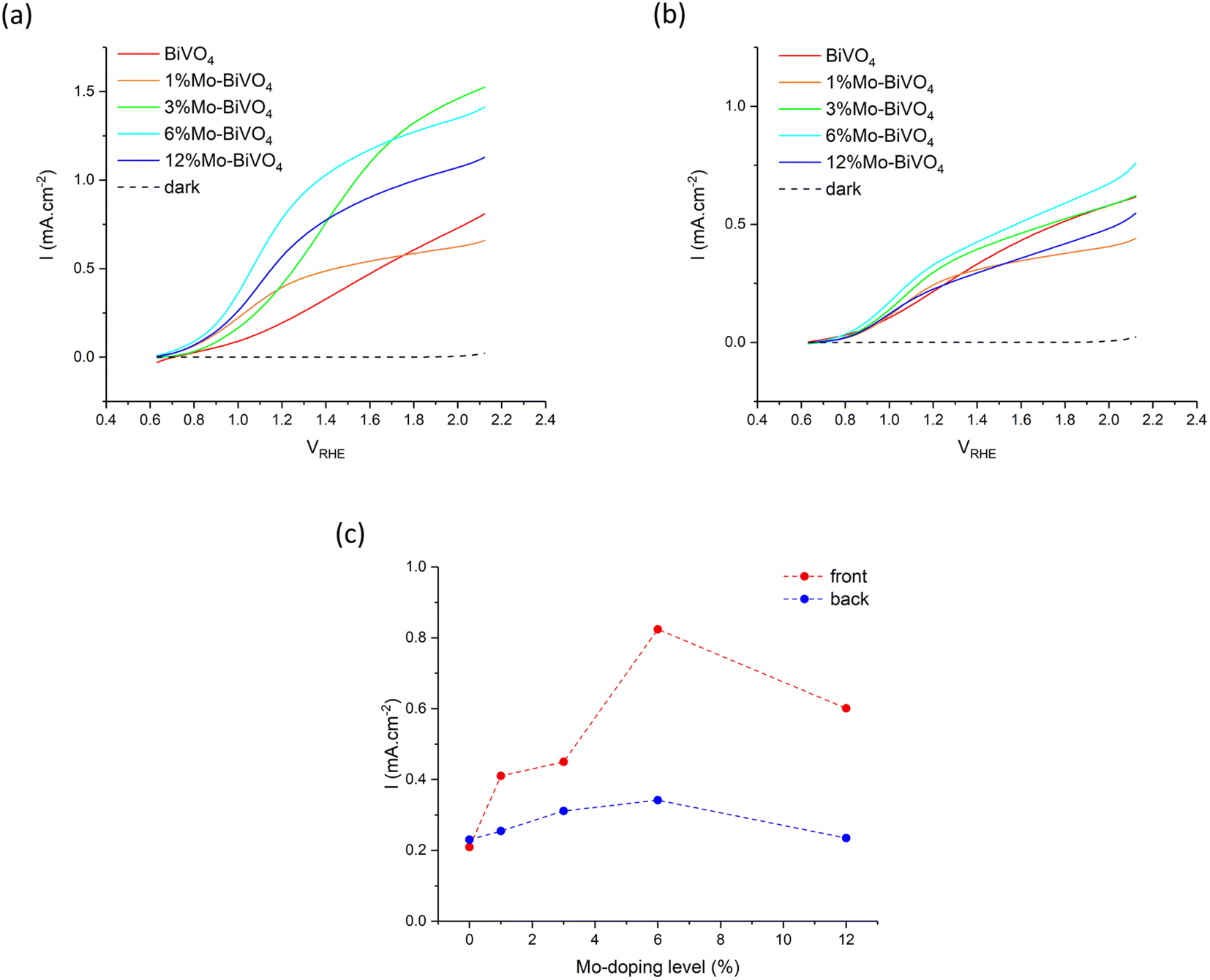 | ||
| Fig. 6 Current voltage (JV) curves for BiVO4 and all Mo-doped BiVO4 samples measured with (a) front irradiation and (b) back irradiation. (c) The photocurrent densities observed at 1.23 VRHE for both front and back irradiation as a function of Mo precursor doping level (%) of BiVO4 and all Mo-doped BiVO4 samples. Samples were measured in 0.1 M phosphate buffer (pH = 7) using 400 nm light (∼8.5 mW cm−2). | ||
Under front irradiation, the undoped BiVO4 sample showed a slower rise in photocurrent density than the Mo-doped BiVO4 samples, which was indicative of a higher barrier to electron carrier extraction in BiVO4 (Fig. 6a). Although the highest plateau photocurrent density is seen in the 3% Mo:BiVO4 sample, reaching ∼1.5 mA cm−2 at 2.1 VRHE, the 6% Mo:BiVO4 sample showed the highest photocurrent density at 1.23 VRHE of ∼0.82 mA cm−2.
Under back irradiation, all samples showed similar PEC behaviour (Fig. 6b). There was a notable faster rise in photocurrent density in the undoped BiVO4 sample than was seen under front irradiation, which was indicative of a comparatively lower barrier to hole carrier diffusion than electron carrier extraction in the material. Under back irradiation, the 6% Mo:BiVO4 sample showed the highest plateau photocurrent density, reaching ∼0.75 mA cm−2 at 2.1 VRHE, and highest photocurrent density at 1.23 VRHE of ∼0.34 mA cm−2.
Comparing front and back irradiation, the Mo-doped BiVO4 samples showed notably higher photocurrent densities under front irradiation than back irradiation. A plot of the photocurrent density at 1.23 VRHE for front and back irradiation for all samples is shown in Fig. 6c. Similar trends were observed for front and back irradiation, with the photocurrent density consistently rising with increases in Mo precursor doping to 6% Mo:V, before falling at 12% Mo:V. With the exception of the undoped BiVO4 sample, the photocurrent density at 1.23 VRHE was consistently higher for front irradiation than back irradiation. The 6% Mo:BiVO4 sample showed the highest performance in both cases, reaching photocurrent densities of ∼0.82 and ∼0.34 mA cm−2 for front and back irradiation, respectively. Comparing the photocurrent densities seen at 1.23 VRHE, the performance under front irradiation was up to 2.6 times better than under back irradiation (Table 1). These differences could not be rationalised from the subtle differences in light harvesting of the 400 nm light source, with ∼97% absorbed under front irradiation and ∼78% absorbed under back irradiation (Fig. 5). Rather, the increases in front irradiation performance, found with Mo-doping, were attributed to enhancements in electron carrier transport and extraction. As back irradiation performance was broadly the same across the series of samples, we conclude that this effect was predominantly limited to improving electron transport (i.e. hole carrier transport was largely unaffected by Mo-doping).
The incident photon-to-current efficiency (IPCE) was measured at 1.23 VRHE in 0.1 M phosphate buffer under front and back irradiation for all samples (Fig. 7). Under front irradiation, the undoped BiVO4 sample showed IPCEs of up to ∼10% in the ultra-bandgap region. The 6% Mo:BiVO4 sample showed the highest IPCEs, reaching ∼50% at 325 nm. Similar to JV curve measurements, the IPCE performance consistently increased with Mo-doping from 0 to 6% Mo:V, and then decreased at 12% Mo:V. Under back irradiation, IPCEs were significantly lower than those measured under front irradiation. This, in part, was due to the parasitic absorption of light by the FTO substrate, which absorbed most strongly in the UV region. However, IPCEs in the visible region where the parasitic absorption of light was limited (to ∼20%) were substantially lower than those measured under front irradiation. Under back irradiation, the 6% Mo:BiVO4 sample showed the highest IPCEs, reaching ∼14% at 400 nm. This was less than half the value observed under front irradiation (∼30% at 400 nm). Importantly, under back irradiation, Mo-doping granted only marginal increases in performance compared with undoped BiVO4, which is in line with the accepted hypothesis that Mo-doping primarily improves the conductivity of photo-generated electron carriers.
 | ||
| Fig. 7 Incident photon to current efficiency (IPCE) curves for BiVO4 and all Mo-doped BiVO4 samples measured with (a) front irradiation and (b) back irradiation. Samples were measured in 0.1 M phosphate buffer (pH = 7) at 1.23 VRHE. | ||
Under front irradiation, the highest IPCEs were seen in the UV region, where light is absorbed most prominently near the surface of the material (∼75% of 325 nm light absorbed within 30 nm of entering the material). Under front irradiation, the 6% Mo:BiVO4 sample showed IPCEs in the ultra-bandgap region between 4 and 5 times higher than undoped BiVO4, whereas under back irradiation, the 6% Mo:BiVO4 sample showed IPCEs in the ultra-bandgap region between 1 and 1.5 times higher than undoped BiVO4. As the optical properties of both materials were similar, overall, these trends indicated that electron carrier transport and extraction was enhanced by a factor of between 4 and 5 with Mo doping, and that hole carrier transport was largely unaffected.
The theoretical solar photocurrent (TSP) was determined by multiplying the IPCE measured at 1.23 VRHE with the solar spectrum (AM1.5) and integrating the photon-to-current flux (eqn (4); Fig. 8). Undoped BiVO4 showed TSPs of ∼0.48 and ∼0.55 mA cm−2 for front and back irradiation, respectively. In all cases, Mo-doping increased the TSP, with 6% Mo:BiVO4 showing the highest TSPs of ∼1.79 and ∼0.78 mA cm−2 for front and back irradiation, respectively. Similar to JV and IPCE curves, TSPs were significantly higher (up to a factor of ∼2.3) for front irradiation than back irradiation. This, as mentioned above, is attributed to the improvement in electron carrier transport and extraction with Mo-doping.
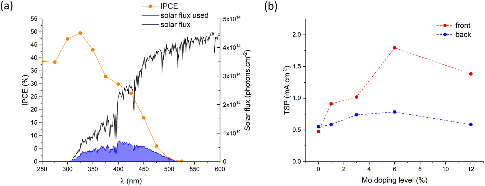 | ||
| Fig. 8 (a) Calculation of the theoretical solar photocurrent (TSP) for 6% Mo–BiVO4 under front irradiation at 1.23 VRHE and (b) a summary of the TSP photocurrents at 1.23 VRHE for front and back irradiation as a function of Mo precursor doping level (%) of BiVO4 and all Mo-doped BiVO4 samples. | ||
The photoelectrochemical water oxidation performance of the samples produced herein is now compared with the literature; summarised in Table 2. Herein, we compare BiVO4 produced by CVD routes (akin to this work) and Mo-doped BiVO4 produced by any synthetic route. It should be noted, for fair comparisons to be made, more complex BiVO4-based structures are not included in this table (e.g. surface modified BiVO4 with a co-catalyst to improve surface reaction kinetics, or the formation of a BiVO4-based heterojunction to improve charge carrier separation, etc.).
| Photoanode | Synthesis method |
Mo:V doping level (%) |
Material structure | J on (VRHE) | J (mA cm−2) | Reference |
|---|---|---|---|---|---|---|
| a Represents the amount added during synthesis, and in brackets, represents the amount measured by an analytical technique. b The photocurrent onset potential. c Photocurrent observed at 1.23 VRHE using a simulated solar light source of 1 sun power (100 mW cm−2) or TSP derived from IPCE measurements. na = not applicable; ns = not stated. d Examined in a hole scavenger solution. e Lamp power not stated. f Measured at ∼1.13 VRHE. | ||||||
| BiVO4 | AA-CVD | na | Porous irregular particles (∼500 nm wide) | ∼1.0 | ∼0.15 | Sagu et al.15 |
| na | Porous irregular particles (∼75 nm wide) | ∼0.6 | ∼0.40 | Sagu et al.14 | ||
| DLI-CVD | na | Densely packed rounded particles (∼0.2 to 1 μm wide) | ∼0.23 | ∼2.10 | Gupta et al.17 | |
| VT-CVD | na | Densely packed rounded particles (∼200 nm) | ∼0.3d | ∼0.95d | Ager et al.16 | |
| AA-CVD | na | Densely packed cuboidal particles (∼200 nm wide) | ∼0.6 | ∼0.55 | herein | |
| Mo–BiVO4 | Electro-deposition | 1.25 (1.8) | Open nanoporous structure | ∼0.5 | ∼0.85 | Choi et al.88 |
| ns (ns) | Wormlike nanostructure (∼100 nm wide) | ∼0.4 | ∼1.4 | Ao et al.35 | ||
| 3 (3) | Wormlike nanostructure (∼100 nm wide) | ∼0.55 | ∼1.9 | Xiao et al.34 | ||
| Electro-spinning | ns (ns) | 1D nanofibres | ∼0.7 | ∼0.15 | Hwang et al.31 | |
| 2.0 (3.0) | Irregular mesoporous network | ∼0.5 | ∼0.77 | Wong et al.30 | ||
| ESD | 0.15 (ns) | Nanotextured pillars (∼10 μm tall) | ∼0.7 | ∼0.7 | Yoon et al.32 | |
| MOD | 2.0 (4.5) | Mesoporous structure | ∼0.4 | ∼0.4 | Herring et al.41 | |
| 0.5 (ns) | Dense, irregularly particles (∼50 nm wide) | ns | ∼1.1d,f | Kudo et al.38 | ||
| 10 (6) | Dense, wormlike particles (∼50 nm wide) | ∼0.5 | ∼1.9 | Fischer et al.37 | ||
| ns (3.0) | Nanoporous (∼100 nm wide particles) | ∼0.4 | ∼2.1 | Cui et al.39 | ||
| 3.0 (6.5) | Compact nanoporous structure (∼150 nm wide particles) | ∼0.4 | ∼2.2e | Zou et al.40 | ||
| PVD | 1.0 (1.0) | Nanostructured wormlike arrays (∼100 nm in diameter) | ∼0.3d | ∼2.1d | Zhang et al.43 | |
| ns (3.0) | Porous irregular particles (∼200–400 nm wide) | ∼0.3d | ∼3.5d | Ager et al.42 | ||
| AA-CVD | 6.0 (9.6) | Densely packed irregular particles (∼100 to 150 nm wide) | ∼0.6 | ∼1.79 | herein | |
Sagu et al. used an AA-CVD method to produce m-BiVO4 photoanodes.14,15 Porous irregular particles (∼500 nm wide) of BiVO4 were formed when ethylene glycol was used to dissolve their bismuth precursor, which when examined in 0.5 M Na2SO4(aq.), showed an onset potential of ∼1.0 VRHE and a photocurrent density of ∼0.15 mA cm−2 at 1.23 VRHE and 1 sun irradiance.15 Smaller porous irregular particles (∼75 nm wide) of BiVO4 were formed when acetylacetone was used to dissolve their bismuth precursor, which when examined in 1 M Na2SO4(aq.), showed an onset potential of ∼0.6 VRHE and a photocurrent density of ∼0.40 mA cm−2 at 1.23 VRHE and 1 sun irradiance.14 Gupta et al. used a DLI-CVD method to produce m-BiVO4 photoanodes.17 Densely packed rounded particles (∼0.2 to 1 μm wide) of BiVO4 were formed, which when examined in 0.5 M KOH(aq.), showed an onset potential of ∼0.23 VRHE and a photocurrent density of ∼2.10 mA cm−2 at 1.23 VRHE and 1 sun irradiance (although it should be noted that the photocurrent density decreased rapidly in this high pH electrolyte). Ager et al. used a VT-CVD method to produce m-BiVO4 photoanodes.16 Densely packed rounded particles (∼200 nm) of BiVO4 were formed, which when examined in a hole scavenger solution of 0.5 M Na2SO3(aq.), showed an onset potential of ∼0.3 VRHE and a photocurrent density of ∼0.95 mA cm−2 at 1.23 VRHE and 1 sun irradiance. Herein, an AA-CVD method was used to produce m-BiVO4 photoanodes. Films with densely packed cuboidal particles (∼200 nm wide) of BiVO4 were formed, which when examined in 0.1 M phosphate buffer, showed an onset potential of ∼0.6 VRHE and a TSP of ∼0.55 mA cm−2 when irradiated from the back. The PEC performance of the BiVO4 photoanodes grown herein, using AA-CVD, compared favourably with previous work where alternative CVD routes were also used; displaying median onset potentials and photocurrent densities (Table 2).
Mo-doped BiVO4 has been synthesised using a range of methods.30–32,34–43 Choi et al. used an electrodeposition method to produce Mo-doped BiVO4 with open nanoporous structures.88 They studied range of precursor doping levels from 0.5 to 3%, and found that the most photoelectrochemically active sample contained 1.8% Mo:V. They studied the activity of this sample in 1 M NaH2PO4 buffer, which showed an onset potential of ∼0.5 VRHE and a photocurrent density of ∼0.85 mA cm−2 at 1.23 VRHE and 1 sun irradiance. Ao et al. also used an electrodeposition method to produce Mo-doped BiVO4.35 The films possessed worm-like nanostructure (∼100 nm wide). Their samples were tested in 0.1 M Na2SO4(aq.), with the most active sample showing an onset potential of ∼0.4 VRHE and a photocurrent density of ∼1.4 mA cm−2 at 1.23 VRHE and 1 sun irradiance. To our knowledge, the Mo-doping level was not stated for these samples (despite XPS analysis being carried out). And Xiao et al. produced Mo-doped BiVO4 by electrodeposition.34 Similar to Ao et al.,35 worm-like nanostructures were formed. A range of doping concentrations were examined (from ∼1 to ∼10%), with the most active sample containing ∼3% Mo:V. In 0.5 M phosphate buffer, the best performing sample showed an onset potential of ∼0.55 VRHE and a photocurrent density of ∼1.9 mA cm−2 at 1.23 VRHE and 1 sun irradiance.
Hwang et al. grew Mo-doped BiVO4 using an electrospinning method, producing 1D nanofibers.31 The best performing sample, when examined in 0.1 M phosphate buffer, showed an onset potential of ∼0.7 VRHE and a photocurrent density of ∼0.15 mA cm−2 at 1.23 VRHE and 1 sun irradiance. The Mo-doping level added or achieved was not stated. Wong et al. also used electrospinning route, producing Mo-doped BiVO4 films formed from irregular mesoporous networks.30 Their best performing sample contained 3% Mo:V, and when examined in 0.5 M Na2SO4(aq.), showed an onset potential of ∼0.5 VRHE and a photocurrent density of ∼0.77 mA cm−2 at 1.23 VRHE and 1 sun irradiance.
Yoon et al. grew Mo-doped BiVO4 using an ESD method, forming nanotextured pillars that were ∼10 μm tall.32 They studied a range of Mo-doping levels from 0.05 to 0.20%, and found that the highest performance was seen in films with a 0.15% precursor doping level. The photoelectrochemical activity was investigated in 1 M Na2SO4, showing an onset potential of ∼0.7 VRHE and a photocurrent density of ∼0.7 mA cm−2 at 1.23 VRHE and 1 sun irradiance.
Using a surfactant-assisted MOD route, Herring et al. produced mesoporous Mo-doped BiVO4 films.41 Their optimal sample was produced from a 2.0% Mo:V precursor ratio, producing a film with 4.5% Mo:V doping. This was examined in 0.5 M Na2SO4(aq.) phosphate buffer, and showed an onset potential of ∼0.4 VRHE and a photocurrent density of ∼0.4 mA cm−2 at 1.23 VRHE and 1 sun irradiance. Kudo et al. produced densely packed, irregularly shaped particles (∼50 nm wide) using MOD.38 A range of Mo precursor doping levels were studied (from 0.25 to 1.5%). The optimum Mo precursor doping level was found to be 0.5%; however, the doping level achieved in the sample was not stated. The photoanode was studied in 0.1 M K2SO4(aq.) in the presence of a hole scavenger 0.01 M K2SO3(aq.), and achieved a photocurrent density of ∼1.1 mA cm−2 at ∼1.13 VRHE at 1 sun irradiance. Fischer et al. also used MOD to synthesise Mo-doped BiVO4.37 Their coatings were made of dense, wormlike particles (∼50 nm wide). A wide range of Mo precursor doping levels were studied (0 to 20%). The sample containing 6% Mo:Bi doping showed the highest photoelectrochemical performance, where when examined in 0.1 M potassium phosphate buffer, showed an onset potential of ∼0.5 VRHE and a photocurrent density of ∼1.9 mA cm−2 at 1.23 VRHE and 1 sun irradiance. Nanoporous (∼100 nm wide particles) Mo-doped BiVO4 was produced using MOD by Cui et al.39 Their best performing sample contained a 3% Mo:V doping level, and when examined in 0.5 M KH2PO4 buffer, showed an onset potential of ∼0.4 VRHE and a photocurrent density of ∼2.1 mA cm−2 at 1.23 VRHE and 1 sun irradiance. And Zou et al. used MOD to synthesise compact nanoporous films of Mo-doped BiVO4.40 Their most active sample was contained 6.5% Mo:V, which when examined in 0.5 M Na2SO4(aq.), showed an onset potential of ∼0.4 VRHE and a photocurrent density of ∼2.2 mA cm−2 at 1.23 VRHE (Xe lamp; irradiance power not stated).
Zhang et al. grew Mo-doped BiVO4 using a pulsed laser PVD route.43 Nanostructured wormlike structures were formed, which were ∼100 nm in diameter. A range of Mo-doping levels were studied (from 0.5 to 5.0%), where it was found that 1.0% Mo:V doping resulted in the highest performing photoanodes. When examined in a 0.1 M phosphate buffer solution with a 0.1 M Na2SO3(aq.) hole scavenger, the optimal sample showed an onset potential of ∼0.3 VRHE and a photocurrent density of ∼2.1 mA cm−2 at 1.23 VRHE and 1 sun irradiance. Ager et al. grew Mo-doped BiVO4 using a reactive co-sputtering PVD method, forming porous irregular particles (∼200–400 nm wide).42 A range of Mo-doping levels were studied (from 1.0 to 5.5%). It was found that 3% Mo:V doping resulted in the highest performing films. The photoelectrochemical performance was examined in 1 M phosphate buffer with 0.1 M Na2SO3(aq.) hole scavenger, showing an onset potential of ∼0.3 VRHE and a photocurrent density of ∼3.5 mA cm−2 at 1.23 VRHE and 1 sun irradiance.
Herein, an AA-CVD method was used to produce Mo-doped t-BiVO4 photoanodes, forming densely packed irregular particles (∼100 to 150 nm wide). A range of Mo-doping levels were investigated (from ∼2.0 to ∼12.7% doping level achieved), where the highest performance was observed (for both front and back irradiation) was a 9.6% Mo-doped sample. This sample, when examined in 0.1 M phosphate buffer, showed an onset potential of ∼0.6 VRHE and a TSP of ∼1.79 mA cm−2 when irradiated from the front. Despite there being a wide range of Mo-doping levels studied to date, there is no consensus on what the optimum Mo-doping level; ranging from ∼1.0 to 9.6% Mo:V%. This we attribute to the range of methods used to produce Mo-doped BiVO4, resulting in a wide range of topographies, average crystal sizes and defect densities. However, what can be said is that the photoelectrochemical performance of the best performing Mo-doped BiVO4 photoanode produced herein using AA-CVD showed photocurrent densities (TSP up to 1.79 mA cm−2) at the higher end of what has previously been achieved for this material (up to 2.1 mA cm−2 at 1.23 VRHE and 1 sun irradiance42) (Table 2).
3.4. Computational studies
Hybrid exchange DFT calculations studies were carried out on the BiVO4 system to determine the effect of Mo doping substituting for Bi or V sites, at 6.25 or 12.5 at%, with respect to the metal being replaced, in both the m-BiVO4 and t-BiVO4 host structures. Herein we describe the effect of Mo doping on the thermodynamically most stable structure computed and report computed PDOS and the spin density.| Mo-doped t-BiVO4 | |||||
|---|---|---|---|---|---|
| Dopant site | n/a | V | Bi | ||
| Doping level (at%) | 0 | 6.25 | 12.5 | 6.25 | 12.5 |
| a (Å) | 5.1195 | 5.1442 | 5.1522 | 5.1091 | 5.0919 |
| b (Å) | 5.1195 | 5.1307 | 5.1522 | 5.1093 | 5.0916 |
| c (Å) | 11.6278 | 11.6387 | 11.6785 | 11.6409 | 11.6409 |
| α (°) | 90 | 90 | 90 | 89.5445 | 90.1624 |
| β (°) | 90 | 90 | 90 | 90.0542 | 90.6944 |
| γ (°) | 90 | 90.7870 | 90 | 89.6033 | 90.2061 |
| Vol. (Å3) | 304.756 | 307.154 | 310.011 | 303.858 | 301.771 |
| Vol. change vs. undoped (%) | n/a | 0.79 | 1.72 | −0.29 | −0.98 |
| Mo-doped m-BiVO4 | |||||
|---|---|---|---|---|---|
| Dopant site | n/a | V | Bi | ||
| Doping level (at%) | 0 | 6.25 | 12.5 | 6.25 | 12.5 |
| a (Å) | 5.1217 | 5.1299 | 5.1293 | 5.1090 | 5.0929 |
| b (Å) | 5.1249 | 5.1447 | 5.1749 | 5.1093 | 5.0929 |
| c (Å) | 11.6549 | 11.6360 | 11.6208 | 11.6407 | 11.6419 |
| α (°) | 89.9985 | 90.0004 | 90.0032 | 90.4560 | 90.7593 |
| β (°) | 89.9989 | 89.9930 | 90.0022 | 90.0549 | 90.1496 |
| γ (°) | 90.6845 | 90.7784 | 91.1004 | 90.3914 | 90.2804 |
| Vol. (Å3) | 305.899 | 307.070 | 308.402 | 303.848 | 301.928 |
| Vol. change vs. undoped (%) | n/a | 0.38 | 0.82 | −0.67 | −1.30 |
Experimental studies conducted herein showed that our 6% Mo–BiVO4 sample produced the most active photoanode for water splitting under both front and back irradiation (Fig. 8b), which XPS, XRD and Raman spectroscopy analysis showed contained a Mo doping level of ∼9.6 at% in V sites in a t-BiVO4 structure. The calculated analogous t-BiVO4 structure, at a similar level of Mo doping (6.25 at% in V sites) is shown in Fig. 9. A comparison of the unit cell lattice parameters shows that Mo doping in V sites results in an expansion in the unit cell volume of ∼0.79% compared to the undoped structure, with the biggest change in lattice parameter seen in the a direction (∼0.48% increase). A similar level of unit cell expansion of ∼0.46% was seen experimentally in the 6% Mo–BiVO4 sample (Table 1). Our calculations showed that a higher level of Mo doping of 12.5 at% in V sites resulted in a further increase in the unit cell expansion of ∼1.72% compared to the undoped structure.
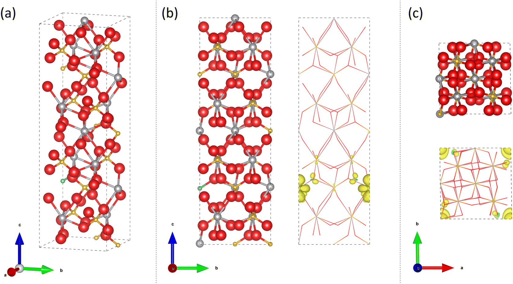 | ||
| Fig. 9 Calculated structure for 6.25 at% Mo doping of a V site in t-BiVO4 for a 2 × 1 × 1 supercell showing atomic positions and spin density [Bi = silver, V = gold, O = red, Mo = light blue; ionic radii proportions scaled down for visibility]. (a) Angled view, (b) a-axis view and (c) c-axis view. | ||
In both t-BiVO4 and m-BiVO4, V5+ ions are coordinated by four O atoms in tetrahedral sites and Bi5+ ions are coordinated by eight oxygen atoms in cubic hole sites. Comparing the Shannon crystal radii for Mo replacing such sites, one would expect an expansion in the unit cell with Mo replacing V sites and a contraction with Mo replacing Bi sites.89 In the undoped t-BiVO4 structure, the average calculated V–O bond distance in the VO4 tetrahedral units is 1.734 Å. Where the Mo dopant replaced V, the resulting MoO4 tetrahedral unit formed had an average Mo–O bond distance of 1.839 Å. This indicated that doped Mo ions have an effective radius of ∼0.11 Å larger than vanadium; this corresponds well with the Shannon ionic radii, where V and Mo ions in the 5+ state in a 4-coordinate environment show crystal radii of 0.495 Å and 0.60 Å, respectively.89
As detailed above, Mo dopants at V sites retain a single electron in a 4d derived orbital, which acts as a n-dopant and is likely to contribute to increased conductivity. The computed spin density at a Mo doping of 6.25 at% at a V site in t-BiVO4 is shown in Fig. 11b. It is clear that at this level of doping, the electron remains mostly localised to the local 4d orbital of Mo, with only some donation seen with neighbouring O ions in the MoO4 unit, and a small donation seen to nearby V ions.
The calculated structures for m-BiVO4 with 6.25 at% Mo doping of a V site is shown in Fig. S10,† t-BiVO4 and m-BiVO4 with 6.25 at% Mo doping of a Bi site are shown in Fig. S11 and S12,† respectively, t-BiVO4 and m-BiVO4 with 12.5 at% Mo doping of a V site are shown in Fig. 10 and S13,† respectively, and t-BiVO4 and m-BiVO4 with 12.5 at% Mo doping of a Bi site are shown in Fig. S14 and S15,† respectively. The lattice parameters for these Mo doped t-BiVO4 and m-BiVO4 structures are shown in Tables 3 and 4, respectively.
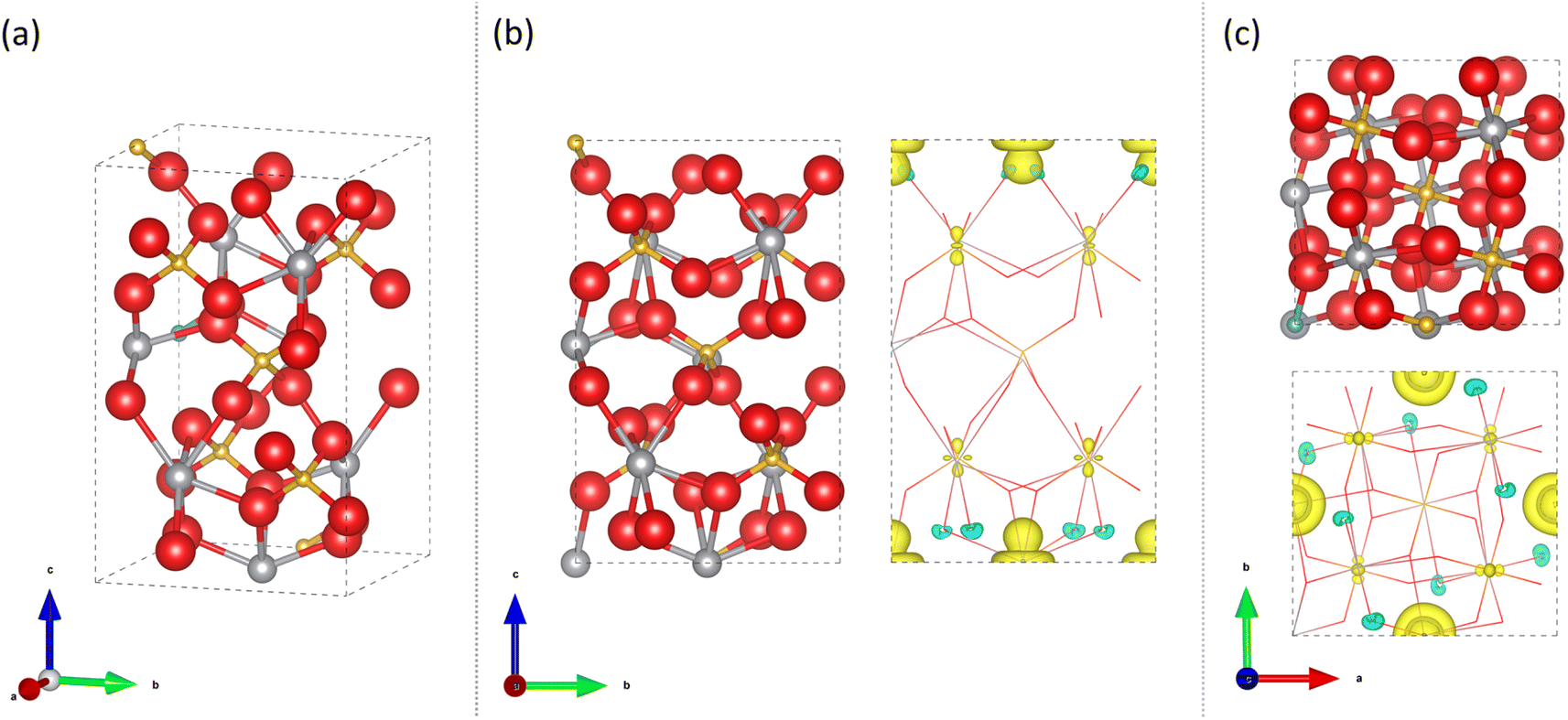 | ||
| Fig. 10 Calculated structure for 12.5 at% Mo doping of a V site in tetragonal scheelite BiVO4 for a single unit cell showing atomic positions and spin density [Bi = silver, V = gold, O = red, Mo = light blue; ionic radii proportions scaled down for visibility]. (a) Angled view, (b) a-axis view and (c) c-axis view. | ||
As expected from the localised nature of the doped electron and the effect of ionic radius on the local tetrahedral environment the overall effect on the lattice is homogeneous in the level of doping. Relatively consistent changes in the unit cell lattice parameters were seen with Mo doping in V and Bi sites for the t-BiVO4 and m-BiVO4 host structures, with expansions/contractions in volume seen with Mo doping of V/Bi sites (Fig. S16a†). This was also consistent with what was seen in our experiments, where Mo doping of V sites in a t-BiVO4 structure resulted in an expansion of the unit cell volume (Fig. S16b†), and therefore, validated our calculations. Regarding average metal oxygen bond lengths in both m-BiVO4 and t-BiVO4 structures, for the case of Mo dopants replacing V sites (i.e. tetrahedral hole sites with 4-coordinating O ions), the average bond length increased by ∼0.1 Å, and for the case of Mo dopants replacing Bi sites (i.e. cubic hole sites with 8-coordinating O ions), the average bond length decreased by ∼0.35 Å, which are both in agreement with the expected outcomes from Shannon crystal radii.89
The total energy of each calculated structure was compared (values are per unit of the largest doped supercell – 16 formula units). In line with our experiments, it was energetically more favourable, by ∼2.37 meV per cell, for undoped m-BiVO4 to form compared with undoped t-BiVO4. Again, in line with our experiments, this changed with Mo doping at 6.25 at% in V sites, with t-BiVO4 becoming more favourable by ∼2.33 meV per cell. At 12.5 at% Mo doping in V sites, the difference was negligible, with m-BiVO4 being more favourable by only ∼0.13 meV. Regarding Mo doping Bi sites, the difference was negligible at 6.25 at% doping, with t-BiVO4 being more favourable by only ∼0.19 meV, and more significant at 12.5 at% doping, with m-BiVO4 being more favourable by ∼3.05 meV. These are relatively small energetic differences and thermal fluctuations at room temperature would be expected to produce a somewhat disordered distribution of dopants amongst the available sites.
Assessing our spin density calculations, we will first discuss the effect of Mo doping in V sites. At 6.25 at% doping, the effect is similar in both t-BiVO4 (Fig. 9) and m-BiVO4 (Fig. S10†), with the 4d1 electron of Mo localising primarily on the Mo dopant site, within a single d-orbital with a distinct distribution of charge. At 12.5 at% doping in m-BiVO4, the situation is similar, with the 4d1 electron remaining quite localised to Mo (Fig. S13†). However, at 12.5 at% doping in t-BiVO4, a significant change is seen, with the 4d1 electron being completely transferred from Mo to V 3d orbitals that lie in the [001] Miller plane (Fig. 10). The exact concentration at which the delocalisation occurs will be sensitive to the treatment of electronic self-interaction and to the particular distribution of dopants in the structure. Nevertheless, it is not unreasonable to conclude that as the dopant concentration approaches 12.5 at% there is a transition from a strongly correlated insulating state to a delocalised semiconductor. This inference is further supported by our XRD data (Fig. 2), in which the peak at ∼31° 2Θ, which corresponds to diffraction in the [004] plane, increases in intensity with Mo doping, and is significantly more pronounced in the 6% Mo–BiVO4 sample. This is likely to be a result of the increased electron density in the [001] plane with Mo doping, as X-ray diffraction correlates with electron density.
Regarding the effect of Mo doping in Bi sites, at both 6.25 and 12.5 at% doping in both t-BiVO4 and m-BiVO4, the 4d3 electrons of Mo remain localised to Mo dopant sites, filling several d-orbitals to achieve a near even distribution of charge around the ion, with some spill-over seen onto neighbouring O and nearby V sites. With increased levels of Mo doping, the spillover onto neighbouring O and nearby V sites increases, however, we do not observe a transition to a delocalised state and charge remains primarily localised to Mo dopant sites.
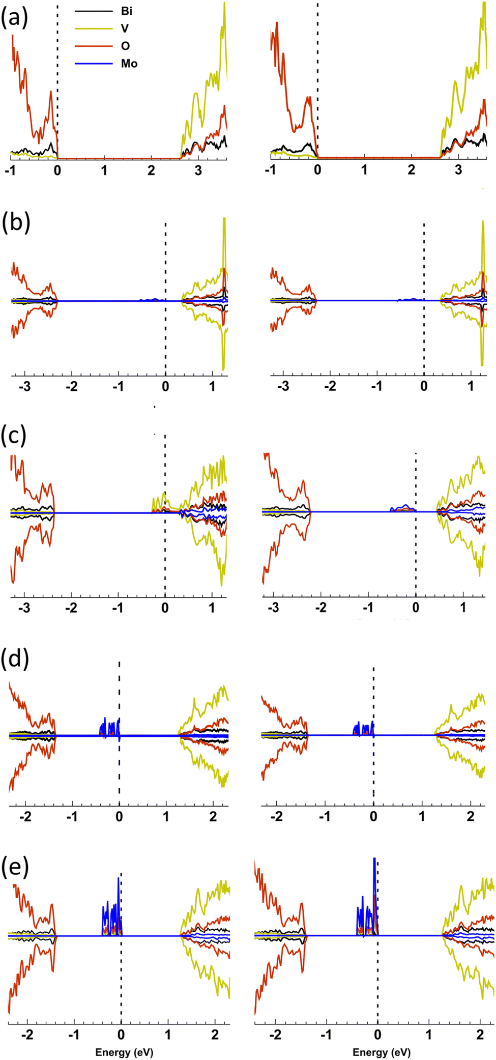 | ||
| Fig. 11 Comparison of the PDOS for (left) t-BiVO4 and (right) m-BiVO4 host structures for (a) undoped, (b) 6.25 at% Mo in a V site, (c) 12.5 at% Mo in a V site, (d) 6.25 at% Mo in a Bi site, and (e) 12.5 at% Mo in a Bi site. For each host structure, the VBM, formed primarily by O orbitals, are plot at the same position to one another. The PDOS are drawn for energies ∼1 eV below the VBM up to ∼1 eV above the CBM, which is formed primarily by V orbitals. The dashed line represents the highest occupied state in each structure. | ||
| Structure | Dopant site | Doping level (at%) | Energy gaps (eV) | ||
|---|---|---|---|---|---|
| VBM to HOS | HOS to CBM | VBM to CBM | |||
| a The HOS resides above the CBM. b Degenerate semiconductor; transition from VBM to HOS residing above the CBM. | |||||
| t-BiVO4 | n/a | 0 | 0 | 2.6639 | 2.6639 |
| V | 6.25 | ∼2.27 | 0.3483 | 2.6717 | |
| 12.5 | ∼2.28 | No gapa | 2.1451b | ||
| Bi | 6.25 | ∼1.27 | 1.244 | 2.6609 | |
| 12.5 | ∼1.28 | 1.2523 | 2.6873 | ||
| m-BiVO4 | n/a | 0 | 0 | 2.6943 | 2.6943 |
| V | 6.25 | ∼2.24 | 0.3672 | 2.6770 | |
| 12.5 | ∼2.20 | 0.4275 | 2.6626 | ||
| Bi | 6.25 | ∼1.17 | 1.2431 | 2.6610 | |
| 12.5 | ∼1.18 | 1.2473 | 2.6879 | ||
When the t-BiVO4 and m-BiVO4 structures were doped with Mo at either V or Bi sites (with the exception of 12.5 at% doping in V sites in t-BiVO4) there is no substantial change in the bandgap energy. The electronic structure of the doped state, however, does depend critically on the doping concentration. At 6.25 at% Mo doping on the V5+-site an upper band gap state of predominantly Mo character is formed ∼0.6 eV below the CBM with a width of ∼0.4 eV is formed (Fig. 11b). The state is of pure spin character and makes carriers available for thermally activated or hoping conductivity. The state may be characterised as a semi-localised Mo5+ 4d1 orbital with the localisation attributable to strong on-site correlation. At 12.5 at% Mo doping in t-BiVO4 this state is ionised to Mo6+ d0 and a band of V-derived states at the CBM are occupied producing a half metallic phase, as the kinetic energy of delocalisation in the V-d-band becomes the dominant energy scale (Fig. 11c). Analysis of the resultant spin density reveals that the charge is distributed over several neighbouring V sites, and is therefore likely to produce band-like electron conductivity. This delocalisation does not occur in m-BiVO4 at 12.5 at% Mo doping, but is highly likely to do so at higher dopant concentrations. Doping at the Bi3+ site produces a localised Mo3+ 4d3 pure spin band centred some 1.4 eV below the CBM for both structures and concentrations considered.
Some consistent themes were seen with Mo dopants replacing V and Bi sites. Mo doping in V sites resulted in a more significant shift in the highest occupied state (HOS) energy from the VBM to ∼2.2–2.3 eV above the VBM, whereas Mo doping in Bi sites resulted in a less significant shift in HOS energy from the VBM to ∼1.1–1.3 eV above the VBM. This indicated that Mo doping in V sites will result in a more conductive material at room temperature than Mo doping in Bi sites. Also, Mo doping in both V and Bi sites resulted in the formation of mid-gap states, which were primarily composed of Mo 4d orbitals. These mid-gap states were closer to the CBM where Mo replaced V (∼0.3–0.4 eV) than where Mo replaced Bi (∼1.2 eV). Where Mo replaced Bi sites, the higher level of associated electrons on Mo (i.e. 4d3) resulted in a larger contribution of Mo 4d orbitals to the mid-gap state as compared with cases where Mo replaced V sites, which possessed a lower level of associated electrons on Mo (i.e. 4d1). An exception was seen where Mo dopants replaced V sites at a concentration of 12.5 at%, where the mid-gap Mo 4d states merged with the CBM, resulting in the formation of a degenerate semiconductor where the HOS level resided in the conduction band (CB). Interestingly, electronic charge previously associated with Mo 4d orbitals was transferred onto V 3d orbitals that formed the CBM.
Our experimental findings indicated that Mo dopants relaced V sites, and at a doping level of ∼9.6 at% of Mo in V sites, we saw our most active photoanode, where the performance under front irradiation was the most markedly improved. This was evidence that the transport of photogenerated electron carriers in BiVO4 was improved upon Mo doping, reaching an optimum value at ∼9.6 at%. This was in line with our computational studies, which indicated conductivity would significantly increase in Mo doped systems, due to a raising of the highest occupied state from the VBM to a filled mid-gap state (by ∼2.27 eV where V was replaced by Mo at a doping level of 6.25 at%). Importantly, our computational studies also showed that high levels of Mo doping results in the formation of a degenerate semiconductor, with metal-like conductivity. This would result in a significant increase in the donor density, increasing the probability of electron–hole recombination, and reducing the degree of band-bending on the material, which would both be deleterious to the performance of the photoanode. This finding was also in line with our experiments, where at higher levels of Mo doping of ∼12.7 at%, a reduction in performance was observed.
It is often argued that m-BiVO4 produces the most active photocatalyst.92 However, herein, both theoretical and experimental evidence has been presented for a transition from m-BiVO4 to t-BiVO4 induced by doping with Mo. Our XPS data and first principles thermodynamics also suggest that Mo replaces V sites in the host structure. Our experimental studies also showed that optimal performance for use as a photoanode in water splitting was achieved in our 6% Mo:BiVO4 sample, which was of the t-BiVO4 structure and contained an Mo:V doping level of ∼9.6 at%. Our calculations showed that Mo doping of V sites, in general, did not significantly alter the fundamental bandgap, but created a thermally accessible donor band at low doping concentration and then a semi-metallic state at higher concentration, thus significantly enhancing electron mobility. This picture is consistent with our experimental results, where Mo doping did not alter the bandgap energy but increased electron conductivity which was seen to be responsible for the improved photoelectrochemical performance.
Previous DFT studies of Mo-doped BiVO4 have predominantly applied the generalized gradient approximation alongside a Hubbard U value correction (GGA + U) to carry out first principles calculations of this system. Herein, we avoided using an ad hoc correction to the GGA functional by adopting the hybrid PBE0 functional with a Hartree–Fock mixing at 10%. This leads to a more consistent prediction of the structure, electronic structure and bandgap of BiVO4 than that of standard GGA methods, which often fails to describe defect states accurately.96 It should also be noted that most previous studies have primarily focussed on Mo doping of the m-BiVO4 structure, with no previous studies, to the authors knowledge, of the ground state structure identified here of Mo doping in the t-BiVO4 structure.
Using the GGA + U functional (U correction for V, Mo and W was 5.0 eV for all cases), Pasumarthi et al. studied charge carrier transport in Mo doped BiVO4, where Mo was substituted for V. Doping resulted in the addition of one electron per dopant atom, where these electrons were seen to be mobile and able to hop through the structure with an energy requirement of ∼–0.73 kBT.93 Zhao et al. used an uncorrected GGA functional to study the effect of doping m-BiVO4 in V sites at 6.25 at%, with a range of transitions metals explored, including Mo.104 They observed a unit cell volume increase of 2.35 A3, which was similar to that in our calculations of ∼2.34 A3. No significant change in bandgap energy seen with Mo doping (∼2.048 eV), and no mid-gap state was observed in their PDOS. Changes in hole and electron masses were observed with Mo doping, with the hole mass reducing from 0.41 to 0.34 m0, and the electron mass increasing from 0.55 to 1.16 m0, which was indicative of a decrease in electron mobility in this system. Using a GGA + U functional (U correction for V, Mo and W = 2.7, 2.3 and 2.1 eV, respectively), Zhang et al. studied the effect of Mo and W doping and co-doping of V and Bi sites in m-BiVO4 at 6.25 and 12.5 at%.105 They observed mid-gap states where Mo replaced Bi sites, and degenerate states that filled the CB when Mo replaced V sites. At 6.25 at% Mo doping of V sites, a reduction in the bandgap energy of 2.30 to 2.23 eV was observed. Shi et al. applied the GGA + U functional to study Mo and W co-doping of V sites in m-BiVO4 at 12.5 and 25 at% (U correction for V, Mo and W = 2.7, 2.3 and 2.1 eV, respectively).94 Higher levels of Mo doping led to a widening of the bandgap from ∼2.1 to ∼2.3 eV, with Mo 4d states primarily forming the CBM as opposed to W 5d states. Park et al. utilised a GGA + U functional to study Mo doping of V sites in m-BiVO4 (U correction for V, Mo and W = 2.7, 2.3 and 2.1 eV, respectively).106 In their study they observed a mid-gap state ∼1 eV above the VBM, where excess charge was primarily transferred from Mo to V sites. Li et al. applied a GGA + U functional to study Mo-doped BiVO4 (U correction for V = 3.0 eV and Mo = 2.7 eV).107 They observed bandgaps of 2.08 and 2.01 eV for the undoped and Mo-doped BiVO4, respectively. With Mo-doping, they also observed an increase in n-type character and the formation of a shallow, filled mid-gap state beneath the CBM. And Ahmed et al. applied a GGA + U functional to study Mo-doping in m-BiVO4 at 6.25 at% (U corrections for Bi, V, O and M of 4.8, 3.1, 2.0 and 2.3 eV, respectively).108 Like several previous studies highlighted above, they found that Mo doping introduces a shallow filled spin-up impurity state near the CBM. They also found that the bandgap of the undoped material (2.51 eV) did not alter significantly upon Mo doping (2.52 eV).
Similar to our calculations herein, the hybrid HSE exchange-correlation functional was used by Laraib et al. to study the effect of doping in t-BiVO4 and m-BiVO4.109 In their work, they simulated an n-doping of up to 0.25 electrons per formula unit by adding electrons and a homogeneous charge compensating background. They found that the resultant electron addition states localised on V sites in both structures, and that the t-BiVO4 structure was less stable than the m-BiVO4 structure. In contrast to the current work, they reported a computed electronic bandgap ∼0.9 eV higher than that calculated herein. Ding et al. also applied the hybrid HSE exchange-correlation functional in their study of Mo-doping in m-BiVO4.96 Similar to our work, they investigated Mo dopants substituting either V or Bi sites at a concentration of 6.25 at%. They found that the formation energy of Mo-doped m-BiVO4 was lower when Mo substituted V sites as opposed to Bi sites. For the case of Mo doping in tetrahedral V sites, the average Mo–O bond length was ∼1.79 Å (∼0.05 Å lower than our calculations) and for the case of Mo doping in cubic Bi sites the average Mo–O bond length was ∼2.16 Å (∼0.29 Å lower than our calculations). They used these bond lengths as a measure of the Mo valency with the implication of Mo6+ at V sites and Mo3+ at Bi sites. Ding et al.96 also reported that optimisation with the GGA functional produces no mid-gap state when Mo replaces V sites, however, a mid-gap state is formed when Mo replaced Bi sites. Upon recalculating the electronic structure using the HSE functional, a mid-gap state is formed upon doping into V sites. They reported that the bandgap of m-BiVO4 increased from ∼2.08 eV to ∼2.14 eV upon Mo doping V sites. Again these gaps are significantly lower than those reported here (∼2.69 to ∼2.68 eV, respectively) which can be attributed to the differing treatments of the Fock exchange contribution.
Using the hybrid PBE0 functional (with 10% Fock exchange mixing) our calculations provide a more consistent description of the electronic structure, which corresponds more closely to the observed optical bands gaps and transport properties seen experimentally. In addition, by considering both the m-BiVO4 and t-BiVO4 structures at 6.25 and 12.5 at% Mo doping, insights into the effect of doping induced changes in phase stability were also obtained, providing computational support for the observed phase change from m-BiVO4 seen with no doping to t-BiVO4 upon doping with Mo.
4 Conclusions
Herein, a new AA-CVD route to Mo-doped BiVO4 photoanodes is developed. By studying a range of Mo precursor doping levels (0 to 12% Mo: V), an optimum photoanode for driving photocatalytic water oxidation was found at 6% Mo precursor doping, which corresponded to an actual Mo:V doping level of ∼9.6 ± 0.4%. XPS indicated that these Mo dopants inserted the host structure as Mo6+ states, replacing V5+ sites. The PEC water oxidation performance was favourable compared to leading Mo-doped BiVO4 materials; with the 6% Mo:BiVO4 sample showing a Jon of ∼0.6 VRHE and TSP of ∼1.79 mA cm−2 at 1.23 VRHE and 1 sun irradiance under front irradiation. By comparing differences in PEC water oxidation performance under front and back irradiation, it was concluded that Mo-doping herein improved electron carrier transport and extraction in the host material by a factor of between 4 and 5, but did not significantly impact hole carrier behaviour. Importantly, Mo-doping was found to induce a phase change from monoclinic clinobisvanite (m-BiVO4), in undoped BiVO4, to tetragonal scheelite (t-BiVO4). Using DFT, the effect of Mo-doping on the structural and electronic properties was studied using a global hybrid exchange-correlation functional PBE0-10. Both t-BiVO4 and m-BiVO4 structures were investigated, with Mo dopants replacing V or Bi sites at 6.25 and 12.5 at%, with respect to the metal site being replaced. Mo doping of V sites led to an expansion of the lattice, whereas Mo doping of Bi sites led to a contraction, and supported our conclusion from experimental work that Mo dopants substituted V sites. In agreement with our observations, Mo doping of V sites in t-BiVO4 at 6.25 at% produced a lower energy than in m-BiVO4 (∼2.33 meV lower per dopant). At 12.5 at% the energy difference is negligible. Doping at both Bi and V sites resulted in the formation of localised mid-gap states primarily composed of Mo 4d orbitals, with the exception of 12.5 at% Mo doping of V sites in t-BiVO4, where the states merge with the conduction band minimum, forming a degenerate semiconductor with electrons distributed over multiple V 3d ion sites. All cases of doping raised the highest occupied state and likely increased the conductivity of the system.
The findings herein not only support current understanding surrounding the effect of Mo-doping on the electron conductivity in BiVO4, but provide further insight on the subtle structural changes that can occur and how this impacts the density of states. Moreover, the development of a new, scalable synthetic route to high performance Mo-doped BiVO4 photoanodes may influence the future commercialisation of this technology.
Data availability
The data supporting this article have been included as part of the ESI.†Conflicts of interest
There are no conflicts to declare.Acknowledgements
A. K. thanks the EPSRC for a Programme Grant (EP/W017075/1) and the Royal Society for an Equipment Grant (RSG\R1\180434). B. T. thanks Imperial College London for support from the President's PhD Scholarship. We wish to acknowledge the use of the EPSRC funded Physical Sciences Data-science Service hosted by the University of Southampton and STFC under grant number EP/S020357/1. Lee Tooley, Steve Atkins and Stefanos Karapanagiotidis are thanked for constructing and maintaining our chemical vapour deposition apparatus. S. D. P. thanks the Royal Society for support for a University Research Fellowship (URF\R1\191458) and Research Grant (RG\R2\232264), and to Dr Ivan Prokes for technical support of 51V NMR spectroscopy. N. M. H is grateful for computational support from the UK national high performance computing service, ARCHER2, for which access was obtained via the UKCP consortium and funded by EPSRC grant ref EP/X035891/1.References
- V. Masson-Delmotte, P. Zhai, A. Pirani, S. L. Connors, C. Péan, S. Berger, N. Caud, Y. Chen, L. Goldfarb, M. I. Gomis, M. Huang, K. Leitzell, E. Lonnoy, J. B. R. Matthews, T. K. Maycock, T. Waterfield, O. Yelekçi, R. Yu and B. Zhou, The Physical Science Basis. Contribution of Working Group I to the Sixth Assessment Report of the Intergovernmental Panel on Climate Change, 2021, https://www.ipcc.ch/report/sixth-assessment-report-working-group-i/, accessed August 2nd 2024.
- I. Prentice, G. Farquhar, M. Fasham, M. Goulden, M. Heimann, V. Jaramillo, H. Kheshgi, C. Le Quéré, R. Scholes and D. Wallace, The carbon cycle and atmospheric carbon dioxide, Climate Change 2001: the Scientific Basis, Cambridge University Press, 2001, pp. 183–237 Search PubMed.
- V. Masson-Delmotte, P. Zhai, H. O. Pörtner, D. Roberts, J. Skea, P. R. Shukla, A. Pirani, W. Moufouma-Okia, C. Péan, R. Pidcock, S. Connors, J. B. R. Matthews, Y. Chen, X. Zhou, M. I. Gomis, E. Lonnoy, T. Maycock, M. Tignor and T. Waterfield, Impacts of 1.5°C Global Warming on Natural and Human Systems, Global warming of 1.5°C. An IPCC Special Report on the impacts of global warming of 1.5°C above pre-industrial levels and related global greenhouse gas emission pathways, in The Context of Strengthening the Global Response to the Threat of Climate Change, 2018, https://www.ipcc.ch/site/assets/uploads/sites/2/2019/02/SR15_Chapter3_Low_Res.pdf accessed 2nd August 2024 Search PubMed.
- M. New, D. Liverman, H. Schroeder, H. Schroder and K. Anderson, Philos. Trans. A Math. Phys. Eng. Sci., 2011, 369, 6–19 Search PubMed.
- D. Gust, D. Kramer, A. Moore, T. A. Moore and W. Vermaas, MRS Bull., 2008, 33, 383–387 CrossRef CAS.
- F. E. Osterloh, Chem. Mater., 2008, 20, 35–54 CrossRef CAS.
- B. Moss, O. Babacan, A. Kafizas and A. Hankin, Adv. Energy Mater., 2021, 11, 2003286 CrossRef CAS.
- J. H. Kim, D. Hansora, P. Sharma, J. W. Jang and J. S. Lee, Chem. Soc. Rev., 2019, 48, 1908–1971 RSC.
- Y. Pihosh, I. Turkevych, K. Mawatari, J. Uemura, Y. Kazoe, S. Kosar, K. Makita, T. Sugaya, T. Matsui, D. Fujita, M. Tosa, M. Kondo and T. Kitamori, Sci. Rep., 2015, 5, 11141 CrossRef PubMed.
- D. K. Lee and K.-S. Choi, Nat. Energy, 2018, 3, 53–60 CrossRef CAS.
- M. Huang, W. Lei, M. Wang, S. Zhao, C. Li, M. Wang and H. Zhu, J. Mater. Chem. A, 2020, 8, 3845–3850 RSC.
- I. Y. Ahmet, Y. Ma, J.-W. Jang, T. Henschel, B. Stannowski, T. Lopes, A. Vilanova, A. Mendes, F. F. Abdi and R. van de Krol, Sustain. Energy Fuels, 2019, 3, 2366–2379 RSC.
- A. Kafizas and I. P. Parkin, Materials for a Sustainable Future, Chapter 20 – Glass and New Technologies, The Royal Society of Chemistry, Cambridge, 1st edn, 2012 Search PubMed.
- P. Brack, J. S. Sagu, T. A. N. Peiris, A. McInnes, M. Senili, U. Wijayantha, F. K. G. Marken and E. Selli, Chem. Vap. Deposition, 2015, 21, 41–45 CrossRef CAS.
- S. N. F. Mohd-Nasir, M. A. Mat-Teridi, M. Ebadi, J. S. Sagu, M. Y. Sulaiman, N. A. Ludin and M. A. Ibrahim, Phys. Status Solidi A, 2015, 212, 2910–2914 CrossRef CAS.
- E. Alarcón-Lladó, L. Chen, M. Hettick, N. Mashouf, Y. Lin, A. Javey and J. W. Ager, Phys. Chem. Chem. Phys., 2014, 16, 1651–1657 RSC.
- P. S. Archana, Z. Shan, S. Pan and A. Gupta, Int. J. Hydrogen Energy, 2017, 42, 8475–8485 CrossRef CAS.
- Y. Park, K. J. McDonald and K.-S. Choi, Chem. Soc. Rev., 2013, 42, 2321–2337 RSC.
- M. A. Gaikwad, U. P. Suryawanshi, U. V Ghorpade, J. S. Jang, M. P. Suryawanshi, J. H. Kim, M. A. Gaikwad, U. P. Suryawanshi, J. S. Jang, J. H. Kim, U. V Ghorpade and M. P. Suryawanshi, Small, 2022, 18, 2105084 CrossRef CAS PubMed.
- Innovation Challenge 5: Converting Sunlight into Fuels and Chemicals Roadmap 2020 – 2050, Mission Innovation, 2019, https://mission-innovation.net/our-work/innovation-challenges/converting-sunlight/, accessed 2nd August 2024.
- N. Österbacka, F. Ambrosio and J. Wiktor, J. Phys. Chem. C, 2022, 126, 2960–2970 CrossRef.
- S. Chen and L.-W. Wang, Chem. Mater., 2012, 24, 3659–3666 CrossRef CAS.
- Y. Ma, S. R. Pendlebury, A. Reynal, F. Le Formal and J. R. Durrant, Chem. Sci., 2014, 5, 2964–2973 RSC.
- A. Kafizas, R. Godin and J. R. Durrant, Semiconduct. Semimet., 2017, 97, 3–46 CAS.
- Y. Ma, C. A. Mesa, E. Pastor, A. Kafizas, L. Francàs, F. Le Formal, S. R. Pendlebury and J. R. Durrant, ACS Energy Lett., 2016, 1, 618–623 CrossRef CAS.
- K. T. Butler, B. J. Dringoli, L. Zhou, P. M. Rao, A. Walsh and L. V. Titova, J. Mater. Chem. A, 2016, 4, 18516–18523 RSC.
- F. F. Abdi, T. J. Savenije, M. M. May, B. Dam and R. Van De Krol, J. Phys. Chem. Lett., 2013, 4, 2752–2757 CrossRef CAS.
- G. Talasila, S. Sachdev, U. Srivastva, D. Saxena and S. S. V. Ramakumar, Energy Rep., 2020, 6, 1963–1972 CrossRef.
- M. Tayebi and B. K. Lee, Renew. Sustain. Energy Rev., 2019, 111, 332–343 CrossRef CAS.
- R. P. Antony, P. S. Bassi, F. F. Abdi, S. Y. Chiam, Y. Ren, J. Barber, J. S. C. Loo and L. H. Wong, Electrochim. Acta, 2016, 211, 173–182 CrossRef CAS.
- H. Jung, S. Y. Chae, H. Kim, B. K. Min and Y. J. Hwang, Catal. Commun., 2016, 75, 18–22 CrossRef CAS.
- M. W. Kim, K. Kim, T. Y. Ohm, B. Joshi, E. Samuel, M. T. Swihart, H. Yoon, H. Park and S. S. Yoon, J. Alloys Compd., 2017, 726, 1138–1146 CrossRef CAS.
- A. J. E. Rettie, H. C. Lee, L. G. Marshall, J. F. Lin, C. Capan, J. Lindemuth, J. S. McCloy, J. Zhou, A. J. Bard and C. B. Mullins, J. Am. Chem. Soc., 2013, 135, 11389–11396 CrossRef CAS PubMed.
- L. Yang, Y. Xiong, W. Guo, J. Guo, D. Gao, Y. Zhang and P. Xiao, Electrochim. Acta, 2017, 256, 268–277 CrossRef CAS.
- Y. Bu, J. Tian, Z. Chen, Q. Zhang, W. Li, F. H. Tian and J. P. Ao, Adv. Mater. Interfaces, 2017, 4, 1–9 CAS.
- J. A. Seabold, K. Zhu and N. R. Neale, Phys. Chem. Chem. Phys., 2014, 16, 1121–1131 RSC.
- M. Rohloff, B. Anke, S. Zhang, U. Gernert, C. Scheu, M. Lerch and A. Fischer, Sustain. Energy Fuels, 2017, 1, 1830–1846 RSC.
- A. Iwase, S. Ikeda and A. Kudo, Chem. Lett., 2017, 46, 651–654 CrossRef CAS.
- Y. Qiu, S. Fan, Y. Zhang, W. Liu, W. Chen, G. Zhou, P.-C. Hsu, R. Zhang, Z. Liang and Y. Cui, Sci. Adv., 2016, 2, e1501764 CrossRef PubMed.
- W. Luo, J. Wang, X. Zhao, Z. Zhao, Z. Li and Z. Zou, Phys. Chem. Chem. Phys., 2013, 15, 1006–1013 RSC.
- S. K. Pilli, T. E. Furtak, L. D. Brown, T. G. Deutsch, J. A. Turner and A. M. Herring, Energy Environ. Sci., 2011, 4, 5028–5034 RSC.
- L. Chen, F. M. Toma, J. K. Cooper, A. Lyon, Y. Lin, I. D. Sharp and J. W. Ager, ChemSusChem, 2015, 8, 1066–1071 CrossRef CAS PubMed.
- M. Huang, J. Bian, W. Xiong, C. Huang and R. Zhang, J. Mater. Chem. A, 2018, 6, 3602–3609 RSC.
- S. Tokunaga, H. Kato and A. Kudo, Chem. Mater., 2001, 13, 4624–4628 CrossRef CAS.
- D. T. T. Trinh, W. Khanitchaidecha, D. Channei and A. Nakaruk, Res. Chem. Intermed., 2019, 45, 5217–5259 CrossRef CAS.
- M. Schüler, S. Barthel, T. Wehling, M. Karolak, A. Valli and G. Sangiovanni, Eur. Phys. J. Spec. Top., 2017, 226, 2615–2640 CrossRef.
- F. Corà, Mol. Phys., 2005, 103, 2483–2496 CrossRef.
- C. Adamo and V. Barone, J. Chem. Phys., 1999, 110, 6158–6170 CrossRef CAS.
- J. Muscat, A. Wander and N. M. Harrison, Chem. Phys. Lett., 2001, 342, 397–401 CrossRef CAS.
- C. Franchini, R. Podloucky, J. Paier, M. Marsman and G. Kresse, Phys. Rev. B: Condens. Matter Mater. Phys., 2007, 75, 195128 CrossRef.
- A. J. Garza and G. E. Scuseria, J. Phys. Chem. Lett., 2016, 7, 4165–4170 CrossRef CAS PubMed.
- Home | Physical Sciences Data science Service, https://www.psds.ac.uk/, accessed 2nd August 2024.
- B. H. Toby, J. Appl. Crystallogr., 2001, 34, 210–213 CrossRef CAS.
- RRUFF database of Raman spectroscopy, X-ray diffraction and chemistry of minerals, http://rruff.info/, accessed 2nd August 2024.
- Casa Software Ltd, http://www.casaxps.com/, accessed 2nd August 2024.
- M. Wang, A. Kafizas, S. Sathasivam, M. O. Blunt, B. Moss, S. Gonzalez-Carrero and C. J. Carmalt, Appl. Catal., B, 2023, 331, 122657 CrossRef CAS.
- F. Pinto, A. Wilson, B. Moss and A. Kafizas, J. Phys. Chem. C, 2022, 126, 871–884 CrossRef CAS.
- R. Dovesi, C. Roetti, C. Freyria-Fava, E. Aprà, V. R. Saunders and N. M. Harrison, Ab initio Hartree-Fock treatment of ionic and semi-ionic compounds: state of the art, Philos. Trans. R. Soc., A, 1992, 341, 203–210 CrossRef CAS.
- R. Dovesi, A. Erba, R. Orlando, C. M. Zicovich-Wilson, B. Civalleri, L. Maschio, M. Rérat, S. Casassa, J. Baima, S. Salustro and B. Kirtman, Wiley Interdiscip. Rev. Comput. Mol. Sci., 2018, 8, e1360 CrossRef.
- R. Weihrich and I. Anusca, Z. Anorg. Allg. Chem., 2006, 632, 335–342 CrossRef CAS.
- M. F. Peintinger, D. V. Oliveira and T. Bredow, J. Comput. Chem., 2013, 34, 451–459 CrossRef CAS PubMed.
- T. Bredow, K. Jug and R. A. Evarestov, Phys. Status Solidi B, 2006, 243, R10–R12 CrossRef CAS.
- J. Laun, D. Vilela Oliveira and T. Bredow, J. Comput. Chem., 2018, 39, 1285–1290 CrossRef CAS PubMed.
- J. W. E. Mariathasan, R. M. Hazen and L. W. Finger, Phase Transitions, 1986, 6, 165–173 CrossRef CAS.
- A. W. Sleight, H. y. Chen, A. Ferretti and D. E. Cox, Mater. Res. Bull., 1979, 14, 1571–1581 CrossRef CAS.
- H. J. Monkhorst and J. D. Pack, Phys. Rev. B, 1976, 13, 5188 CrossRef.
- J. D. Pack and H. J. Monkhorst, Phys. Rev. B., 1977, 16, 1748 CrossRef.
- C. Sotelo-Vazquez, N. Noor, A. Kafizas, R. Quesada-Cabrera, D. O. Scanlon, A. Taylor, J. R. Durrant and I. P. Parkin, Chem. Mater., 2015, 27, 3234 CrossRef CAS.
- R. Grybo, A. Samotus, N. Popova and K. Bogolitsyn, Transition Met. Chem., 1997, 22, 61–64 CrossRef.
- F. Jiang, O. P. Anderson, S. M. Miller, J. Chen, M. Mahroof-Tahir and D. C. Crans, Inorg. Chem., 1998, 37, 5439–5451 CrossRef CAS PubMed.
- S. Byun, G. Jung, Y. Shi, M. Lanza and B. Shin, Adv. Funct. Mater., 2020, 30, 1806662 CrossRef CAS.
- J. D. Bierlein and A. W. Sleight, Solid State Commun., 1975, 16, 69–70 CrossRef CAS.
- J. W. E. Mariathasan, R. M. Hazen and L. W. Finger, Phase Transitions, 1986, 6, 165–173 CrossRef CAS.
- R. L. Frost, D. a. Henry, M. L. Weier and W. Martens, J. Raman Spectrosc., 2006, 37, 722–732 CrossRef CAS.
- S. S. Mali, G. R. Park, H. Kim, H. H. Kim, J. V. Patil and C. K. Hong, Nanoscale Adv., 2019, 1, 799–806 RSC.
- V. I. Merupo, S. Velumani, K. Ordon, N. Errien, J. Szade and A. H. Kassiba, CrystEngComm, 2015, 17, 3366–3375 RSC.
- J. Kasperkiewicz, J. A. Kovacich and D. Lichtman, J. Electron Spectrosc. Relat. Phenom., 1983, 32, 123–132 CrossRef CAS.
- T. Lindblad, B. Rebenstorf, Z. G. Yan and S. L. T. Andersson, Appl. Catal., A, 1994, 112, 187–208 CrossRef CAS.
- B. Folkesson and P. Sundberg, Spectrosc. Lett., 1987, 20, 193–200 CrossRef CAS.
- Average Matrix Relative Sensitivity Factors (AMRSFs) for X-ray Photoelectron Spectroscopy (XPS), National Physics Laboratory, 2006, https://www.npl.co.uk/research/surface-technology/xpsamrsf, accessed 2nd August 2024 Search PubMed.
- J. B. Gilbert, M. F. Rubner and R. E. Cohen, Proc. Natl. Acad. Sci. U.S.A., 2013, 110, 6651–6656 CrossRef CAS PubMed.
- M. Shimoda, T. Hirata, K. Yagisawa, M. Okochi and A. Yoshikawa, J. Mater. Sci. Lett., 1989, 8(9), 1089–1091 CrossRef CAS.
- G. Seifert, J. Finster and H. Müller, Chem. Phys. Lett., 1980, 75, 373–377 CrossRef CAS.
- E. G. Il’in, A. G. Beirakhov, Y. A. Teterin, K. I. Maslakov and A. Y. Teterin, Inorg. Mater., 2017, 53(6), 602–612 CrossRef.
- K. Ding, B. Chen, Z. Fang and Y. Zhang, Theor. Chem. Acc., 2013, 132, 1–7 Search PubMed.
- R. Crespo-Otero and A. Walsh, J. Phys. Chem. Lett., 2015, 6, 2379–2383 CrossRef CAS PubMed.
- C. Ràfols i Bellés, S. Selim, N. M. Harrison, E. A. Ahmad and A. Kafizas, Sustain. Energy Fuels, 2019, 3, 264–271 RSC.
- Y. Park, D. Kang and K. S. Choi, Phys. Chem. Chem. Phys., 2014, 16, 1238–1246 RSC.
- R. D. Shannon, Acta Crystallogr. A, 1976, 32, 751–767 CrossRef.
- G. Wang, L. Gong, Z. Li, B. Wang, W. Zhang, B. Yuan, T. Zhou, X. Long and A. Kuang, Phys. Chem. Chem. Phys., 2020, 22, 9587–9592 RSC.
- J. Wang, X. Li, Y. You, X. Yang, Y. Wang and Q. Li, Nanotechnology, 2018, 29, 365401 CrossRef PubMed.
- A. Walsh, Y. Yan, M. N. Huda, M. M. Al-Jassim and S.-H. Wei, Chem. Mater., 2009, 21, 547–551 CrossRef CAS.
- V. Pasumarthi, T. Liu, M. Dupuis and C. Li, J. Mater. Chem. A, 2019, 7, 3054–3065 RSC.
- J. Shi, W. Zhang and Q. Gu, Solid State Commun., 2022, 351, 114794 CrossRef CAS.
- S. Tokunaga, H. Kato and A. Kudo, Chem. Mater., 2001, 13, 4624–4628 CrossRef CAS.
- K. Ding, B. Chen, Z. Fang, Y. Zhang and Z. Chen, Phys. Chem. Chem. Phys., 2014, 16, 13465 RSC.
- G. V. Govindaraju, J. M. Morbec, G. A. Galli and K.-S. Choi, J. Phys. Chem. C, 2018, 122, 19416–19424 CrossRef CAS.
- A. Ngoipala, L. Ngamwongwan, I. Fongkaew, S. Jungthawan, P. Hirunsit, S. Limpijumnong and S. Suthirakun, J. Phys. Chem. C, 2020, 124, 4352–4362 CrossRef CAS.
- S. N. F. M. Nasir, H. Ullah, M. Ebadi, A. A. Tahir, J. S. Sagu and M. A. Mat Teridi, J. Phys. Chem. C, 2017, 121, 6218–6228 CrossRef CAS.
- W. Wang, P. J. Strohbeen, D. Lee, C. Zhou, J. K. Kawasaki, K.-S. Choi, M. Liu and G. Galli, Chem. Mater., 2020, 32, 2899–2909 CrossRef CAS.
- J. Shi, W. Zhang and Q. Gu, J. Phys. Chem. C, 2022, 126, 9541–9550 CrossRef CAS.
- J. Li, H. Yuan, J. Li, W. Zhang, Y. Liu, N. Liu, H. Cao and Z. Jiao, Appl. Catal., B, 2021, 285, 119833 CrossRef CAS.
- C. Regmi, Y. K. Kshetri, D. Dhakal, J. K. Sohng, F. Rosei and S. W. Lee, Appl. Surf. Sci., 2019, 466, 787–800 CrossRef CAS.
- Z. Zhao, W. Luo, Z. Li and Z. Zou, Phys. Lett. A, 2010, 374, 4919–4927 CrossRef CAS.
- J. Zhang, M. Deng, F. Ren, Y. Wu and Y. Wang, RSC Adv., 2016, 6, 12290–12297 RSC.
- H. S. Park, K. E. Kweon, H. Ye, E. Paek, G. S. Hwang and A. J. Bard, J. Phys. Chem. C, 2011, 115, 17870–17879 CrossRef CAS.
- M. Yu, Y. Tang, Y. Liao, W. He, X. Lu and X. Li, J. Mater. Sci. Technol., 2023, 165, 225–234 CrossRef CAS.
- T. A. Mahi, Q. S. Hossain, S. S. Nishat, S. Ahmed, M. N. I. Khan, M. S. Bashar, S. A. Jahan, U. S. Akhtar, S. Jahan, F. Chowdhury, K. S. Hossain, A. Irfan and I. Ahmed, Heliyon, 2024, 10, e29408 CrossRef CAS.
- I. Laraib, M. A. Carneiro and A. Janotti, J. Phys. Chem. C, 2019, 123, 26752–26757 CrossRef CAS.
Footnote |
| † Electronic supplementary information (ESI) available. See DOI: https://doi.org/10.1039/d4ta02605e |
| This journal is © The Royal Society of Chemistry 2024 |