Application of organic–graphene hybrids in high performance photodetectors
Jie
Liu
,
Qiu
Liang
,
Ruoyu
Zhao
,
Shengbin
Lei
 * and
Wenping
Hu
 *
*
Tianjin Key Laboratory of Molecular Optoelectronic Science, Department of Chemistry, School of Science & Collaborative Innovation Center of Chemical Science and Engineering (Tianjin), Tianjin University, Tianjin, 300072, P. R. China. E-mail: shengbin.lei@tju.edu.cn; huwp@tju.edu.cn
First published on 12th November 2019
Abstract
High performance photodetectors play important roles in the improvement of innovative technologies in many fields, for instance, medicine, military, optical communication, environment monitoring, etc. Graphene functionalized with photo-active units has been investigated intensively due to the unique optical and electronic properties of the graphene material, which remarkably sustains and expands the graphene boom. This review focuses on the research progress in applications of organic–graphene hybrid films in photodetectors. We discuss the sensitization mechanisms of photo-response, fabrication of hybrid material devices and sensitization of graphene by different organic molecules. The organic–graphene hybrid materials hold great promise to realize high performance photodetectors with high responsivity and a fast response.
1 Introduction
Graphene, which is the most famous single-atom-thick two-dimensional (2D) material, has a honeycomb lattice composed of pure sp2-bonded carbon atoms.1,2 It has attracted intense attention in recent years due to its unique excellent properties such as strong light absorption as a single atomic layer,3,4 high carrier mobility,1,5 good transparency from the visible to the infrared range,6 tuneable optical properties,7–14 high thermal conductivity, good mechanical flexibility and large specific surface area.15–18 These outstanding optical, electronic and mechanical properties of graphene made it a great promising material in photodetectors. However, the intrinsically low absorption cross-section and zero band gap of graphene pose a serious problem for realization of high-performance photodetectors.To improve the performance of graphene-based photodetectors, a facile sensitization method is urgently needed. Recently, more and more researchers have focused on developing graphene-based hybrid nanostructures to overcome the shortcomings of graphene, which provides new opportunities to fabricate high-performance optoelectronic devices. Hybrid nanostructures, which combine the unique properties of individual constituents, usually consist of two or more components with distinct functionality exhibiting optimized optoelectronic performance.7,14,19–24 Transition metal disulfides (TMDs, such as MoS2, WS2, etc.),25–27 quantum dots (such as PbS),28 gold nanoparticles29,30 and perovskites31,32 have been applied in sensitization of graphene and the responsivity of the device is significantly improved. In comparison with the above mentioned inorganic materials, organic–graphene hybrid films can be fabricated easily through a simple solution process over large areas on flexible substrates, and the abundance of organic materials also enables diverse choice to fabricate organic–graphene hybrids, which have attracted intense interest from researchers.
Graphene–organic hybrid materials are composites of graphene and organic photoactive materials, such as organic dyes, organic small molecules or polymer semiconductors.33–46 Light absorption in the spectral region of such graphene–organic hybrids is tuneable by appropriately selecting the property of photoactive materials, which makes them more fascinating in the optoelectronic field. This review aims to give an overview of the progress in graphene–organic hybrid materials and their applications in high performance photodetectors. We will discuss from the aspects of photosensitization mechanisms, methods for hybrid material preparation, and the fabrication and characterization of devices. Given the large library of organic molecules, we believe that organic–graphene hybrid materials can serve as a versatile platform for high-performance, broadband photodetectors.
2 Sensitization mechanism of graphene-based photodetectors
Graphene, which is made out of sp2-hybridized carbon atoms arranged on a honeycomb lattice, is a zero-band-gap semiconductor because the valence and conduction bands touch at the Brillouin zone corners (so-called Dirac or neutrality point).47–49 As a result, the zero band gap nature of graphene also leads to a low lifetime of carriers,50,51 thus photodetectors made of pure graphene lack gain mechanisms (e.g., carrier multiplication), which limits the improvement of some key parameters of photodetectors, for instance, the responsivity, noise equivalent power and quantum efficiency. As graphene is an intrinsic, atomically thin two-dimensional material, its conductance is very sensitive to electrostatic perturbation at the interface, thus making graphene a particularly promising material for high-gain photo-detection through a photogating effect.52 When graphene is functionalized by organic molecules, with a high absorption cross-section and spectrally tuneable absorption, the photogenerated charges in the organic molecules can transfer to graphene, while oppositely charged carriers remain trapped in the organic layer.53,54 The n-doping or p-doping effect are produced on graphene due to the properties of modified layer (Fig. 1). The carriers, which are trapped in the organic layer, lead to a photogating effect, where the presence of these charges changes the resistance of graphene through capacitive coupling. The high carrier mobility of graphene and the recirculation of charge carriers during the lifetime leads to ultrahigh gain, which improves the quantum efficiency and photocurrent.55,56 The charge transfer is enhanced because of the difference in Fermi level, which increases the number of mobile charge carriers present in the graphene. Charge carriers are generated from the incident photon and electrons move from the graphene layer to the sensitization layer when the Fermi level of graphene is higher, whereas the holes transferred to the opposite direction. Excess carriers (electrons or holes) are injected into graphene and drift to the drain electrode under the bias between the source and drain, and the drift time is τtransit. Because of the accumulation of carriers (electrons or holes) in graphene, the recombination process in the sensitized layer is hindered. Therefore, benefited from the ultrahigh mobility value of graphene (1000 cm2 V−1 s−1) the recombination time (τlifetime) in the activated layer is much longer than the transit time of the carriers (on the order of milliseconds compared to on the order of picoseconds). Then, the gain of photodetectors is given by G = ητlifetime/τtransit, in which η is the quantum efficiency.57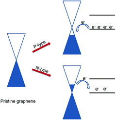 | ||
| Fig. 1 Energy band diagram after establishing contact between graphene and the photo-active molecule. | ||
3 The fabrication of device
With the development of synthetic techniques and device fabrication methods, the rational integration of nanomaterials into various hybrid nanostructures with enhanced photodetection performances has been achieved, as summarized in Table 1.| Photoactive materials | Graphene | Fabrication of hybrid material | Substrate | Doping type | Responsivity (A W−1) | Detectivity (Jones) | Maximum absorption wavelength (nm) | Determined wavelength (nm) | Ref. | |
|---|---|---|---|---|---|---|---|---|---|---|
| Rhodamine derivatives | R6G | Exfoliated graphene | Dip-pen nanolithography (DPN) | Si/SiO2 | n | — | — | — | — | 33 |
| R6G | CVD | Drop-casting | Si/SiO2 (ODTS) | p | ∼460 | 1016 | 530 | 400–980 | 34 | |
| Rh110 | CVD | Dip-coating | p | 283 | 490 | 35 | ||||
| Rh101 | CVD | Dip-coating | n | 455 | 565 | |||||
| Rh800 | CVD | Dip-coating | p | 1031 | 685 | |||||
| Rh110/Rh101/Rh800 | CVD | Drop-casting | 103 | 1010 | — | <760 | ||||
| Self-assembly | D–A type molecule | CVD | — | — | — | — | — | 740 | 710 | 44 |
| CVD | Spin-casting | ITO/PEDOT:PSS | — | — | — | — | — | |||
| ml-C8-BTBT | CVD | CVD | Si/SiO2 | p | 1.57 × 10⁴ | — | 360 | 355 | 42 | |
| fl-C8-BTBT | CVD | CVD | 4.76 × 10⁵ | — | ||||||
| Tetraphenyl-porphyrin (H2TPP) | H2TPP | CVD | Thermal evaporation (TE) | Si/SiO2 (PET) | n | 0.22 | — | — | — | 43 |
| ZnTPP | CVD | p | 0.54 | — | — | — | ||||
| AlTPP | CVD | 5.36 | — | — | — | |||||
| Ruthenium polypyridyl | Ru-Complex | CVD | Dip-coating | Si/SiO2 | n | 105 | — | — | — | 37 |
| P3HT | P3HT/graphene/TiOx | CVD | Spin-coating | Si/SiO2 | p | — | — | — | — | 36 |
| Spiropyran/merocyanine | Spiropyran | CVD | Dip-coating | Si/SiO2 | n | — | — | 560 | — | 38 |
| CVD | Spin-coating | Si/SiO2 | n | — | — | — | — | 39 | ||
| SWCNTs | Single-walled carbon nanotubes | Separated graphene | Dip-coating | Si/SiO2 | — | — | — | — | — | 40 |
| Biomaterials | Cytochrome c | CVD | Si/SiO2 | n | 1.39 × 10⁴/7.57 × 104 | — | — | 340, 410 | 41 | |
3.1 The choice of substrate
The type of substrate has a great effect on the performance of the device. Typically, a Si/SiO2 substrate is used when the photodetectors are fabricated, and a heavily doped Si wafer is employed as the gate electrode and a thermally grown 300 nm SiO2 layer above it acts as a gate dielectric.58–61 The carrier density, and thus the conductivity of the channel can be modulated by an electric field applied on the gate. The surface of the SiO2 dielectric can be modified with self-assembling monolayers composed of, e.g., n-octadecyltrimethoxysilane (ODTS) to decrease charge trapping caused by defects.Conventional photodetectors based on inorganic materials are usually built on rigid and planar substrates, which limits their application in flexible devices. Phototransistors based on organic–graphene hybrid materials are easy to integrate with low-temperature processable flexible substrates over large areas, for instance, polyethylene terephthalate (PET) and polyimide (PI).62–66 Because of its good mechanical flexibility, graphene finds an irreplaceable position in the fabrication of flexible devices, and hence it is clear that a substrate with flexibility plays a very important role in developing a new type of device. Ki-Seok An et al. have successfully fabricated various graphene-based photodetectors via simple and efficient vapor-phase metalation of porphyrin on PET films and facilitated the development of new architectures for flexible graphene–organic devices.43
3.2 Preparation of graphene
Both pristine graphene and chemically functionalized graphene are highly attractive for applications in optoelectronics and photoenergy conversion, due to their excellent electronic and optical properties as well as tuneable work functions.67–70 Synthesis of graphene is essential for its practical application in electronics and optoelectronics. Graphene can be obtained in different forms, and the most commonly used types are the exfoliated graphene layers71–75 and graphene grown by the chemical vapor deposition (CVD) method on various substrates.76–80The quality of graphene has a great influence on the electronic properties of hybrid materials. Mechanically exfoliated graphene is relatively clean in comparison with CVD-grown graphene and is widely used in the experimental studies of partial theoretical calculations.81–84 In addition to that, electrochemical exfoliated graphene can be easily fabricated into a large sized paper like form by applying brush painting of a concentrated graphene ink, which shows great promise for the industrial-scale synthesis of high-quality graphene for numerous advanced applications.85
In particular, a large area, high-quality graphene film grown by the chemical vapor deposition (CVD) method is more promising for extensive applications because of its flexibility, high transparency, and electrical conductivity, and most importantly due to the fact that the number of layers can be controlled by adjusting growth conditions.86,87 After the CVD graphene is separated from the metallic catalyst where it is grown, it can be easily transferred to a dielectric substrate, which is a commonly used method in device fabrication. Then using conventional photolithography and subsequent reactive ion etching (RIE) with O2 plasma etching steps, channels with a certain width can be patterned on the substrate.88–96
3.3 The choice of sensitization material
Due to its large aromatic sp2 lattice, free of dangling bonds, graphene is intrinsically chemically inert. The broad sensing potential of graphene can be activated by small molecules (such as rhodamine derivatives, C8-BTBT, tetraphenyl-porphyrin, ruthenium polypyridyl), conjugated polymers, rare-earth components and even semiconductor nanoparticles (NPs)97–99 by covalent or noncovalent functionalization. Since non-covalent modification can be realized by a solution method (such as dip-coating, spin-coating, and drop-casting methods and dip-pen nanolithography) and thermal evaporation (TE), it is easier than covalent modification, in which sensitive materials are attached to graphene by an amidation reaction,100–104 cycloaddition reaction,105–108 free radical addition,109,110 metal-catalysed coupling reactions111,112 and “click” chemistry.113–122 As there have been several review articles with regard to graphene functionalization,123–128 our focus herein is mainly on the non-covalent modification of small organic molecules on the surface of graphene.Small organic molecules are an important class of materials for photodetector applications, offering wide material selection, excellent mechanical flexibility, and self-assembly or solution manufacturing capability. Recently, combining graphene with small photoactive functional components has attracted widespread attention, and several important photo-active moieties, including porphyrin, phthalocyanine, pyrenebutyrate, rhodamine 6G and so on, have been attached either to the edge or to the basal plane of the graphene surface. Hybrid nanostructures are usually synthesized by an epitaxial or solution processing method, which is suitable for large area preparation in succession with low cost.129–135
As for small organic molecules, a solution-based procedure is a simple, yet highly efficient method for decorating a large area graphene with the lowest cost. Dip-coating, drop-casting and spin-coating are the three common solution processing methods. In the dip-coating method, graphene is directly immersed in a solution of organic molecules. First-principles density functional theory (DFT) calculations indicate that the absorption of photoactive molecules and graphene has a great relationship with dipoles, binding energy, and interfacial layer spacing between the dyes and graphene.136–142 Therefore, molecules with a high binding energy in the mixed solution have higher affinity when adsorbed with graphene, so it is difficult to control the components of organic hybridization. Compared to dip-coating, the drop-casting method can accurately control the hybrid components by direct deposition. Spin coating is one of the most common techniques for depositing thin films on substrates. It is used in a wide variety of industries and technology sectors. The advantage of spin-coating is its ability to quickly and easily produce very uniform films, ranging from a few nanometres to a few microns in thickness. The thickness and crystallinity of the active layer can be effectively adjusted by adjusting the rotation speed and concentration. Because of the simple and easy operation of the solution method, it has a good application prospect in the preparation of nanodevices.
The previously mentioned studies on organic/graphene hybrid materials mainly use the solution process without any knowledge or control of the interface quality, which could lead to severe underperformance of the phototransistors. In general, the thickness of the active layers could be well controlled with the help of CVD by tuning the evaporation temperature, growth time, and the position of the substrate. Xinran Wang and coworkers epitaxially grew C8-BTBT layers on prepatterned graphene field-effect transistors (FETs) with Au electrodes in a home-built CVD furnace to fabricate C8-BTBT/graphene hybrid organic photodetectors and studied the influence of the thickness of the active layers on the performance of devices.42
Thermal evaporation (TE) is commonly used in the deposition of electrodes. It is also a reasonable method to control the thickness of the organic layers. TE is a convenient way for follow-up processing if multiple organic layered materials are needed. Ki-Seok An et al. deposited a metal-free H2TPP/graphene hybrid layer on a substrate to fabricate a H2TPP/graphene photodetector, and then metallized the H2TPP to form ZnTPP or Al(III)TPP by using diethylzinc (DEZ) and trimethylaluminum (TMA) precursors, respectively.43
3.4 Interaction between photoactive moieties and graphene
Most non-covalent functionalizations have been carried out via π–π stacking between conjugate structures with graphene and facilitate photo-excited charge transfer between the dye molecules and graphene, which results in the photoconductive gain. The deposition of the dye molecules can be performed using a simple dip-coating method. Using this method Jeong Ho Cho et al. prepared hybrid photodetectors by soaking a prepared graphene device in a mixture of three different dye molecules and then rinsing with deionized water.35 Interestingly, the spectra of the mixed hybrid films fabricated using this process showed only the Rh800 spectrum due to the higher affinity of Rh800 dyes to the graphene surface. However, the drop-casting and spin-coating processes enabled the adsorption of molecules (Rh101 and Rh110) having weak binding energies with graphene. The amount of sensitization molecules can be controlled through these processes, thereby adjusting the performance of the device.4 The progress of organic–graphene hybrid photodetectors
4.1 Hybrid layer prepared by the solution method
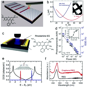 | ||
| Fig. 2 (a) Schematic illustration depicting the patterning of rhodamine 6G (R6G) on graphene by dip-pen nanolithography (DPN). The inset shows the chemical structure of R6G. (b) IDS–VG curves of the same graphene device (shown in the inset; the gold contact was prepared by evaporation of gold through a shadow mask) before (red) and after (blue) bulk functionalization with R6G. The bias voltage applied is 1 mV for both measurements. The Dirac point moved from ∼32 to ∼−6 V. Copyright 2013, Nano Lett.33 (c) Schematic diagram and optical microscopy top-view images of the dye sensitized graphene photodetector. (d) Responsivity (R) and external quantum efficiency (EQE) as a function of the illumination power. The inset shows the photocurrent at VG = 0V as a function of the illumination power. (e) Calculated joint density of states (DOS) of the graphene–R6G hybrid structure. The black line represents the DOS of the graphene. The positions of the HOMO (blue) and LUMO (red) levels were obtained from B3PW91 calculations of the physiosorbed R6G molecule. The HOMO of this structure was located at −0.971 eV and the LUMO was located at 1.150 eV with respect to the location of the Dirac point of graphene. (f) UV-IR absorption spectra of R6G and R6G/graphene hybrid films. The red line was arbitrarily shifted upward to distinguish the absorbance of R6G from that of the R6G/graphene hybrid films. Copyright 2015, Carbon.34 | ||
Encouraged by the above results, Jeong Ho Cho and coworkers developed a hybrid structure comprising organic dye molecules (e.g., rhodamine 6G) and graphene for the realization of high-performance optoelectronic devices (Fig. 2c).34 The dye-sensitized photodetectors respond to the incident illumination over a broad wavelength range (400 < k < 1000 nm), as well as with a high responsivity (∼460 A W−1 at illumination power of 1 μW) (Fig. 2d). The photocurrent generated in the hybrid photodetector (on the order of mA) is much higher than that generated in a pristine graphene photodetector (on the order of μA). This hybrid graphene photodetector displays several advantages over other approaches: the device could operate at low voltages and the photoresponse does not vary significantly across the detector area. Apart from that, they find that both pristine R6G and the hybrid system display an absorption peak at ∼530 nm corresponding to the direct transition from the HOMO to the LUMO of R6G, which means the adsorption of R6G does not change (Fig. 2e and f). This work provides a good demonstration for designing and preparing graphene photodetectors sensitized with dye molecules to realize wavelength selective detection properties.
Based on the above work, Jeong Ho Cho and coworkers systematically investigated hybrid structures of organic dyes and graphene for the fabrication of photodetectors that display spectral color selectivity.35 Rh110, Rh101 and Rh800 with blue, green and red absorption profiles were deposited onto a graphene surface by dip-coating (Fig. 3a). The photodetectors based on the three different dye–graphene hybrid films exhibited the expected spectral color selectivities and maximum photocurrents were observed at wavelengths corresponding to the maximum absorption peak positions of each dye molecule (Fig. 3b and c). Herein, in order to broaden the spectral bandwidth over the full-color range, a resulting solution, consisting of Rh110, Rh101 and Rh800, is deposited onto a graphene channel (Fig. 3d). The mixed hybrid films exhibited a wide absorption spectral bandwidth that covered the absorption spectral ranges of each dye molecule (Fig. 3e). The mixed organic dye hybrid photodetectors offer spectral color selectivities with a high responsivity of 103 A W−1 and a detectivity of ≈1010 Jones at an illumination power of 10 nW. The hybrid system of graphene/organic dyes represents a versatile platform for the development of graphene-based optoelectronic devices.
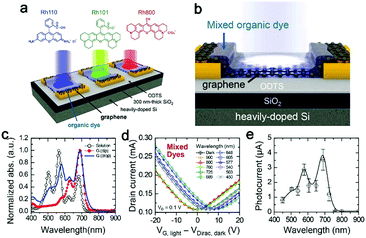 | ||
| Fig. 3 (a) Schematic illustration of an organic dye–graphene hybrid photodetector based on three different rhodamine-based dye molecules (Rh110: blue, Rh 101: green, and Rh800: red). The upper panel shows the chemical structures of the organic dyes used in this study. (b) Schematic illustration of the organic dye-graphene hybrid photodetector based on the mixture of dye molecules. (c) UV-vis absorption spectra of the mixed dye solutions and films fabricated using the dip-coating and drop-casting methods. (d) IDversus (VG,light–VDirac,dark) plots of the hybrid photodetectors based on the mixed dyes under different illumination wavelengths at a fixed incident illumination power of 1 μW. (e) Photocurrents at the Dirac voltages in the hybrid photodetectors. Copyright 2016, Advanced Functional Materials.35 | ||
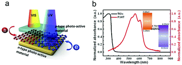 | ||
| Fig. 4 (a) A proposed device structure with wavelength-selective n- and p-type doping, consisting of a graphene transistor sandwiched between one UV- and one visible-light-sensitized photoactive layer. (b) The complementary UV-vis absorption spectra of the organic polymer P3HT and inorganic TiOx thin films of the OIHD platform. The inset shows the corresponding energy levels of graphene based on the OIHD platform. Copyright 2015, Advanced Materials.36 | ||
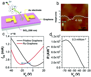 | ||
| Fig. 5 (a) Schematic depiction of a graphene–ruthenium complex hybrid FET-type photodetector. In the chemical structure of complex 1, H atoms were omitted and C, N, O, and Ru atoms are represented by gray, blue, light-red, and dark-red balls. For clarity, the scale of complex 1 is enlarged compared to graphene. (b) AFM height and surface profile (white line) along the black dotted line (ruthenium complex 1/graphene/SiO2/Si). (c) Transfer characteristics of pristine graphene and ruthenium complex 1/graphene devices (VDS = 1 V) under dark conditions. (d) Responsivity as a function of gate voltage (the wavelength of incident light: λ = 450 nm). Copyright 2014, Small.37 | ||
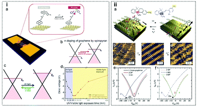 | ||
| Fig. 6 (i-a) Schematic illustration of a FET device with spiropyran functionalized graphene. (b) Energy level change of graphene after being functionalized with spiropyran. (c) Energy level change upon UV and visible light exposure. (d) Dirac point change as a function of UV and visible light exposure time. Copyright 2012, ACS Nano.38 (ii-a) Photo-switchable molecular crystals in two dimensions. A schematic representation of the approach. A spiropyran (SP) derivative forms ordered crystalline structures when deposited on different van der Waals substrates. In the cartoon, a MoS2 single layer is depicted in which the yellow (blue) layer represents the S-(Mo-) atomic plane. Photo-induced isomerization induces a structural rearrangement. The molecular dipoles (depicted as black arrows) are randomly oriented before irradiation, yet well aligned after UV irradiation, leading to a modification in the energetics of the van der Waals substrate. The chemical structure of the spiropyran (SP)–merocyanine (MC) derivative used in the study is also shown. (b–d) Scanning tunneling microscopic imaging of SP assemblies on HOPG. Height images of the molecular assemblies obtained (b) after spin-coating the SP solution, (c) immediately after UV irradiation, and (d) 48 h after UV irradiation. A schematic sketch of the molecule is superimposed onto the images to facilitate the visualization of the molecular ordering. Tunneling parameters: It = 20 pA (b, c and d), Vt = 1000 mV (b and d), 600 mV (c). Electrical characteristics of devices, (e) trace 1 (black): clean graphene, trace 2 (red): graphene covered with the SP layer, trace 3 (blue): graphene/MC after UV irradiation over the whole flake. The arrow highlights the negative shift in the threshold voltage accompanying the SP → MC isomerization, indicative of n-type doping. (f) Trace 4 (green): recovered graphene/SP after green light irradiation of the whole graphene surface. Traces 2 and 3 are replotted for clarity (dashed). Copyright Nature communication, 2018.39 | ||
At present, in the study of SP molecules, the isomerization of molecular structure is inferred based on electrical properties, without a direct, real-space visualization of the (supra)molecular structural changes induced by the switching events. However, scanning tunneling microscopy (STM) is a good way to acquire the real-space images of supramolecular assemblies of photochromic molecules. Paolo Samorì and coworkers achieved exquisite control over events taking place from the molecular level to the device scale by combining different experimental and theoretical approaches (Fig. 6ii-a).39 They designed and synthesized a spiropyran (SP) derivative bearing an 18-carbon long alkyl chain, and monitored the evolution of the molecular arrangement with sub-nm resolution by STM imaging in air and at room temperature on dry films on HOPG to study the photoswitch of the SP derivative down to the monolayer limit. As for the STM image, photochromic molecules assembled at the surface of single layer graphene generate an atomically precise superlattice in which a major structural rearrangement is obtained by light-induced collective isomerization (Fig. 6ii-b–d). As a result, the rearrangement causes a reversible shift in the work function of two-dimensional materials (2DMs), readable in devices as significant doping, which is also fully reversible (Fig. 6ii-e and f). This work offers a yet unexplored solution to supramolecular electronics, in which atomic precision in molecular self-assembly is tailored not to optimize charge transport but rather to control it by imparting new properties to a material, enabling the realization of multifunctional, high-performance devices.
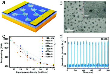 | ||
| Fig. 7 (a) Schematic illustration of a carbon-based photodetector. (b) Typical SEM images of SWCNT/SGR hybrid networks in the channel. (c) Responsivity as a function of incident power density operating at 10 V under different illumination wavelengths. (d) Transient photoresponse of the device to pulsed illumination (1064 nm, 35 mW cm−2) with a frequency of 625 Hz. Copyright Advanced Optical Materials 2018.40 | ||
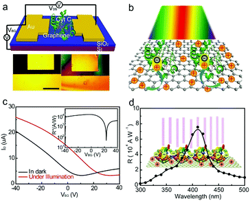 | ||
| Fig. 8 (a) Schematic image of the Cyt c/GFET heterojunction photodetector (upper). Image of a GFET channel before and after the Cyt c was printed on its channel, respectively (the scale bar is 5 μm). (b) Schematic description of the Cyt c molecules absorbing the photons under illumination and the generated excitons separated by the built-in electric field due to the band-edge alignment at the Cyt c/graphene interface. (c) IDversus VBG curves of a Cyt c/GFET heterojunction photodetector (in vacuum) measured in the dark and under illumination (340 nm, power density of 1.34 mW cm−2). Inset: Calculated photoresponsivity as a function of VBG. (d) Spectral photoresponsivity of the Cyt c/GFET heterojunction photodetectors. Inset: Scheme of interface charges after exciton dissociation. Copyright Advanced Functional Materials, 2018.41 | ||
4.2 Hybrid layer prepared by self-assembly
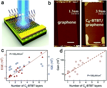 | ||
| Fig. 9 (a) Schematic illustration of a typical C8-BTBT-graphene phototransistor. (b) The AFM images of a graphene FET before (left) and after (right) C8-BTBT epitaxial growth. The device is mostly covered with IL + 1L C8-BTBT as reflected from the measured height increase by 2.6 nm. Scale bars: 2 μm. (c) EQE (red triangles) and IQE (blue squares) as a function of average number of C8-BTBT layers for all the measured devices (laser power, 100 μW cm−2). The red dashed line reflects the linear increase of EQE. (d) Photoconductive gain (Gph) as a function of average number of C8-BTBT layers for all the measured devices (laser power, 100 μW cm−2). The red dashed line reflects the exponential increase of Gph. Copyright 2016, Advanced Materials.42 | ||
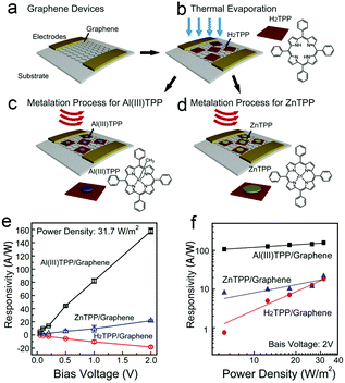 | ||
| Fig. 10 (a–d) Schematic representation of H2TPP– and metalloporphyrin–graphene hybrid film formation. (e) Photoresponsivity of H2TPP-, ZnTPP-, and Al(III)TPP-graphene-based devices as a function of the source–drain bias voltage during exposure to light with a power density of 31.7 W m−2. (f) Photoresponsivity as a function of the light power density; a bias voltage of 2 V was used for the measurements. Copyright 2016, Nanotechnology.43 | ||
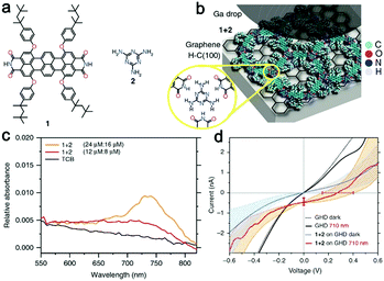 | ||
Fig. 11 (a) Structure of TDI tetracarboxylic acid derivative (1) and melamine (2). (b) Schematic drawing of the device setup including the ideal representation of the 1 + 2 mixture yielding a hexagonal supramolecular network via hydrogen bonds (yellow circle). (c) 1 + 2 (12 mM![[thin space (1/6-em)]](https://www.rsc.org/images/entities/char_2009.gif) : :![[thin space (1/6-em)]](https://www.rsc.org/images/entities/char_2009.gif) 8 mM) and pure 1,2,4-trichlorobenzene (TCB) baseline absorbance spectra. The result with the concentrations of molecules 1 and 2 increased to 24 mM 8 mM) and pure 1,2,4-trichlorobenzene (TCB) baseline absorbance spectra. The result with the concentrations of molecules 1 and 2 increased to 24 mM![[thin space (1/6-em)]](https://www.rsc.org/images/entities/char_2009.gif) : :![[thin space (1/6-em)]](https://www.rsc.org/images/entities/char_2009.gif) 16 mM is also shown as additional evidence of strong absorbance reduction upon complexation with 2. (d) Current–voltage characteristics before (black lines) and after (green lines) λ = 520 nm photon irradiation. Approach parameters: It = 2 nA and Vt = 100 mV. Striped areas indicate the maximum and minimum currents observed in more than ten curves in a single junction, while error bars indicate the standard deviation for five junctions in three samples and are reported in the main text as ISC = (0.5 ± 0.2) nA, VOC = (270 ± 120) mV. Copyright 2016, Nature Communications.44 16 mM is also shown as additional evidence of strong absorbance reduction upon complexation with 2. (d) Current–voltage characteristics before (black lines) and after (green lines) λ = 520 nm photon irradiation. Approach parameters: It = 2 nA and Vt = 100 mV. Striped areas indicate the maximum and minimum currents observed in more than ten curves in a single junction, while error bars indicate the standard deviation for five junctions in three samples and are reported in the main text as ISC = (0.5 ± 0.2) nA, VOC = (270 ± 120) mV. Copyright 2016, Nature Communications.44 | ||
In addition, Thomas P. Russell and coworkers alternately installed typical triphenylamine (TPA) as an electron-rich unit and BTTh2 (4,7-bisthienyl-2,1,3-benzothiadiazole) as an electron-deficient unit into acetylene linked conjugated macrocycles (Fig. 12).45 STM experiments confirmed that the two shape-persistent cyclic molecules showed interesting concentration-controlled self-assembling behaviour at the solid/liquid interface and could capture fullerenes within their inner cavities to form host–guest coassembly structures. Moreover, in the new stable complexes, D–A conjugated cyclic molecules act as donors and fullerene (C70) as an acceptor to form new donor–acceptor heterojunctions with big shape complementarity D/A molecular interfaces. More importantly, this work provides further opportunities to achieve high-efficiency organic solar cells through utilizing D–A conjugated cyclic molecules as donor materials with PCBM to control the morphology of the active layer.
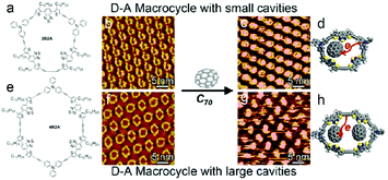 | ||
| Fig. 12 (a and e) The chemical structure of two conjugated D–A macrocycles. (b and f) STM image of the molecular self-assembly structure at the HOPG/1-phenyloctane interface under certain solution concentrations. (c and g) STM images of the coassembly structure of 3B2A and 4B2A with C70 respectively at the HOPG/1-phenyloctane interface and their corresponding calculated models (d and h). Copyright ACS Nano, 2017.45 | ||
4.3 Covalent organic frameworks (COFs)
Covalent organic frameworks (COFs), consisting of molecular building blocks connected by covalent bonds, are a new class of porous architectures that allow the integration of organic units with atomic precision into long-range-ordered two- or three-dimensional structures.195–203 Owing to the covalent linkage of the components, as well as the elaborately controlled structure, including the nature of the structural unit molecule, COFs are promising for photodetectors. Theoretical calculations have predicted the attractive properties of 2D conjugated polymers for more than two decades.204 In fact, the Jiang group has already explored the photoelectric properties of bulk COFs in recent years. They show that metallophthalocyanine, porphyrin and its self-assembly materials have great potential in photoelectric devices.205–207 However, the poor dispersibility of bulk COFs is the major drawback in their optoelectronic applications.2D COFs with layered structures stacked together through van der Waals interactions are ideally suited for efficient energy storage and charge transport. The surface confined synthesis on single-crystal surfaces is a simple while efficient methodology for the preparation of 2D COFs with single layer thickness, and easy control of the number of layers, as well as the bandgap. Lei and coworkers designed a simple while efficient methodology for the preparation of 2D COFBTA–PDA at an octanoic acid/graphene interface.46 As the synthesized 2D COF film is adsorbed on graphene, there is a strong coupling between surface COFBTA–PDA and graphene, which was revealed by the contrast of surface COFBTA–PDA on different parts of the graphene surface (Fig. 13a and b). The shape of the density of states (DOS) of the G-surface COFBTA–PDA near the Fermi level is dominated by graphene and the band gap of the G-surface COFBTA–PDA complex is very small (0.081 eV), which indicate that the imine based surface COFs are intriguing two dimensional organic semiconductors with a tuneable band gap (Fig. 13c and d). It provides a potential technological approach to sensitize graphene with 2D COFs with controllable thickness for applications in flexible devices.
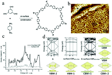 | ||
| Fig. 13 (a) Reaction scheme of Schiff base condensation between benzene-1,3,5-tricarbaldehyde (BTA) and p-phenylenediamine (PDA) into hexagonal 2D surface COFBTA–PDA. (b) STM image of surface COFBTA–PDA on SLG-copper (single layer graphene grown by CVD on copper). A “5 + 7” defect is highlighted by an overlaid schematic model and two typical domain boundaries are marked by the white arrows. A perfect chain of hexagons crossing the step edge of copper is marked by a black arrow. (c) Density of states of G-surface COFBTA–PDA (the surface of COFBTA–PDA–graphene complex) and surface COFBTA–PDA (Fermi level is set at 0 eV). (d) The band structures of graphene, surface COFBTA–PDA, G-surface COFBTA–PDA and the decomposed charge density of G-surface COFBTA–PDA near the Fermi level (Fermi level is set at 0 eV). Copyright 2014, Angewandte Chemie International Edition.46 | ||
5 Conclusion and perspectives
Graphene, a single layer 2D structure, possesses excellent physical and chemical properties, such as high mobility and thermal conductivity, great mechanical strength and extremely large specific surface area. However, pristine graphene shows a limited application in photodetectors because of its low optical absorption and zero band gap. In order to improve the performance of graphene-based photodetectors, a series of methods have been used to achieve high-quality photodetection, including both device geometry and materials engineering.Over the past few decades, the booming of studies on developing chemically functionalized graphene created great opportunities for the development of hybrid thin film transistors, and numerous dramatic and unprecedented results are demonstrated in front of the world, including many excellent results using photo-active moieties to functionalize graphene. In this article, we have systematically introduced the application of graphene functionalized with organic molecules in photodetectors in three progressive parts: the gain mechanism in optical gain, the integration of device and the progress in applications of hybrid films in photodetectors. Based on these contents, it is worth noting that the aforementioned graphene hybrid nanostructures will play an important role in improving the performance and extending the function of traditional photodetectors.
Although many successful examples have been demonstrated, large-scale, practical applications of graphene-based hybrid materials in photodetection and photodetectors still have a long way to go. Furthermore, in order to achieve the preparation of a graphene-based photodetector with a large area, stable performance and commercial application, there are still some problems that should be optimized. Firstly, how to produce high-quality, large-area, low-defect (structure defects or oxidation sites) graphene or graphene sheets is still a challenge in the preparation and improvement of photodetectors and to go into the mechanism of graphene-based photodetectors. Therefore, new methodologies for milder exfoliation and chemical modification of graphene are still needed to tackle this problem. Secondly, since graphene cannot directly generate long-lived charge carriers208 in photoelectron light energy conversion applications, it is necessary to make more carefully designs of chemical functionalization and linking groups, in order to take advantage of the electronic interaction between graphene and photoactive groups.209,210 Multi-functionalized graphene materials with different small organic molecules are expected to provide new ideas for designing charge transfer systems for light energy conversion. Moreover, with the development of nanotechnology, integrated nanosystems and multifunction circuits have attracted much research attention due to their potential applications in many fields. Thus, the development of integratable nanophotodetectors is highly needed.
For many types of detectors, performance parameters have already been demonstrated at levels that are superior or on a par with existing technologies. To move forward, the ultrahigh photoresponsivity or ultrafast response speed of graphene-based photodetectors is still a challenge to have them both in a single device. This is a prerequisite for graphene-based photodectors to realize commercialization. In addition, the prospect of commercialization depends not only on the performance of the detectors, but also on their unique strengths and capabilities, as well as the ability to achieve large-scale, high-quality GRM production at low cost, and the creation of large-energy and long-lived photons and integration of electronic platforms such as CMOS technology.
Conflicts of interest
There are no conflicts to declare.Acknowledgements
This work was supported by the National Science Foundation of China (21572157, 21872103, 51633006) and the Ministry of Science and Technology of China (Grants 2016YFB0401100).Notes and references
- E. H. Hwang, S. Adam and S. Das Sarma, Phys. Rev. Lett., 2007, 98, 186806 CrossRef CAS PubMed.
- F. Schedin, A. K. Geim, S. V. Morozov, E. W. Hill, P. Blake, M. I. Katsnelson and K. S. Novoselov, Nat. Mater., 2007, 6, 652 CrossRef CAS PubMed.
- R. R. Nair, P. Blake, A. N. Grigorenko, K. S. Novoselov, T. J. Booth, T. Stauber, N. M. R. Peres and A. K. Geim, Science, 2008, 320, 1308 CrossRef CAS PubMed.
- S. Pang, Y. Hernandez, X. Feng and K. Müllen, Adv. Mater., 2011, 23, 2779 CrossRef CAS PubMed.
- K. Nomura and A. H. MacDonald, Phys. Rev. Lett., 2006, 96, 256602 CrossRef PubMed.
- C. M. Weber, D. M. Eisele, J. P. Rabe, Y. Liang, X. Feng, L. Zhi, K. Müllen, J. L. Lyon, R. Williams, D. A. V. Bout and K. J. Stevenson, Small, 2010, 6, 184 CrossRef CAS PubMed.
- M. L. Müeller, X. Yan, B. Dragnea and L. Li, Nano Lett., 2011, 11, 56 CrossRef PubMed.
- P. Plochocka, P. Kossacki, A. Golnik, T. Kazimierczuk, C. Berger, W. A. de Heer and M. Potemski, Phys. Rev. B: Condens. Matter Mater. Phys., 2009, 80, 245415 CrossRef.
- Y. Yang and R. Murali, Appl. Phys. Lett., 2011, 98, 093116 CrossRef.
- K. K. Manga, J. Wang, M. Lin, J. Zhang, M. Nesladek, V. Nalla, W. Ji and K. P. Loh, Adv. Mater., 2012, 24, 1697 CrossRef CAS PubMed.
- S. Ryu, L. Liu, S. Berciaud, Y. Yu, H. Liu, P. Kim, G. W. Flynn and L. E. Brus, Nano Lett., 2010, 10, 4944 CrossRef CAS PubMed.
- H. Xu, Y. Chen, J. Zhang and H. Zhang, Small, 2012, 8, 2833 CrossRef CAS PubMed.
- F. Schedin, A. K. Geim, S. V. Morozov, E. W. Hill, P. Blake, M. I. Katsnelson and K. S. Novoselov, Nat. Mater., 2007, 6, 652 CrossRef CAS PubMed.
- X. Dong, D. Fu, W. Fang, Y. Shi, P. Chen and L.-J. Li, Small, 2009, 5, 1422 CrossRef CAS PubMed.
- A. K. Geim, Science, 2009, 324, 1530 CrossRef CAS PubMed.
- W. Wei and X. Qu, Small, 2012, 8, 2138 CrossRef CAS PubMed.
- I. Gierz, C. Riedl, U. Starke, C. R. Ast and K. Kern, Nano Lett., 2008, 8, 4603 CrossRef CAS PubMed.
- K. S. Novoselov, A. K. Geim, S. V. Morozov, D. Jiang, Y. Zhang, S. V. Dubonos, I. V. Grigorieva and A. A. Firsov, Science, 2004, 306, 666 CrossRef CAS PubMed.
- P. Plochocka, P. Kossacki, A. Golnik, T. Kazimierczuk, C. Berger, W. A. de Heer and M. Potemski, Phys. Rev. B: Condens. Matter Mater. Phys., 2009, 80, 245415 CrossRef.
- K. K. Manga, J. Wang, M. Lin, J. Zhang, M. Nesladek, V. Nalla, W. Ji and K. P. Loh, Adv. Mater., 2012, 24, 1697 CrossRef CAS PubMed.
- H. Xu, Y. Chen, J. Zhang and H. Zhang, Small, 2012, 8, 2833 CrossRef CAS PubMed.
- M. L. Müeller, X. Yan, B. Dragnea and L. Li, Nano Lett., 2011, 11, 56 CrossRef PubMed.
- M. Gobbi, E. Orgiu and P. Samorì, Adv. Mater., 2018, 30, 1706103 CrossRef PubMed.
- H. Geng, D. Yuan, Z. Yang, Z. Tang, X. Zhang, K. Yang and Y. Su, J. Mater. Chem. C, 2019, 7, 11056 RSC.
- W. J. Yu, Y. Liu, H. Zhou, A. Yin, Z. Li, Y. Huang and X. Duan, Nat. Nanotechnol., 2013, 8, 952–958 CrossRef CAS PubMed.
- H. Tan, Y. Fan, Y. Zhou, Q. Chen, W. Xu and J. H. Warner, ACS Nano, 2016, 10, 7866–7873 CrossRef CAS PubMed.
- L. Britnell, R. M. Ribeiro, A. Eckmann, R. Jalil, B. D. Belle, A. Mishchenko, Y.-J. Kim, R. V. Gorbachev, T. Georgiou, S. V. Morozov, A. N. Grigorenko, A. K. Geim, C. Casiraghi, A. H. Castro Neto and K. S. Novoselov, Science, 2013, 340, 1311–1314 CrossRef CAS PubMed.
- Z. Sun, Z. Liu, J. Li, G. Tai, S. Lau and F. Yan, Adv. Mater., 2012, 24, 5878–5883 CrossRef CAS PubMed.
- G. Konstantatos, M. Badioli, L. Gaudreau, J. Osmond, M. Bernechea, F. P. G. Arquer, F. Gatti and F. H. L. Koppens, Nat. Nanotechnol., 2012, 7, 363–368 CrossRef CAS PubMed.
- Z. Xia, P. Li, Y. Wang, T. Song, Q. Zhang and B. Sun, ACS Appl. Mater. Interfaces, 2015, 7, 24136–24141 CrossRef CAS PubMed.
- C. Teng, D. Xie, M. Sun, S. Chen, P. Yang and Y. Sun, ACS Appl. Mater. Interfaces, 2016, 8, 31289–31294 CrossRef CAS PubMed.
- Z. Tan, Y. Wu, H. Hong, J. Yin, J. Zhang, L. Lin, M. Wang, X. Sun, L. Sun, Y. Huang, K. Liu, Z. Liu and H. Peng, J. Am. Chem. Soc., 2016, 138, 16612–16615 CrossRef CAS PubMed.
- G. Zhou, S. He, K. A. Brown, J. Mendez-Arroyo, F. Boey and C. A. Mirkin, Nano Lett., 2013, 13, 1616–1621 CrossRef PubMed.
- Y. Lee, S. Yu, J. Jeon, H. Kim, J. Y. Lee, H. Kim, J. H. Ahn, E. Hwang and J. H. Cho, Carbon, 2015, 88, 165–172 CrossRef CAS.
- Y. S. Gim, Y. Lee, S. Kim, S. Hao, M. S. Kang, W. J. Yoo, H. Kim, C. Wolverton and J. Ho Cho, Adv. Funct. Mater., 2016, 26, 6593–6600 CrossRef CAS.
- P. Ho, S. Li, Y. Liou, C. Wen, Y. Chung and C. Chen, Adv. Mater., 2015, 27, 282–287 CrossRef CAS PubMed.
- X. Liu, E. K. Lee and J. H. Oh, Small, 2014, 10, 3700–3706 CrossRef CAS PubMed.
- A. Jang, E. Jeon, D. Kang, G. Kim, B. S. Kim, D. J. Kang and H. S. Shin, ACS Nano, 2012, 6, 9207–9213 CrossRef CAS PubMed.
- M. Gobbi, S. Bonacchi, J. Lian, A. Vercouter, S. Bertolazzi, B. Zyska, M. Timpel, R. Tatti, Y. Olivier, S. Hecht, M. V. Nardi, D. Beljonne, E. Orgiu and P. Samori, Nat. Commun., 2018, 9, 2661 CrossRef PubMed.
- B. Cai, Y. Su, Z. Tao, J. Hu, C. Zou, Z. Yang and Y. Zhang, Adv. Opt. Mater., 2018, 6, 1800791 CrossRef.
- M. Gong, P. Adhikari, Y. Gong, T. Wang, Q. Liu, B. Kattel, W. Ching, W. Chan and J. Wu, Adv. Funct. Mater., 2018, 28, 1704797 CrossRef.
- X. Liu, X. Luo, H. Nan, H. Guo, P. Wang, L. Zhang, M. Zhou, Z. Yang, Y. Shi, W. Hu, Z. Ni, T. Qiu, Z. Yu, J. Xu and X. Wang, Adv. Mater., 2016, 28, 5200–5205 CrossRef CAS PubMed.
- S. J. Kim, W. Song, S. Kim, M. S. Myung, S. S. Lee, J. Lim and K. An, Nanotechnology, 2016, 27, 075709 CrossRef PubMed.
- S. Wieghold, J. Li, P. Simon, M. Krause, Y. Avlasevich, C. Li, J. A. Garrido, U. Heiz, P. Samorì, K. Müllen, F. Esch, J. V. Barth and C. A. Palma, Nat. Commun., 2016, 7, 10700 CrossRef CAS PubMed.
- S. Zhang, Z. Liu, W. Fu, F. Liu, C. Wang, C. Sheng, Y. Wang, K. Deng, Q. Zeng, L. Shu, J. Wan, H. Chen and T. Russell, ACS Nano, 2017, 11, 11701–11713 CrossRef CAS PubMed.
- L. Xu, X. Zhou, W. Tian, T. Gao, Y. Zhang, S. Lei and Z. Liu, Angew. Chem., Int. Ed., 2014, 53, 9564–9568 CrossRef CAS PubMed.
- A. H. Castro Neto, F. Guinea, N. M. R. Peres, K. S. Novoselov and A. K. Geim, Rev. Mod. Phys., 2009, 81, 109 CrossRef CAS.
- F. Bonaccorso, Z. Sun, T. Hasan and A. C. Ferrari, Nat. Photonics, 2010, 4, 611 CrossRef CAS.
- K. S. Kim, Y. Zhao, H. Jang, S. Y. Lee, J. M. Kim, J. H. Ahn, P. Kim, J. Y. Choi and B. H. Hong, Nature, 2009, 457, 706 CrossRef CAS PubMed.
- F. Xia, T. Mueller, Y. Lin, A. V. Garcia and P. Avouris, Nat. Nanotechnol., 2009, 4, 839 CrossRef CAS PubMed.
- M. Breusing, C. Ropers and T. Elsaesser, Phys. Rev. Lett., 2009, 102, 086809 CrossRef PubMed.
- G. Konstantatos, M. Badioli, L. Gaudreau, J. Osmond, M. Bernechea, F. P. G. de Arquer, F. Gatti and F. H. L. Koppens, Nat. Nanotechnol., 2012, 7, 363–368 CrossRef CAS PubMed.
- T. Ohta, A. Bostwick, T. Seyller, K. Horn and E. Rotenberg, Science, 2006, 313, 951–954 CrossRef CAS PubMed.
- H. Chang, J. Cheng, X. Liu, J. Gao, M. Li, J. Li, X. Tao, F. Ding and Z. Zheng, Chem. – Eur. J., 2011, 17, 8896–8903 CrossRef CAS PubMed.
- S. H. Yu, Y. Lee, S. K. Jang, J. Kang, J. Jeon, C. Lee, J. Y. Lee, H. Kim, E. Hwang and S. Lee, ACS Nano, 2014, 8, 8285 CrossRef CAS PubMed.
- A. Rose, Concepts in Photoconductivity and Allied Problems, Robert E. Krieger Publishing, 1978 Search PubMed.
- C. Wang, X. Ren, C. Xu, B. Fu, R. Wang, X. Zhang, R. Li, H. Li, H. Dong, Y. Zhen, S. Lei, L. Jiang and W. Hu, Adv. Mater., 2018, 30, 1706260 CrossRef PubMed.
- Y. Wu, P. Liu, B. S. Ong, T. Srikumar, N. Zhao, G. Botton and S. Zhu, Appl. Phys. Lett., 2005, 86, 142102 CrossRef.
- M. Shkunov, R. Simms, M. Heeney, S. Tierney and I. McCulloch, Adv. Mater., 2005, 17, 2608–2612 CrossRef CAS.
- K. Nakayama, Y. Hirose, J. Soeda, M. Yoshizumi, T. Uemura, M. Uno, W. Li, M. J. Kang, M. Yamagishi, Y. Okada, E. Miyazaki, Y. Nakazawa, A. Nakao, K. Takimiya and J. Takeya, Adv. Mater., 2011, 23, 1626–1629 CrossRef CAS PubMed.
- Y. Liu, K. He, G. Chen, W. R. Leow and X. Chen, Chem. Rev., 2017, 117, 12893–12941 CrossRef CAS PubMed.
- Z. Liu, J. Xu, D. Chen and G. Shen, Chem. Soc. Rev., 2015, 44, 161–192 RSC.
- D. J. Lipomi, Adv. Mater., 2016, 28, 4180–4183 CrossRef CAS PubMed.
- J. Pu, Y. Yomogida, K. Liu, L. Li, Y. Iwasa and T. Takenobu, Nano Lett., 2012, 12, 4013–4017 CrossRef CAS PubMed.
- H. Yang, W. R. Leow and X. Chen, Small Methods, 2018, 2, 1700259 CrossRef.
- Y. Zhang, T. Tang, C. Girit, Z. Hao, M. Martin, A. Zettl, M. Crommie, Y. Shen and F. Wang, Nature, 2009, 459, 820–823 CrossRef CAS PubMed.
- Z. Li, E. A. Henriksen, Z. Jiang, Z. Hao, M. C. Martin, P. Kim, H. Stormer and D. N. Basov, Nat. Phys., 2008, 4, 532–535 Search PubMed.
- F. Wang, Y. Zhang, C. Tian, C. Girit, A. Zettl, M. Crommie and Y. Shen, Science, 2008, 320, 206–209 CrossRef CAS PubMed.
- W. Knap, V. Kachorovskii, Y. Deng, S. Rumyantsev, J. Lu, R. Gaska, M. S. Shur, G. Simin, X. Hu, M. A. Khan, C. A. Saylor and L. C. Brunel, J. Appl. Phys., 2002, 91, 9346 CrossRef CAS.
- G. Konstantatos, M. Badioli, L. Gaudreau, J. Osmond, M. Bernechea, F. P. G. de Arquer, F. Gatti and F. H. L. Koppens, Nat. Nanotechnol., 2012, 7, 363–368 CrossRef CAS PubMed.
- K. Roy, M. Padmanabhan, S. Goswami, T. P. Sai, G. Ramalingam, S. Raghavan and A. Ghosh, Nat. Nanotechnol., 2013, 8, 826–830 CrossRef CAS PubMed.
- L. Prechtel, L. Song, D. Schuh, P. Ajayan, W. Wegscheider and A. Holleitner, Nat. Commun., 2012, 3, 646 CrossRef PubMed.
- M. Freitag, T. Low and P. Avouris, Nano Lett., 2013, 13, 1644–1648 CrossRef CAS PubMed.
- E. Stern, J. F. Klemic, D. A. Routenberg, P. N. Wyrembak, D. B. Turner-Evans, A. D. Hamilton, D. A. LaVan, T. M. Fahmy and M. A. Reed, Nature, 2007, 445, 519 CrossRef CAS PubMed.
- A. Reina, X. Jia, J. Ho, D. Nezich, H. Son, V. Bulovic, M. S. Dresselhaus and J. Kong, Nano Lett., 2009, 9, 30–35 CrossRef CAS PubMed.
- X. S. Li, W. Cai, J. H. An, S. Kim, J. Nah, D. Yang, R. Piner, A. Velamakanni, I. Jung, E. Tutuc, S. K. Banerjee, L. Colombo and R. S. Ruoff, Science, 2009, 324, 1312–1314 CrossRef CAS PubMed.
- L. Liu, H. Zhou, R. Cheng, Y. Chen, Y. Lin, Y. Qu, J. Bai, I. A. Ivanov, G. Liu, G. Y. Huang and X. Duan, J. Mater. Chem., 2012, 22, 1498–1503 RSC.
- H. Zhou, W. Yu, L. Liu, R. Cheng, Y. Chen, X. Huang, Y. Liu, Y. Wang, Y. Huang and X. Duan, Nat. Commun., 2013, 4, 2096 CrossRef PubMed.
- B. Radisavljevic, A. Radenovic, J. Brivio, V. Giacometti and A. Kis, Nat. Nanotechnol., 2011, 6, 147–150 CrossRef CAS PubMed.
- X. Cai, A. B. Sushkov, R. J. Suess, M. M. Jadidi, G. S. Jenkins, L. O. Nyakiti, R. L. Myers-Ward, S. Li, J. Yan, D. K. Gaskill, T. E. Murphy, H. D. Drew and M. S. Fuhrer, Nat. Nanotechnol., 2014, 9, 814–819 CrossRef CAS PubMed.
- N. M. Gabor, J. C. W. Song, Q. Ma, N. L. Nair, T. Taychatanapat, K. Watanabe, T. Taniguchi, L. S. Levitov and P. Jarillo-Herrero, Science, 2011, 334, 648–652 CrossRef CAS PubMed.
- E. J. H. Lee, K. Balasubramanian, R. T. Weitz, M. Burghard and K. Kern, Nat. Nanotechnol., 2008, 3, 486–490 CrossRef CAS PubMed.
- M. Freitag, T. Low and P. Avouris, Nano Lett., 2013, 13, 1644–1648 CrossRef CAS PubMed.
- K. Parvez, Z. Wu, R. Li, X. Liu, R. Graf, X. Feng and K. Müllen, J. Am. Chem. Soc., 2014, 136, 6083–6091 CrossRef CAS PubMed.
- K. S. Kim, Y. Zhao, H. Jang, S. Y. Lee, J. M. Kim, K. S. Kim, J. H. Ahn, P. Kim, J. Y. Choi and B. H. Hong, Nature, 2009, 457–706 Search PubMed.
- X. Li, W. Cai, J. An, S. Kim, J. Nah, D. Yang, R. Piner, A. Velamakanni, I. Jung, E. Tutuc, S. K. Banerjee, L. Colombo and R. S. Ruoff, Science, 2009, 324, 1312 CrossRef CAS PubMed.
- X. Li, C. W. Magnuson, A. Venugopal, R. M. Tromp, J. B. Hannon, E. M. Vogel, L. Colombo and R. S. Ruoff, J. Am. Chem. Soc., 2011, 133, 2816 CrossRef CAS PubMed.
- Z. Sun, Z. Yan, J. Yao, E. Beitler, Y. Zhu and J. M. Tour, Nature, 2010, 468, 549 CrossRef CAS PubMed.
- A. Guermoune, T. Chari, F. Popescu, S. S. Sabri, J. Guillemette, H. S. Skulason, T. Szkopek and M. Siaj, Carbon, 2011, 49, 4204 CrossRef CAS.
- Y. Gamo, A. Nagashima, M. Wakabayashi, M. Terai and C. Oshima, Surf. Sci., 1997, 374, 61 CrossRef CAS.
- H. Ueta, M. Saida, C. Nakai, Y. Yamada, M. Sasaki and S. Yamamoto, Surf. Sci., 2004, 560, 183 CrossRef CAS.
- S. Marchini, S. Günther and J. Wintterlin, Phys. Rev. B: Condens. Matter Mater. Phys., 2007, 76, 075429 CrossRef.
- J. Coraux, A. T. N’Diaye, C. Busse and T. Michely, Nano Lett., 2008, 8, 565 CrossRef CAS PubMed.
- R. S. Edwards and K. S. Coleman, Acc. Chem. Res., 2012, 46, 23 CrossRef PubMed.
- S. Bae, H. Kim, Y. Lee, X. Xu, J. S. Park, Y. Zheng, J. Balakrishnan, T. Lei, H. R. Kim, Y. Song, Y. J. Kim, K. S. Kim, B. Ozyilmaz, J. H. Ahn, B. Hong and S. Iijima, Nat. Nanotechnol., 2010, 5, 574 CrossRef CAS PubMed.
- Z. Sun, Z. Liu, J. Li, G. Tai, S. Lau and F. Yan, Adv. Mater., 2012, 24, 5878–5883 CrossRef CAS PubMed.
- G. Konstantatos, M. Badioli, L. Gaudreau, J. Osmond, M. Bernechea, F. Pelayo Garcia de Arquer, F. Gatti and F. H. L. Koppens, Nat. Nanotechnol., 2012, 7, 363–368 CrossRef CAS PubMed.
- C. Chiang, G. Haider, W. Tan, Y. Liou, Y. Lai, R. Ravindranath, H. Chang and Y. Chen, ACS Appl. Mater. Interfaces, 2016, 8, 466–471 CrossRef CAS PubMed.
- N. Karousis, A. S. D. Sandanayaka, T. Hasobe, S. P. Economopoulos, E. Sarantopoulou and N. Tagmatarchis, J. Mater. Chem., 2011, 21, 109 RSC.
- Y. Xu, Z. Liu, X. Zhang, Y. Wang, J. Tian, Y. Huang, Y. Ma, X. Zhang and Y. Chen, Adv. Mater., 2009, 21, 1275 CrossRef CAS.
- N. Karousis, J. Ortiz, K. Ohkubo, T. Hasobe, S. Fukuzumi, Á. Sastre-Santos and N. Tagmatarchis, J. Phys. Chem. C, 2012, 116, 20564 CrossRef CAS.
- J. Zhu, Y. Li, Y. Chen, J. Wang, B. Zhang, J. Zhang and W. J. Blau, Carbon, 2011, 49, 1900 CrossRef CAS.
- X. Zhang, X. Zhao, Z. Liu, Y. Liu, Y. Chen and J. Tian, Opt. Express, 2009, 17, 23959 CrossRef CAS PubMed.
- X. Zhang, L. Hou, A. Cnossen, A. C. Coleman, O. Ivashenko, P. Rudolf, B. J. van Wees, W. R. Browne and B. L. Feringa, Chem. – Eur. J., 2011, 17, 8957 CrossRef CAS PubMed.
- M. E. Ragoussi, J. Malig, G. Katsukis, B. Butz, E. Spiecker, G. de la Torre, T. Torres and D. M. Guldi, Angew. Chem., Int. Ed., 2012, 51, 6421 CrossRef CAS PubMed.
- F. M. Koehler and W. J. Stark, Acc. Chem. Res., 2013, 46(10), 2297–2306 CrossRef CAS PubMed.
- M. Quintana, E. Vazquez and M. Prato, Acc. Chem. Res., 2013, 46, 138 CrossRef CAS PubMed.
- E. Bekyarova, S. Sarkar, F. Wang, M. E. Itkis, I. Kalinina, X. Tian and R. C. Haddon, Acc. Chem. Res., 2013, 46, 65 CrossRef CAS PubMed.
- J. R. Lomeda, C. D. Doyle, D. V. Kosynkin, W. F. Hwang and J. M. Tour, J. Am. Chem. Soc., 2008, 130, 16201 CrossRef CAS PubMed.
- T. Umeyama, J. Mihara, N. Tezuka, Y. Matano, K. Stranius, V. Chukharev, N. V. Tkachenko, H. Lemmetyinen, K. Noda, K. Matsushige, T. Shishido, Z. Liu, K. Hirose-Takai, K. Suenaga and H. Imahori, Chem. – Eur. J., 2012, 18, 4250 CrossRef CAS PubMed.
- Q. Bao, H. Zhang, J. Yang, S. Wang, D. Y. Tang, R. Jose, S. Ramakrishna, C. T. Lim and K. P. Loh, Adv. Funct. Mater., 2010, 20, 782 CrossRef CAS.
- H. C. Kolb, M. G. Finn and K. B. Sharpless, Angew. Chem., Int. Ed., 2001, 40, 2004 CrossRef CAS PubMed.
- X. Xu, J. Chen, X. Luo, J. Lu, H. Zhou, W. Wu, H. Zhan, Y. Dong, S. Yan, J. Qin and Z. Li, Chem. – Eur. J., 2012, 18, 14384 CrossRef CAS PubMed.
- M. Castelaín, G. Martínez, P. Merino, J. Á. Martín-Gago, J. L. Segura, G. Ellis and H. J. Salavagione, Chem. – Eur. J., 2012, 18, 4965 CrossRef PubMed.
- X. Chen, A. B. Braunschweig, M. J. Wiester, S. Yeganeh, M. A. Ratner and C. A. Mirkin, Angew. Chem., Int. Ed., 2009, 48, 5178 CrossRef CAS PubMed.
- H. Wang, K. Zhou, Y. Xie, J. Zeng, N. Chai, J. Li and H. L. Zhang, Chem. Commun., 2011, 47, 5747 RSC.
- J. Iehl, R. P. de Freitas and J.-F. Nierengarten, Tetrahedron Lett., 2008, 49, 4063 CrossRef CAS.
- V. V. Rostovtsev, L. G. Green, V. V. Fokin and K. B. Sharpless, Angew. Chem., Int. Ed., 2002, 41, 2596 CrossRef CAS PubMed.
- S. Campidelli, B. Ballesteros, A. Filoramo, D. D. Diaz, G. de la Torre, T. Torres, G. M. A. Rahman, C. Ehli, D. Kiessling, F. Werner, V. Sgobba, D. M. Guldi, C. Cioffi, M. Prato and J.-P. Bourgoin, J. Am. Chem. Soc., 2008, 130, 11503 CrossRef CAS PubMed.
- H. Li, F. Cheng, A. M. Duft and A. Adronov, J. Am. Chem. Soc., 2005, 127, 14518 CrossRef CAS PubMed.
- T. Palacin, H. L. Khanh, B. Jousselme, P. Jegou, A. Filoramo, C. Ehli, D. M. Guldi and S. P. Campidelli, J. Am. Chem. Soc., 2009, 131, 15394 CrossRef CAS PubMed.
- D. R. Dreyer, S. Park, C. W. Bielawski and R. S. Ruoff, Chem. Soc. Rev., 2010, 39, 228 RSC.
- K. P. Loh, Q. Bao, P. K. Ang and J. Yang, J. Mater. Chem., 2010, 20, 2277 RSC.
- Z. Sun and H. Chang, ACS Nano, 2014, 8, 4133–4156 CrossRef CAS PubMed.
- H. Wang, Q. Wang, K. Zhou and H. Zhang, Small, 2013, 9, 1266–1283 CrossRef CAS PubMed.
- J. Li, L. Niu, Z. Zheng and F. Yan, Adv. Mater., 2014, 26, 5239–5273 CrossRef CAS PubMed.
- M. Quintana, E. Vazquez and M. Prato, Acc. Chem. Res., 2013, 46, 138 CrossRef CAS PubMed.
- P. Liu, Y. Wu, Y. Li, B. Ong and S. Zhu, J. Am. Chem. Soc., 2006, 128, 4554 CrossRef CAS PubMed.
- K. Manga, S. Wang, M. Jaiswal, Q. Bao and K. P. Loh, Adv. Mater., 2010, 22, 5265–5270 CrossRef CAS PubMed.
- T. Wakahara, P. D’Angelo, K. I. Miyazawa, Y. Nemoto, O. Ito, N. Tanigaki, D. D. C. Bradley and T. D. Anthopoulos, J. Am. Chem. Soc., 2012, 134, 7204–7206 CrossRef CAS PubMed.
- Y. Wang, Y. Li, W. Zhu, J. Liu, X. Zhang, R. Li, Y. Zhen, H. Dong and W. Hu, Nanoscale, 2016, 8, 14920–14924 RSC.
- J. Lu, C. Xu, J. Dai, J. Li, Y. Wang, Y. Lin and P. Li, Nanoscale, 2015, 7, 3396 RSC.
- K. Liu, M. Sakurai, M. Liao and M. Aono, J. Phys. Chem. C, 2010, 114, 19835 CrossRef CAS.
- L. Hu, L. Wu, M. Liao, X. Hu and X. Fang, Adv. Funct. Mater., 2012, 22, 998 CrossRef CAS.
- O. Leenaerts, B. Partoens and F. Peeters, Phys. Rev. B: Condens. Matter Mater. Phys., 2009, 79, 235440 CrossRef.
- E. K. Gross and R. M. Dreizler, Density Functional Theory, Springer Science & Business Media, New York, 2013, vol. 337 Search PubMed.
- G. Kresse and D. Joubert, Phys. Rev. B: Condens. Matter Mater. Phys., 1999, 59, 1758 CrossRef CAS.
- G. Kresse and J. Hafner, Phys. Rev. B: Condens. Matter Mater. Phys., 1993, 47, 558 CrossRef CAS PubMed.
- H. J. Monkhorst and J. D. Pack, Phys. Rev. B: Solid State, 1976, 13, 5188 CrossRef.
- X. Liu, X. Luo, H. Nan, H. Guo, P. Wang, L. Zhang, M. Zhou, Z. Yang, Y. Shi, W. Hu, Z. Ni, T. Qiu, Z. Yu, J. Xu and X. Wang, Adv. Mater., 2016, 28, 5200–5205 CrossRef CAS PubMed.
- X. Chen, X. Liu, B. Wu, H. Nan, H. Guo, Z. Ni, F. Wang, X. Wang, Y. Shi and X. Wang, Nano Lett., 2017, 17, 6391 CrossRef CAS PubMed.
- L. Gao, C. Ge, W. Li, C. Jia, K. Zeng, W. Pan, H. Wu, Y. Zhao, Y. He, J. He, Z. Zhao, G. Niu, X. Guo, F. P. G. de Arquer, E. H. Sargent and J. Tang, Adv. Funct. Mater., 2017, 27, 1702360 CrossRef.
- T. Zhang, Z. Li, J. Wang, W. Kong, G. Wu, Y. Zheng, Y. Zhao, E. Yao, N. Zhuang and L. Luo, Sci. Rep., 2016, 6, 38569 CrossRef CAS PubMed.
- K. Sekiguchi, S. Yamaguchi and T. Tahara, J. Phys. Chem. A, 2006, 110, 2601 CrossRef CAS PubMed.
- X. Liu, X. Chen, J. Yi, Z. Luo, H. Nan, H. Guo, Z. Ni, Y. Ding, S. Dai and X. Wang, Org. Electron., 2019, 64, 22 CrossRef CAS.
- D. H. Kim, J. T. Han, Y. D. Park, Y. Jang, J. H. Cho, M. Hwang and K. Cho, Adv. Mater., 2006, 18, 719–723 CrossRef CAS.
- J. N. Wilson, W. Steffen, T. G. McKenzie, G. Lieser, M. Oda, D. Neher and U. H. F. Bunz, J. Am. Chem. Soc., 2002, 124, 6830–6831 CrossRef CAS PubMed.
- H. Dong, S. Jiang, L. Jiang, Y. Liu, H. Li, W. Hu, E. Wang, S. Yan, Z. Wei, W. Xu and X. Gong, J. Am. Chem. Soc., 2009, 131, 17315–17320 CrossRef CAS PubMed.
- H. A. Um, D. H. Lee, D. U. Heo, D. S. Yang, J. Shin, H. Baik, M. J. Cho and D. H. Choi, ACS Nano, 2015, 9, 5264–5274 CrossRef CAS PubMed.
- Y. Liu, H. Dong, S. Jiang, G. Zhao, Q. Shi, J. Tan, L. Jiang, W. Hu and X. Zhan, Chem. Mater., 2013, 25, 2649–2655 CrossRef CAS.
- S. Wang, M. Kappl, I. Liebewirth, M. Müller, K. Kirchhoff, W. Pisula and K. Müllen, Adv. Mater., 2012, 24, 417–420 CrossRef CAS PubMed.
- Y. Yao, H. Dong, F. Liu, T. P. Russell and W. Hu, Adv. Mater., 2017, 29, 1701251 CrossRef PubMed.
- C. Liu, Q. Wang, H. Tian, Y. Geng and D. Yan, Polymer, 2013, 54, 2459–2465 CrossRef CAS.
- K. M. Coakley and M. D. McGehee, Chem. Mater., 2004, 16, 4533 CrossRef CAS.
- W. Ma, C. Yang, X. Gong, K. Lee and A. J. Heeger, Adv. Funct. Mater., 2005, 15, 1617 CrossRef CAS.
- J. Zhang, J. Yu, M. Jaroniec and J. Gong, Nano Lett., 2012, 12, 4584 CrossRef CAS PubMed.
- Z. K. Liu, J. H. Li, Z. H. Sun, G. A. Tai, S. P. Lau and F. Yan, ACS Nano, 2012, 6, 810 CrossRef CAS PubMed.
- A. Mukherji, B. Seger, G. Lu and L. Wang, ACS Nano, 2011, 5, 3483 CrossRef CAS PubMed.
- F. Li, B. Zhang, X. Li, Y. Jiang, L. Chen, Y. Li and L. Sun, Angew. Chem., Int. Ed., 2011, 50, 12276 CrossRef CAS PubMed.
- B. L. Feringa and W. R. Browne, Molecular Switches, Wiley-VCH, Weinheim, 2011 Search PubMed.
- A. C. Whalley, M. L. Steigerwald, X. Guo and C. Nuckolls, J. Am. Chem. Soc., 2017, 129, 12590–12591 CrossRef PubMed.
- J. M. Mativetsky, G. Pace, M. Elbing, M. A. Rampi, M. Mayor and P. Samori, J. Am. Chem. Soc., 2008, 130, 9192–9193 CrossRef CAS PubMed.
- A. J. Kronemeijer, H. B. Akkerman, T. Kudernac, B. J. van Wees, B. L. Feringa and P. W. M. Blom, Adv. Mater., 2008, 20, 1467–1473 CrossRef CAS.
- E. Margapoti, P. Strobel, M. M. Asmar, M. Seifert, J. Li, M. Sachsenhauser, O. Ceylan, C. A. Palma, J. V. Barth, J. A. Garrido, A. Cattani-Scholz, S. E. Ulloa and J. J. Finley, Nano Lett., 2014, 14, 6823–6827 CrossRef CAS PubMed.
- E. Margapoti, J. Li, O. Ceylan, M. Seifert, F. Nisic, T. L. Anh, F. Meggendorfer, C. Dragonetti, C. A. Palma, J. V. Barth and J. J. Finley, Adv. Mater., 2015, 27, 1426–1431 CrossRef CAS PubMed.
- C. Jia, A. Migliore, N. Xin, S. Huang, J. Wang, Q. Yang, S. Wang, H. Chen, D. Wang, B. Feng, Z. Liu, G. Zhang, D. Qu, H. Tian, M. A. Ratner, H. Xu, A. Nitzan and X. Guo, Science, 2016, 352, 1443–1446 CrossRef CAS PubMed.
- X. Guo, L. Huang, S. O’Brien, P. Kim and C. Nuckolls, J. Am. Chem. Soc., 2005, 127, 15045–15047 CrossRef CAS PubMed.
- J. M. Simmons, I. in, V. E. Campbell, T. J. Mark, F. Léonard, P. Gopalan and M. A. Eriksson, Phys. Rev. Lett., 2007, 98, 86802 CrossRef CAS PubMed.
- M. Kim, N. S. Safron, C. Huang, M. S. Arnold and P. Gopalan, Nano Lett., 2012, 12, 182–187 CrossRef CAS PubMed.
- A. Jang, E. K. Jeon, D. Kang, G. Kim, B. S. Kim, D. Kang and H. Shin, ACS Nano, 2012, 6, 9207–9213 CrossRef CAS PubMed.
- E. Orgiu, N. Crivillers, M. Herder, L. Grubert, M. Patzel, J. Frisch, E. Pavlica, D. T. Duong, G. Bratina, A. Salleo, N. Koch, S. Hecht and P. Samori, Nat. Chem., 2012, 4, 675–679 CrossRef CAS PubMed.
- E. Orgiu and P. Samorì, Adv. Mater., 2014, 26, 1827–1844 CrossRef CAS PubMed.
- M. Suda, R. Kato and H. M. Yamamoto, Science, 2015, 347, 743–746 CrossRef CAS PubMed.
- L. Yang, S. Wang, Q. Zeng, Z. Zhang and L. Peng, Small, 2013, 9, 1225 CrossRef CAS PubMed.
- X. He, F. Léonard and J. Kono, Adv. Opt. Mater., 2015, 3, 989 CrossRef CAS.
- T. Lei, I. Pochorovski and Z. Bao, Acc. Chem. Res., 2017, 50, 1096 CrossRef CAS PubMed.
- M. Gao, Z. Huang, B. Zeng, T. Pan, Y. Zhang, H. Peng and Y. Lin, Appl. Phys. Lett., 2015, 106, 051601 CrossRef.
- C. Liu, Y. Chang, T. B. Norris and Z. Zhong, Nat. Nanotechnol., 2014, 9, 273 CrossRef CAS PubMed.
- A. D. Bartolomeo, Phys. Rep., 2016, 606, 1 CrossRef.
- B. Cai, Y. Su, Z. Tao, J. Hu, C. Zou, Z. Yang and Y. Zhang, Adv. Opt. Mater., 2018, 6, 1800791 CrossRef.
- Y. Deng, Z. Luo, N. J. Conrad, H. Liu, Y. Gong, S. Najmaei, P. M. Ajayan, J. Luo, X. Xu and P. Ye, Nano Lett., 2005, 8, 8292 Search PubMed.
- D. Jariwala, T. J. Marks and M. C. Hersam, Nat. Mater., 2017, 16, 170 CrossRef CAS PubMed.
- W. Xia, L. Dai, P. Yu, X. Tong, W. Song, G. Zhang and Z. Wang, Nanoscale, 2017, 9, 4324 RSC.
- J. He, N. Kumar, M. Z. Bellus, H. Y. Chiu, D. He, Y. Wang and H. Zhao, Nat. Commun., 2014, 5, 5622 CrossRef CAS PubMed.
- J. He, D. He, Y. Wang and H. Zhao, Opt. Express, 2017, 25, 1949 CrossRef CAS PubMed.
- M. Gong, Q. Liu, R. Goul, D. Ewing, M. Casper, A. Stramel, A. Elliot and J. Wu, ACS Appl. Mater. Interfaces, 2017, 9, 27801 CrossRef CAS PubMed.
- Q. Liu, B. Cook, M. Gong, Y. Gong, D. Ewing, M. Casper, A. Stramel and J. Wu, ACS Appl. Mater. Interfaces, 2017, 9, 12728 CrossRef CAS PubMed.
- P. Wang, S. Liu, W. Luo, H. Fang, F. Gong, N. Guo, Z. Chen, J. Zou, Y. Huang, X. Zhou, J. Wang, X. Chen, W. Lu, F. Xiu and W. Hu, Adv. Mater., 2017, 29, 1604439 CrossRef PubMed.
- C. Xie, C. Mak, X. Tao and F. Yan, Adv. Funct. Mater., 2017, 27, 1603886 CrossRef.
- H. Cheng, G. Wang, D. Li, Q. He, A. Yin, Y. Liu, H. Wu, M. Ding, Y. Huang and X. Duan, Nano Lett., 2016, 16, 367 CrossRef CAS PubMed.
- C. A. Palma and P. Samorì, Blueprinting macromolecular electronics, Nat. Chem., 2011, 3, 431–436 CrossRef CAS PubMed.
- J. A. Theobald, N. S. Oxtoby, M. A. Phillips, N. R. Champness and P. H. Beton, Nature, 2013, 424, 1029–1031 CrossRef PubMed.
- J. A. Zerkowski, C. T. Seto and G. M. Whitesides, J. Am. Chem. Soc., 1992, 114, 5473–5475 CrossRef CAS.
- B. Zhang, M. T. Trinh, B. Fowler, M. Ball, Q. Xu, F. Ng, M. L. Steigerwald, X. Zhu, C. Nuckolls and Y. Zhong, J. Am. Chem. Soc., 2016, 138, 16426–16431 CrossRef CAS PubMed.
- A. Thomas, Angew. Chem., 2010, 122, 8506–8523 CrossRef.
- A. Thomas, Angew. Chem., Int. Ed., 2010, 49, 8328–8344 CrossRef CAS PubMed.
- X. Feng, X. Ding and D. Jiang, Chem. Soc. Rev., 2012, 41, 6010–6022 RSC.
- A. J. Doonan, D. J. Tranchemontagne, T. G. Glover, J. R. Hunt and O. M. Yaghi, Nat. Chem., 2010, 2, 235–238 CrossRef PubMed.
- N. L. Campbell, R. Clowes, L. K. Ritchie and A. I. Cooper, Chem. Mater., 2009, 21, 204–206 CrossRef CAS.
- H. Furukawa and O. M. Yaghi, J. Am. Chem. Soc., 2009, 131, 8875–8883 CrossRef CAS PubMed.
- Y. G. Zhang and S. N. Riduan, Chem. Soc. Rev., 2012, 41, 2083–2094 RSC.
- S. Wan, J. Guo, J. Kim, H. Ihee and D. Jiang, Angew. Chem., Int. Ed., 2009, 48, 5439–5442 CrossRef CAS PubMed.
- S. Wan, J. Guo, J. Kim, H. Ihee and D. Jiang, Angew. Chem., 2009, 121, 5547–5550 CrossRef.
- G. Kresse and J. Furthmuller, Phys. Rev. B: Condens. Matter Mater. Phys., 1996, 54, 11169–11186 CrossRef CAS PubMed.
- X. Feng, L. Liu, Y. Honsho, A. Saeki, S. Seki, S. Irle, Y. Dong, A. Nagai and D. Jiang, Angew. Chem., Int. Ed., 2012, 51, 2618–2622 CrossRef CAS PubMed.
- X. Ding, J. Guo, X. Feng, Y. Honsho, J. Guo, S. Seki, P. Maitarad, A. Saeki, S. Nagase and D. Jiang, Angew. Chem., Int. Ed., 2011, 50, 1289–1293 CrossRef CAS PubMed.
- X. Chen, M. Addicoat, E. Jin, L. Zhai, H. Xu, N. Huang, Z. Guo, L. Liu, S. Irle and D. Jiang, J. Am. Chem. Soc., 2015, 137, 3241–3247 CrossRef CAS PubMed.
- P. V. Kamat, J. Phys. Chem. Lett., 2011, 2, 242 CrossRef CAS.
- S. Zhu, S. Tang, J. Zhang and B. Yang, Chem. Commun., 2012, 48, 4527 RSC.
- X. Lv, Y. Huang, Z. Liu, J. Tian, Y. Wang, Y. Ma, J. Liang, S. Fu, X. Wan and Y. Chen, Small, 2009, 5, 1682 CrossRef CAS PubMed.
| This journal is © the Partner Organisations 2020 |


