DOI:
10.1039/D5RA04234H
(Paper)
RSC Adv., 2025,
15, 24612-24623
Hierarchical CuO photocathodes with cobalt doping for efficient photoelectrochemical water-splitting
Received
14th June 2025
, Accepted 8th July 2025
First published on 14th July 2025
Abstract
Hierarchical cobalt-doped copper oxide (Co/CuO) photocathodes for photoelectrochemical water splitting (PEC-WS) are an effective and promising strategy to enhance light harvesting. Here, hierarchical Co/CuO photocathodes were deposited via the effective-cost SILAR technique. Crystal structural properties of Co/CuO films were examined via X-ray diffraction (XRD). XRD results confirmed the monoclinic structure and polycrystalline nature of Co/CuO. Field emission scanning electron microscopy images display a hierarchical “flower-like” morphology with nanoscale features resembling petals. All films exhibit a relatively uniform distribution of flower-like structures. The transmittance spectra of Co-doped and undoped CuO photoelectrodes were measured to study their optical properties. Increasing the Co contents led to an optical energy band gap increase. Additionally, the applied photon to current conversion efficiency (ABPE%) and electrochemical impedance spectroscopy (EIS) are comprehensively studied. Moreover, stability and incident photon to current conversion efficiency (IPCE%) were studied for optimum photoelectrode. The CuO sample with an optimal Co dopant of 3% exhibit a maximum photocurrent density of −1.5 mA cm−2 at −0.4 V vs. RHE about triple that of pure CuO photocathode, an ABPE of 0.35% at −0.4 V vs. RHE, and outstanding electrochemical stability in alkaline medium.
1. Introduction
Developing clean energy supplies is crucial to reduce greenhouse gas emissions from fossil fuels.1 Fossil fuel supplies are diminishing at an alarming rate, raising concerns about future energy security. In this setting, the desire to move to renewable energy sources becomes clear.2 Renewable energy, such as wind, geothermal power, solar, and hydro, has the potential to be a sustainable solution.3 Adopting renewable energy can help prevent climate change, decreasing dependance on fossil fuels, and fostering a more sustainable and resilient energy system. Hydrogen is regarded as the best energy carrier, with the highest gravimetric heating value and minimal carbon emissions during combustion.4 Hydrogen can generate energy in fuel cells with only water vapor as a byproduct, removing dangerous pollutants.5 However, there are limitations to the broad use of hydrogen as an energy source, especially when it comes to transporting and storing hydrogen gas. Because hydrogen has a low density, substantial amounts of energy must be stored in huge volumes.6 Finding a suitable low-cost semiconducting photocatalyst with strong light absorption and acceptable stability in aqueous electrolytes is a truly challenging circumstance.7 Metal oxide semiconductors play an important role in many industrial applications, including photoelectrochemical and optoelectronic devices. Copper(II) oxide (CuO), also referred to as cupric oxide, has emerged in recent years as one of the most important metal oxide semiconductors.8 This is because of its many useful applications and physiochemical characteristics. It is abundant in nature, inexpensive, biocompatible, has a narrow bandgap, and is chemically stable.9 Solar cells, transistors, supercapacitors, lithium-ion batteries, photocatalysis, and gas sensors are just a few of the several applications for it.10 It is thought to be beneficial for use as a photocathode in PEC cells because of the location of its conduction band edge, which is at a potential greater than that of hydrogen evolution.11 In order to increase stability and conductivity, a lot of studies have been conducted using catalysts, doping procedures, composite architectures, and other techniques. It is thought that the doping procedure is quick, easy, and efficient and it can also enhance the properties of CuO.12,13
In recent years, copper oxide (CuO) has emerged as a promising p-type semiconductor for photoelectrochemical (PEC) water splitting due to its narrow band gap (∼1.2–1.9 eV), high absorption coefficient, and earth-abundant, low-cost nature.14 CuO's conduction band is suitably positioned for hydrogen evolution, making it a viable candidate for photocathodic applications.15 However, its practical application is limited by factors such as short minority carrier diffusion lengths, rapid surface recombination, and photocorrosion.16 To enhance the material's qualities, numerous researchers have experimented with different dopant molecules. J. Uddin et al. using the spray pyrolysis technique they synthesized undoped and Ni-doped CuO thin films to study how the Ni contents affect the electrical and optical characteristics of CuO films. Ni dopants have been reported to increase resistivity and the energy band gap.17 Ba-doped CuO films were created by Ashour M. Ahmed et al. using the SILAR technique for hydrogen production. Nevertheless, the stability curve indicates that after 50 seconds, the photocurrent density drops to roughly 45% of its original value.8 Moreover, CuO thin films were created by S. Dolai et al. for solar cell applications using reactive DC magnetron sputtering. An efficiency of 1.2% and a current density of roughly 3.6 mA cm−2 have been demonstrated by the CuO/CdS p–n junction solar cell.18 Sol–gel combustion was used by S. Al-Amri et al. to create Ni-doped CuO films for optical and structural analysis. The bandgap energy of Ni-doped CuO increased significantly with the Ni content.19 Y.-F. Lim et al. used the sol–gel technique to deposit CuO and Cu2O films for PEC water splitting. −0.47 mA cm−2 was recorded as a maximum photocurrent density, and CuO and Cu2O films corroded.20 To the best of our knowledge, Co/CuO films especially prepared by SILAR method on FTO coated glass substrate have never been deposited for using in PEC water splitting. CuO thin films can be deposited using a variety of methods, such as magnetron sputtering,21 sol–gel,22 chemical bath deposition,23 spray pyrolysis,24 potentiodynamic technique,25 and SILAR technique.8 SILAR distinguishes notably among these methods due to its low cost, ease of use, speed, and suitability for large-scale production with a high-quality coating at low temperatures. In this work, we investigate how doping CuO with a rare earth ion Co2+ with an ionic radius of 0.70 Å (ref. 26) approximately similar to Cu2+ (0.73 Å)27 can affect its optoelectrical properties. Cobalt (Co2+) was chosen as a dopant due to its favorable electronic configuration and its ability to introduce beneficial defect states and intermediate energy levels within the CuO band structure, which can enhance charge separation and suppress recombination losses.14 In addition, cobalt is recognized for its catalytic activity toward hydrogen evolution reactions (HER), potentially improving interfacial charge transfer kinetics at the CuO/electrolyte interface. Its relatively low cost and environmental compatibility further support its suitability for large-scale PEC applications. Although Co-doped CuO thin films have been synthesized using techniques such as sol–gel, spray pyrolysis, and chemical bath deposition, the integration of low-concentration Co doping (1–5 at%), flower-like morphology, and spatial SILAR growth remains underexplored in the context of PEC water splitting. Our approach enables accurate control over film thickness and composition at low temperatures, producing uniform, high-surface-area microstructures. Moreover, we emphasize the improved long-term PEC stability of our Co/CuO photoelectrodes, a feature often overlooked in other low-cost systems. To the best of our knowledge, no prior study has systematically investigated how low-level Co doping via spatial SILAR impacts the combined effects of morphology, optical and electrochemical properties, and device stability. These aspects make our work both novel and practically relevant for scalable, cost-effective hydrogen generation.
Thus, utilizing high-purity cobalt chloride and copper acetate, undoped CuO and Co/CuO photocathodes were deposited through the SILAR technique on FTO coated glass substrates. Additionally, the influence of Co dopants on the morphological, structural, optical properties, and chemical composition of CuO thin films were estimated using a scanning electron microscope (SEM), an X-ray diffractometer (XRD), a UV spectrophotometer, and energy dispersive X-ray (EDX), respectively. Then, using a three-electrode cell, the photoelectrochemical experiment's performance was examined for both undoped CuO and Co-doped CuO photoelectrodes. Finally, electrochemical impedance spectroscopy (EIS) was studied to investigate the charge transfer properties for all photoelectrodes.
2. Experimental
2.1. Materials and methods
Using the SILAR technique, CuO and Co-doped CuO thin films were deposited, as depicted in Fig. 1. The synthesis process involved thoroughly mixing 3 ml of ammonia solution drops with 0.05 M copper acetate [(CuCOOCH3)·2H2O], the mixture was stirred until the pH reached 9, it served as the cationic precursors, and distilled water (90 °C) served as the anionic solution. The FTO coated glass substrate was dipped in the cationic solution for 30 seconds, allowing the copper–ammonia complex [(Cu(NH3)4)2+] adsorption onto its surface via van der Waals interactions.8 Subsequently, the substrate was transferred to the anionic solution and maintained at 90 °C for 30 seconds, leading to the conversion of the adsorbed copper–ammonia complex into copper hydroxide (Cu(OH)2). Afterward, the substrate was dipped in DI-water at room temperature for about 20 seconds to eliminate any unreacted copper species from the surface. This process is marked as one complete cycle of Cu(OH)2 films synthesis. To produce high-quality thin films, the cycle was repeated 20 times or till reaching to the desired thickness, with changing the hot distilled water after every five cycles. The films after the desired deposition were then washed with Di-water and air-dried. The final step involved annealing the films at 500 °C in a furnace for 4 hours to convert Cu(OH)2 into CuO. Three concentrations (1, 3, and 5 at%) of cobalt chloride (CoCl2·6H2O) were selected and added to the cationic solution for doping. The resulting thin films demonstrated stability and good adhesion to the substrate.
 |
| | Fig. 1 Schematic presentation shows the deposition of CuO by the SILAR method at room temperature. | |
2.2. Characterization techniques
The surface morphology and topography of CuO and Co/CuO films were estimated through field emission scanning electron microscopy (FE-SEM) (JSM-7600; JEOL-Japan), while the elemental composition was assessed using energy dispersive spectroscopy (EDX). The phase formation and crystal structure of the synthesized photoelectrodes were analyzed using a high-resolution X-ray diffractometer (XRD) equipped with Mo-filtered CuKα1 radiation (wavelength: 1.54060 Å). The measurements were proceeded over a 2dθ range of 20–80° with a step size of 0.1°. Additionally, the optical transmittance of the CuO films was measured using a double beam UV-vis spectrophotometer (Lambda 750, PerkinElmer) to determine the optical energy band gap.
2.3. Photoelectrochemical measurements
A three-electrode cell Metrohm Autolab I.V. (AUT86593) was used to evaluate the photo-electrochemical (PEC) performance. An Ag/AgCl electrode (E0 = 195 mV vs. RHE at 25 °C) served as the reference electrode. Co-doped CuO films (1.5 × 1.5) cm2 were served as the working photo-electrodes, while a platinum sheet of the same size of Co/CuO was served as the counter electrode. The experiment was performed at room temperature (25 °C) using an electrolyte of 0.3 M aqueous sodium sulfate (Na2SO4) solution at neutral pH (∼7). The measurement range for linear sweep voltammetry (LSV) was −0.4 to 0.4 V. vs. the reversible hydrogen electrode (RHE) under dark conditions, and white light illumination. A solar simulator (HAL-320.F.S, compact xenon light source) with optical filters and an irradiation output of 100 mW cm−2, was used to illuminate the PEC cell. Additionally, stability tests, electrochemical impedance spectroscopy (EIS), applied bias photon-to-current efficiency (ABPE%), and incident photon-to-current conversion efficiency (IPCE%) were evaluated in the same 0.3 M Na2SO4 electrolyte at neutral pH under illumination. The EIS tests were performed at room temperature (∼25 °C) at 0 V vs. RHE using frequencies between 100 kHz and 0.01 Hz.
3. Results and discussion
3.1. Structural study (XRD)
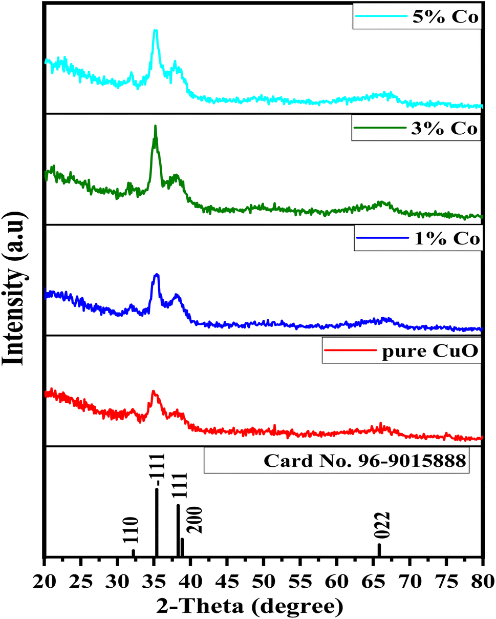
The properties of crystal structure and the phase purity of the photoelectrodes were examined by X-ray diffractometer instrument. X-ray patterns for all samples are depicted in Fig. 2, all peaks are accurately matched well to ICDD Card No. 96-9015888, confirming the monoclinic structure of all thin films with the space group C12/c1.28 The diffraction pattern also reveals that the CuO films exhibit a polycrystalline nature. The CuO films exhibited five prominent peaks at 2θ values of approximately 32.19°, 35.38°, 38.317°, 38.87°, and 67.357°, corresponding to the (110), (−111), (111), (200), and (022) planes, respectively. Additionally, no peaks or phases associated with Co were observed, indicating the successful growth of the CuO films without any phase change. Additionally, the incorporation of Co2+ at the Cu2+ site does not alter the structure of CuO film crystal. This is because the ionic radius of Co2+ (0.70 Å)26 is approximately close to that of Cu2+ (0.73 Å),27 allowing Co2+ ions to seamlessly integrate into Cu2+ sites within the CuO crystal lattice. Furthermore, there is no shift in the diffraction peaks, confirming that the Co ions are substituting Cu ions in the lattice without significantly changing the lattice parameters. This incorporation maintains the monoclinic structure of CuO, due to the similarity in the Co and Cu ionic radii, allowing Co to fit into the CuO lattice without causing major distortions.29,30 Based on the analysis of XRD peak intensities, the (−111) crystallographic plane shows higher intensity than other planes, indicating the primary diffraction peak and it is considered the main crystallographic orientation in CuO films. XRD peak intensity increases with the addition of Co content up to 3%, followed by a sudden decrease at 5% Co. This suggests that the crystallinity of the films improves with Co dopants up to 3%, this improvement may be due to the incorporation of Co2+ ions into the CuO matrix, which could enhance the arranging of the crystal structure. Co ions might stabilize the lattice structure, reducing defects or disorder at these doping levels.26,31 Moreover, increasing the Co contents more than this concentration led to poorer crystallinity. This could result from Co atoms exceeding the solubility limit, leading to lattice distortion, the formation of secondary phases, or an increase in structural defects32
 |
| | Fig. 2 XRD graph for Co doped CuO films and pure CuO. | |
Using the Debye–Scherrer equation, as shown in eqn (1)33,34 the prepared films' crystallite size (D) was determined.
| |
 | (1) |
In this equation,
β stands for full width at half maximum (FWHM),
λ for the X-ray beam's wavelength (∼1.54 Å),
θ for Bragg's angle, and
k for the shape factor (∼0.94).
Table 1 displays the structural characteristics that were determined for the (−111) crystallographic plane. Additionally,
eqn (2) was used to assess the dislocation density, and
eqn (3) was used to determine the micro-strain values.
35| |
 | (2) |
| |
 | (3) |
Table 1 Estimated parameters for all deposited photoelectrodes
| Parameter/sample |
Pure-CuO |
Co 1% |
Co 3% |
Co 5% |
| 2θ (°) |
35.21 |
35.27 |
35.197 |
35.23 |
| I (a.u.) |
216 |
240 |
393 |
329 |
| β (°) |
1.55 |
1.22 |
1.11 |
1.28 |
| D (nm) |
56.16 |
71.37 |
78.43 |
68.02 |
| δ (lines per m2) ×1014 |
3.17 |
1.96 |
1.63 |
2.16 |
| ε (lines−2 per m4) ×10−3 |
6.44 |
5.07 |
4.61 |
3.32 |
| Eg (ev) |
2.42 |
2.70 |
3.45 |
3.12 |
Based on Table 1, pure CuO thin films have an average crystallite size of 56.16 nm. The crystallite sizes for Co/CuO films were found to be 71.37 nm for 1% Co, 78.43 nm for 3% Co, and 68.02 nm for 5% Co. This shows how the crystallite size is irregularly affected by the dopant of Co into CuO. Moreover, the crystal formation is hindered by the migration of Co–O–Cu complexes to the surface, and this may be the reason of large crystallite sizes of Co doped CuO compared to pure CuO. Additionally, as mentioned, Co2+ ions have an ionic radius of approximately 0.70 Å, which can introduce defects, leading to lattice distortion due to the substitution of Co2+ ions. This results in a broadening of the XRD peaks. In general, doping transition metals can reduce crystal growth in metal oxides. The impurities formation on the surface of the crystal when Co2+ ions replace Cu2+ ions in the CuO lattice may be an explanation for the decrement in peak intensity.36,37
3.2. Morphology and elemental composition
The morphology of the surface for both CuO and Co/CuO films with varying dopant concentrations, fabricated via the SILAR method, was examined using field emission scanning electron microscopy (FE-SEM). Fig. 3 presents the SEM images for the pure and Co/CuO films, the images display a hierarchical “flower-like” morphology with nanoscale features resembling petals. This indicates a well-defined self-assembly process during film growth, which may arise due to the SILAR technique's ability to control layer-by-layer deposition.32 Moreover, all films exhibit a relatively uniform distribution of flower-like structures, suggesting good deposition control. The rough surface can enhance the surface area, which is beneficial for applications such as catalysis, sensing, and photoelectrochemical reactions. Cobalt doping often promotes the formation of more intricate morphologies, as Co ions can alter the nucleation and growth mechanisms during the SILAR process. The ionic radius of Co2+ is slightly smaller than Cu2+, and its incorporation into the CuO lattice can introduce lattice strain, influencing the film's morphology.38 Furthermore, the flower-like features become more prominent with Co doping, as cobalt ions act as nucleation centers, facilitating the formation of hierarchical structures. This can improve the surface area and active sites for applications. In addition, at higher doping levels, cobalt might hinder grain coalescence due to increased strain or defects, leading to smaller grains and more intricate morphologies. Moreover, the chemical composition of both pure CuO and Co/CuO films was determined by the energy-dispersive X-ray spectrometer (EDX). The EDX spectra for pure and 5% Co/CuO films are shown in Fig. 4a and b, respectively. The EDX analysis revealed that the Co/CuO thin films consist of cobalt (Co), oxygen (O2), and copper (Cu). The weight percentage (wt%) of cobalt in these electrodes ranges from 0.1 to 0.51 wt% as an average, depending on the amount of cobalt dopant used. These findings indicating the successful substitution of Co2+ ions for Cu2+ ions during the process of the thin film growth.
 |
| | Fig. 3 SEM images (a) pure CuO, (b) 1% Co/CuO, (c) 3% Co/CuO, and (d) 5% Co/CuO. | |
 |
| | Fig. 4 EDX spectra of (a) pure CuO and (b) 5% Co/CuO films. | |
3.3. Optical properties
UV-visible spectroscopy is an important and valuable instrument for investigating semiconductor materials' optical properties vai measuring their absorbance and transmittance in the visible and the UV region.32 The transmittance spectrum of undoped and Co/CuO photoelectrodes were evaluated using a PerkinElmer UV-visible spectrophotometer and are presented in Fig. 5(a). All electrodes exhibit low transmittance, about 15% in the visible regions, extending to approximately 650 nm. Additionally, all films achieve their highest transmittance in the near-infrared region, ranging from 800 to 1200 nm. However, adding Co dopants leads to a decline in transmission curves. The transmittance drops from 25% for undoped CuO to about 12% as a result of doping. This decrease may be due to photon absorbance scattering caused by defects in the crystal structure introduced by Co doping.17,39 The band gap and absorption coefficient are estimated from the transmittance spectra and Tauc's relation eqn (4):40where B is a proportionality constant, n = 2 for indirect and n = 1/2 for direct allowed transition optical bandgap semiconductors and α is known as the absorption coefficient that can be determined using the relation  where d and T are the thickness and the transmittance, respectively. In this study, the optical band gap values were determined by assuming an indirect allowed transition for CuO, which is consistent with previous reports on CuO-based thin films. Therefore, the value of n used in Tauc's relation was set to 2, corresponding to indirect transitions. The band gap energy (Eg) of each electrode is determined from the linear region in the (αhν)2 vs. hν graph by extrapolating at α = 0, as shown in Fig. 5(b). The pristine CuO film has an Eg of 2.42 eV which is higher than the bulk CuO (1.85), and it increases to about 3.4 eV with the addition of Co dopants. However, from the Tauc plot it observed that with increasing the doping level of Co dopants by more than 3%, the band gap is slightly decreased which can be attributed to the nanoparticles quantum confinement effect.32,41,42 Rehman et al.43 have also reported that intra-gap defects contribute to the reduction of the bandgap in CuO nanoparticles. Similarly, Ovchinnikov et al. have examined the impact of electronic defects in CuO, noting that intraband states form within the bandgap due to the existence of dopants or valence defects, such as oxygen vacancies and Cu1+ states. These defects are identified as key factors responsible for the bandgap narrowing in CuO nanoparticles.44
 |
| | Fig. 5 (a) Optical transmittance spectra of all films, (b) Taucs' plot of pure and Co/CuO thin films. | |
3.4. PEC measurements
The photoelectrochemical (PEC) properties of CuO and Co/CuO films were estimated by an electrochemical potentiostat, a xenon lamp of 400 W, and a homemade three-electrode system. LSV measurements were initially taken from −1 V to 1 V against the reference electrode (Ag/AgCl) that ranges from −0.4 V to 0.4 V vs. RHE, both in the dark and with illumination from the xenon lamp at around 100 mW cm−2. In Fig. 6(a), raising the voltage causes the photocurrent density to increase negatively, demonstrating that the produced films act as photocathodes and p-type semiconductors. Additionally, all samples exhibited negligible dark current. Under white light, the photocurrent density for the pure CuO photoelectrode achieved −0.5 mA cm−2 at −0.39 V via the RHE. Adding Co dopant boosted photocurrent density, peaking at −1.5 mA cm−2 at −0.39 V via the RHE, nearly triple that of the pure CuO photoelectrode.
 |
| | Fig. 6 PEC properties of pure CuO and Co/CuO photoelectrodes in 0.3 M Na2SO4 as an electrolyte. (a) Jph–V curves of all photocathodes, (b) ABPE% of all samples under white light illumination, (c) different values of IPCE% as a function of wavelengths for all films, and (d) the stability of the 3% Co/CuO photoelectrode under light illumination at an applied voltage of −0.4 V vs. RHE in a 0.3 M Na2SO4 electrolyte. | |
The PEC experiment was analyzed by coducting a potential between the counter and the working electrodes. This applied bias enhances the current flow from the working electrode to the counter electrode, influencing PEC performance. To account for this excess voltage, the applied bias photon-to-current conversion efficiency (ABPE%) is measured and estimated using eqn (5).30
| |
 | (5) |
1.23 V corresponds to the thermodynamic potential necessary for water splitting, while
Vbias represents the externally applied voltage. All calculations assume an approximately 100% faradaic efficiency.
Fig. 6(b) presents the ABPE% as a function of applied potential for all fabricated films under illumination (∼100 mW cm
−2). The data reveal that the 3% Co/CuO photoelectrode achieves the highest ABPE% compared to other photoelectrodes.
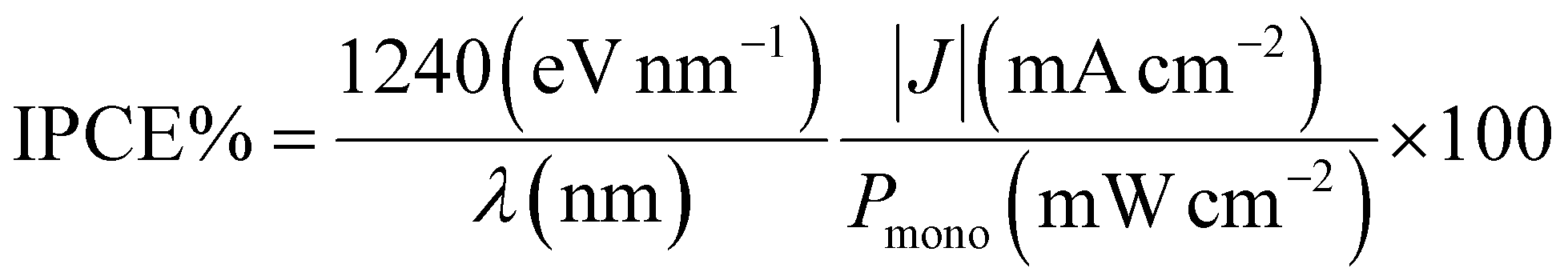
The incident photon-to-current conversion efficiency (IPCE%) measures the fraction of incident photons at a specific wavelength that successfully generates and contributes to the photocurrent.45 This metric is essential as it directly reflects the film's efficiency in converting absorbed photons into electrons. The IPCE% is calculated using eqn (6):46
| |
 | (6) |
Here,
J represents the photocurrent density at −1 V
versus Ag/AgCl,
λ denotes the wavelength of monochromatic illumination, and
P corresponds to the intensity of the monochromatic light. The constant 1240 results from the product of Planck's constant (
h) and the speed of light (
c). The IPCE% for the 3% Co/CuO photoelectrode is represented as a function of wavelength of monochromatic light in
Fig. 6(c). With bandgap of 3.4 eV, this photoelectrode primarily absorbs sunlight in the near-UV region (
λ ∼ 450 nm). As illustrated in
Fig. 6(c), the IPCE% spectrum shows a broad photoresponse extending across the visible range (400–650 nm), reaching a peak efficiency of 4.6% at 450 nm. The improvement in PEC performance upon Co doping can be attributed to multiple factors. Firstly, the introduction of Co
2+ ions creates localized energy states within the band gap, which facilitate improved light absorption and enhanced photogeneration of charge carriers. Secondly, Co doping can suppress charge recombination by acting as an electron trap, effectively prolonging the lifetime of photogenerated holes. Additionally, the presence of Co may increase the electrical conductivity of the film and improve the charge transport pathway toward the electrode/electrolyte interface. These combined effects result in higher photocurrent density and IPCE values compared to undoped CuO.
While calculating the ABPE and IPCE values, a faradaic efficiency of 100% was assumed for simplification, as commonly reported in related PEC studies using CuO-based photocathodes. However, we acknowledge that this assumption may not fully reflect the actual charge-to-product conversion efficiency in our system. Due to equipment and time constraints, direct experimental measurements of faradaic efficiency were not performed in this work. Nonetheless, previous reports on similar CuO-based systems under comparable operating conditions have demonstrated near-unity faradaic efficiencies, which justifies its use as a reasonable approximation in our analysis.30 We recognize this as a limitation of the current study and recommend future work to include direct quantification of evolved hydrogen and oxygen gases to verify the true faradaic efficiency and further validate the PEC performance. Furthermore, the stability of the photoelectrodes was evaluated under illumination at an applied voltage of −0.4 V vs. RHE in a 0.3 M Na2SO4 electrolyte, as shown in Fig. 6(d). All samples initially exhibited a rapid drop in photocurrent density to approximately 0.7 mA cm−2, which is most likely due to double-layer formation and photo-corrosion of the photoelectrode surface. Under continuous illumination and applied bias, chemical degradation processes may occur, impairing the surface and reducing the efficiency of charge generation and transport. After this initial drop, the current density stabilized at around 0.65 mA cm−2.
Notably, the 3% Co-doped CuO electrode demonstrated a more stable photocurrent over time compared to the undoped sample, indicating enhanced structural and chemical durability. This improved stability is likely due to the role of Co in passivating surface defects and suppressing photocorrosion, both of which are prevalent in pure CuO under operating conditions. Additionally, the enhanced crystallinity and modified grain structure resulting from Co doping may contribute to reduced degradation rates. To contextualize our findings, a comparative analysis with previously reported systems is presented in Table 3. While some studies report higher photocurrent densities than our achieved value of −1.5 mA cm−2, these often involve higher dopant concentrations, more complex fabrication procedures, or elevated processing temperatures. In contrast, our spatial SILAR-based approach offers a favorable balance of photoelectrochemical performance, ease of fabrication, and improved operational stability under illumination. These results highlight the practical advantages of low-level Co doping and flower-like morphology via SILAR, supporting its potential for scalable, low-cost PEC hydrogen production.
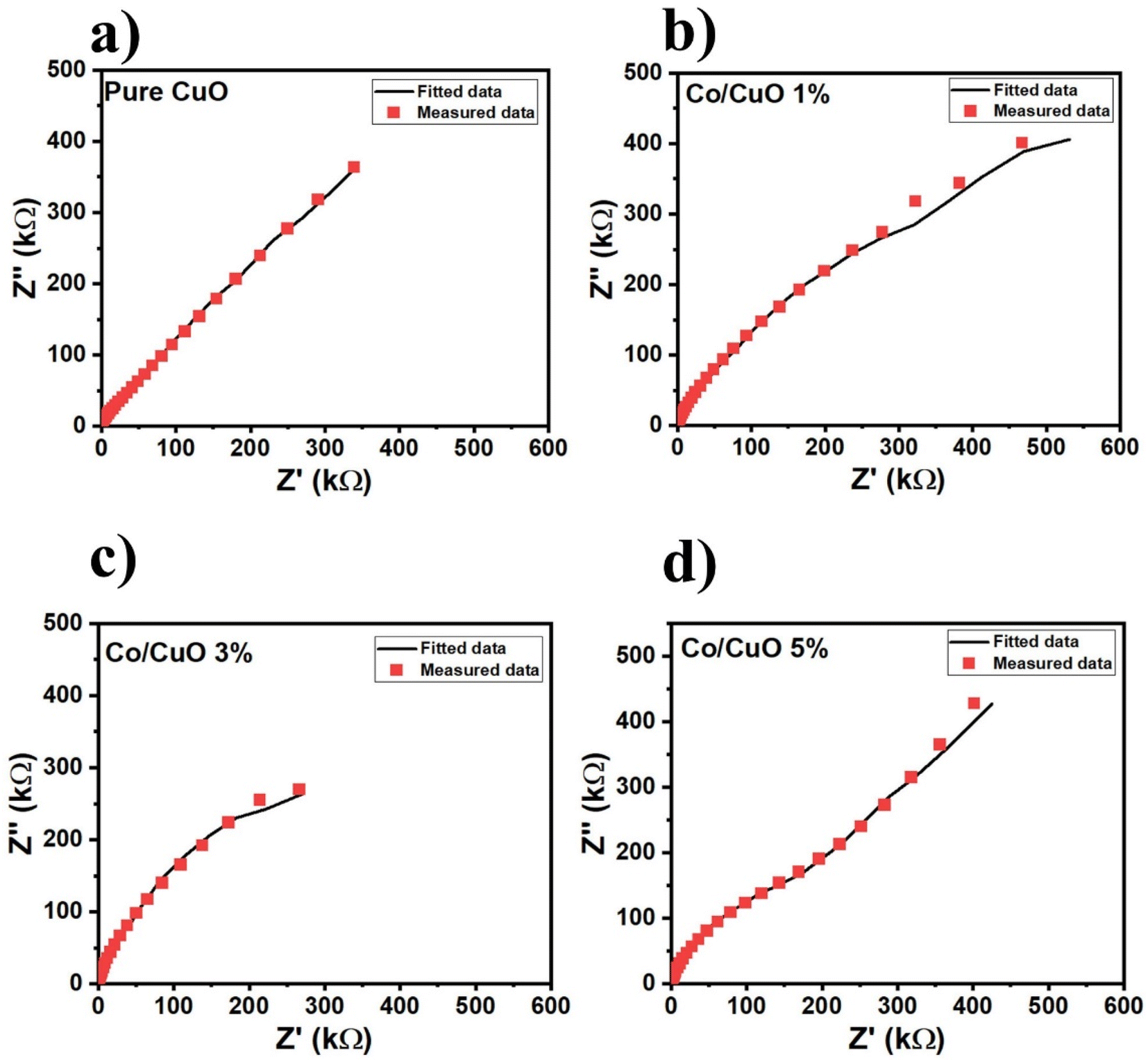
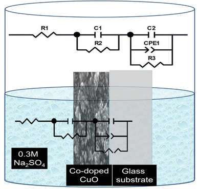
Electrochemical impedance spectroscopy (EIS) was measured to estimate the charge carrier dynamics at the photocathode/electrolyte interface. Measurements were performed at room temperature across a frequency range of 1 mHz to 1 MHz at 0 V vs. RHE and under white light. The EIS data were analyzed using Zview and ZsimpWin software to fit a simplified equivalent circuit. Fig. (7) displays the Nyquist plot of fitted data of all photoelectrodes dipped in a 0.3 M Na2SO4 electrolyte. The equivalent circuit, depicted in Fig. (8), consists of an electrolyte resistor (R1), which is evaluated from the high-frequency intercept in the Nyquist plot. This resistor represents charge transport through the electrolyte and it provides information about the amount of charges in the electrolyte. Furthermore, in our system as shown in Fig. (8), we have two layers, the electrolyte/thin-film layer, and the thin-film/substrate layer. Consequently, the simulated circuit includes two charge transfer resistors (R2 and R3), extracted from the semicircle diameter in the Nyquist plot, that reflect charge carrier migration across each layer. Additionally, a capacitor represents the double-layer capacitance, where higher capacitance values correspond to increased charge carrier and/or ion accumulation on the surface of the working electrode. Similarly, in the simulated circuit, we have two capacitors for each layer and a constant phase element (CPE) for the second interface between the thin film and the substrate. This CPE represents the nonideal capacitance behavior in our system, the value of n in CPE represents the ideality of capacitance behavior in the system i.e. 0 < n < 1 with n = 1 representing the ideal capacitive behavior. As shown in Table 2, the Co/CuO 3% photoelectrode exhibits a relatively low R1 value compared to other circuit components, indicating an efficient charge transportation process within the electrolyte. Moreover, increasing the Co contents led to an increase in the charge transfer resistance (R2) and consequently increase in the charge carrier recombination at the interface between the electrolyte and the electrode. Additionally, there are observed variations in the values of capacitance due to Co dopants, with higher capacitance value indicating more charge accumulation at the surface of the photoelectrode and this can affect the stability and charge transportation at the surface and the interface in the system. These results demonstrate that Co incorporation significantly improved the stability, light absorption, and charge carrier dynamics of CuO films.
 |
| | Fig. 7 EIS measurements at room temperature at 0 V vs. RHE and frequency ranges 1 mHz to 1 MHz and under white light illumination. | |
 |
| | Fig. 8 Schematic represents the equivalent circuit simulated by Zview and ZSimWin software. | |
Table 2 EIS results estimated using ZView and ZSimWin software
| |
Pure CuO |
Co/CuO 1% |
Co/CuO 3% |
Co/CuO 5% |
| R1 (Ω) |
33.95 |
36.43 |
24.04 |
38.29 |
| C1 (μF) |
1.4125 |
2.6636 |
2.1324 |
1.701 |
| R2 (kΩ) |
5.816 |
10.792 |
18.471 |
926.570 |
| C2 (μF) |
0.12972 |
0.1307 |
0.11871 |
0.046019 |
| R3 (MΩ) |
5.8326 |
1.223 |
0.695080 |
0.274180 |
| CPE-Y0 (S secn) |
2.3092 × 10⁻⁶ |
1.4611 × 10⁻⁶ |
1.2362 × 10⁻⁶ |
0.5085 × 10⁻⁶ |
| CPE-n |
0.54614 |
0.63889 |
0.83725 |
0.75413 |
4. Conclusion
This study provides a comprehensive discussion on the development of Co doped CuO-based photocathodes with promising performance in PEC water splitting. By exploring different Co dopants amounts, it was determined that these factors significantly influence the resulting photocurrent density and, consequently, the overall efficiency of PEC water splitting. Furthermore, an analysis of the essential parameters confirms that achieving a highly photoactive and photostable material requires an optimized surface area, controlled crystallinity, reduced charge carrier recombination, and a suitable electrolyte. The optical band gap energy were estimated as 2.42, 2.70, 3.45, and 3.12 eV for undoped CuO and Co/CuO 1%, Co/CuO 3%, and Co/CuO 5% respectively. In a photoelectrochemical cell, the CuO photocathode exhibited p-type semiconductor behavior. However, the Co-doped CuO photocathode demonstrated superior performance over pure CuO samples, achieving higher photocurrent density, improved anodic bias photon-to-current efficiency (ABPE%), and enhanced stability. In particular, the 3% Co-doped CuO thin film delivered photocurrent density of −1.5 mA cm−2 at −0.39 V vs. RHE about triple that of pure CuO photocathode, an incident photon-to-current conversion efficiency (IPCE%) of 4.6%, and outstanding electrochemical stability. These results highlight the potential of both undoped CuO and Co/CuO photocathodes as highly efficient materials for PEC water splitting, offering a favorable route for sustainable hydrogen generation. A benchmarking comparison (Table 3) further demonstrates that our Co-doped CuO photocathodes offer competitive PEC properties relative to previously reported systems. The novelty of this work lies in the use of low-level Co doping, spatial SILAR growth, and the resulting flower-like hierarchical morphology, which collectively contribute to enhanced PEC activity and operational durability. These findings provide a promising path forward for developing efficient and scalable CuO-based materials for solar hydrogen production.
Table 3 Photocurrent densities of the present work compared with selected prior studies using CuO-based photocathodes. The voltage listed in the table corresponds to the potential at which the respective photocurrent (J) was recorded. “RE” refers to the Ag/AgCl reference electrode, while “RHE” denotes the reversible hydrogen electrode
| Photoelctrode |
Testing conditions |
Photocurrent density |
Ref. |
| Co-doped CuO by SILAR |
0.3 M Na2SO4 pH = 7, 100 mW cm−2, -0.39 V vs. RHE |
J = −1.5 mA cm−2 |
This work |
| CuO photo-electrode with 10 at% Ni-doped seed layer on FTO substrate via the spin-coating |
1 M KOH, pH = 14, 300 W xenon lamp (100 mW cm−2), 0.7 V vs. RE |
J = 5 mA cm−2 |
12 |
| Cu2O and CuO by sol–gel technique |
0.1 M Na2SO4, pH = 5.84, 150 W xenon arc lamp (100 mW cm−2), 0.05 V vs. RHE |
J = −0.47 mA cm−2 |
20 |
| CuO films on FTO substrate by sol–gel technique |
0.1 M Na2SO4, pH = 6, 240 mW cm−2 visible-IR irradiation, 0 V vs. RHE |
J = −0.94 mA cm−2 |
22 |
| 1 at. in ms % Ni-doped CuO by chemical bath deposition |
1 M KOH, pH = 14, 300 W Xe-lamp (100 mW cm−2), −0.55 V vs. RE |
J = −1.75 mA cm−2 |
23 |
| Sm-doped CuO by RF-sputtering |
0.3 M Na2SO4 pH = 7, 100 mW cm−2, -0.385 V vs. RHE |
J = −4.66 mA cm−2 |
47 |
| Ti/p-CuO/n-Cu2O/Au by electrodeposition |
0.1 M sodium acetate, 100 W tungsten lamp (100 mW cm−2), 0 V vs. RE |
J = 310 μA cm−2 |
48 |
| 2% Ag-doped CuO by flame spray pyrolysis |
1 M KOH, pH = 14, AM 1.5 G solar simulator (100 mW cm−2), −0.7 V vs. RE |
J = −1.9 mA cm−2 |
49 |
| CuO/Cu2O by two-step electrodeposition method |
1 M Na2SO4, pH = 7, 150 W Xe-lamp, −0.7 V vs. RE |
J = −1.44 mA cm−2 |
50 |
Data availability
All data is available within the manuscript.
Conflicts of interest
There are no conflicts to declare.
Funding
This research work was funded by Umm Al-Qura University, Saudi Arabia for funding under grant number: 25UQU4250206GSSR03.
Acknowledgements
The authors extend their appreciation to Umm Al-Qura University, Saudi Arabia, for funding this research work through grant number 25UQU4250206GSSR03.
References
- P. Li, H. Zhang, Z. Zhang, Q. Hou, Z. Wen, X. Pan, X. Hao, A. Abudula and G. Guan, Biomass pyrolysis-gasification-hydrogen generation cycle system coupled with tar chemical looping reforming process, Int. J. Hydrogen Energy, 2024, 72, 367–379, DOI:10.1016/j.ijhydene.2024.05.263
 .
. - I. Hadjipaschalis, A. Poullikkas and V. Efthimiou, Overview of current and future energy storage technologies for electric power applications, Renewable Sustainable Energy Rev., 2009, 13, 1513–1522, DOI:10.1016/J.RSER.2008.09.028 .
- D. Huisingh, Z. Zhang, J. C. Moore, Q. Qiao and Q. Li, Recent advances in carbon emissions reduction: policies, technologies, monitoring, assessment and modeling, J. Cleaner Prod., 2015, 103, 1–12, DOI:10.1016/J.JCLEPRO.2015.04.098 .
- A. Ali and M. N. Shaikh, Recent developments in catalyst design for liquid organic hydrogen carriers: Bridging the gap to affordable hydrogen storage, Int. J. Hydrogen Energy, 2024, 78, 1–21, DOI:10.1016/j.ijhydene.2024.06.240 .
- M. Amende, A. Kaftan, P. Bachmann, R. Brehmer, P. Preuster and M. Koch, et al., Regeneration of LOHC dehydrogenation catalysts: In-situ IR spectroscopy on single crystals, model catalysts, and real catalysts from UHV to near ambient pressure, Appl. Surf. Sci., 2016, 360, 671–683, DOI:10.1016/J.APSUSC.2015.11.045 .
- J. Andersson and S. Grönkvist, Large-scale storage of hydrogen, Int. J. Hydrogen Energy, 2019, 44, 11901–11919, DOI:10.1016/j.ijhydene.2019.03.063 .
- W. Z. Tawfik, M. A. Hassan, M. A. Johar, S. Ryu and J. K. Lee, Highly conversion efficiency of solar water splitting over p-Cu2O/ZnO photocatalyst grown on a metallic substrate, J. Catal., 2019, 374, 276–283, DOI:10.1016/j.jcat.2019.04.045 .
- A. M. Ahmed, E. M. Abdalla and M. Shaban, Simple and Low-Cost Synthesis of Ba-Doped CuO Thin Films for Highly Efficient Solar Generation of Hydrogen, J. Phys. Chem. C, 2020, 124, 22347–22356, DOI:10.1021/ACS.JPCC.0C04760 .
- M. Hasan and N. Allam, Unbiased spontaneous solar hydrogen production using stable TiO2–CuO composite nanofiber photocatalysts, RSC Adv., 2018, 8, 37219–37228, 10.1039/c8ra06763e .
- V. Scuderi, G. Amiard, S. Boninelli, S. Scalese, M. Miritello, P. M. Sberna, G. Impellizzeri and V. Privitera, Photocatalytic activity of CuO and Cu2O nanowires, Mater. Sci. Semicond. Process., 2016, 42, 89–93, DOI:10.1016/j.mssp.2015.08.008 .
- S. Emin, F. F. Abdi, M. Fanetti, W. Peng, W. Smith, K. Sivula, B. Dam and M. Valant, A novel approach for the preparation of textured CuO thin films from electrodeposited CuCl and CuBr, J. Electroanal. Chem., 2014, 717–718, 243–249, DOI:10.1016/j.jelechem.2014.01.038 .
- J. Oh, H. Ryu, W. J. Lee and J. S. Bae, Improved photostability of a CuO photoelectrode with Ni-doped seed layer, Ceram. Int., 2018, 44, 89–95, DOI:10.1016/J.CERAMINT.2017.09.129 .
- D.-Y. Wang, M. Gong, H.-L. Chou, C.-J. Pan, H.-A. Chen and Y. Wu, et al., Highly Active and Stable Hybrid Catalyst of Cobalt-Doped FeS2 Nanosheets–Carbon Nanotubes for Hydrogen Evolution Reaction, J. Am. Chem. Soc., 2015, 137, 1587–1592, DOI:10.1021/ja511572q .
- A. Abdelmoneim, M. A. K. Elfayoumi, M. Sh Abdel-wahab, A. M. Al-Enizi, J. K. Lee and W. Z. Tawfik, Enhanced solar-driven photoelectrochemical water splitting using nanoflower Au/CuO/GaN hybrid photoanodes, RSC Adv., 2024, 14, 16846–16858, 10.1039/D4RA01931H .
- H. Xing, E. Lei, Z. Guo, D. Zhao and Z. Liu, Enhancement in the charge transport and photocorrosion stability of CuO photocathode: The synergistic effect of spatially separated dual-cocatalysts and p–n heterojunction, Chem. Eng. J., 2020, 394, 124907, DOI:10.1016/j.cej.2020.124907 .
- H. Xing, E. Lei, D. Zhao, X. Li, M. Ruan and Z. Liu, A high-efficiency and stable cupric oxide photocathode coupled with Al surface plasmon resonance and Al2O3 self-passivation, Chem. Commun., 2019, 55, 15093–15096, 10.1039/C9CC07978E .
- J. Uddin, M. Sharmin, M. N. Hasan and J. Podder, Influence of Ni doping on the morphological, structural, optical and electrical properties of CuO thin films deposited via a spray pyrolysis, Opt. Mater., 2021, 119, 111388, DOI:10.1016/J.OPTMAT.2021.111388 .
- S. Dolai, R. Dey, S. Das, S. Hussain, R. Bhar and A. K. Pal, Cupric oxide (CuO) thin films prepared by reactive d.c. magnetron sputtering technique for photovoltaic application, J. Alloys Compd., 2017, 724, 456–464, DOI:10.1016/J.JALLCOM.2017.07.061 .
- S. Al-Amri, M. Shahnawaze Ansari, S. Rafique, M. Aldhahri, S. Rahimuddin and A. Azam, et al., Ni Doped CuO Nanoparticles: Structural and Optical Characterizations, Curr. Nanosci., 2014, 11, 191–197, DOI:10.2174/1573413710666141024212856 .
- Y. Lim, C. Chua, C. Lee and D. Chi, Sol–gel deposited Cu2O and CuO thin films for photocatalytic water splitting, Phys. Chem. Chem. Phys., 2014, 16, 25928–25934, 10.1039/C4CP03241A .
- W. Z. Tawfik, Z. S. Khalifa, M. S. Abdel-Wahab and A. H. Hammad, Sputtered cobalt doped CuO nano-structured thin films for photoconductive sensors, J. Mater. Sci.: Mater. Electron., 2019, 30, 1275–1281, DOI:10.1007/s10854-018-0395-0 .
- J. Toupin, H. Strubb, S. Kressman, V. Artero, N. Krins and C. Laberty-Robert, CuO photoelectrodes synthesized by the sol–gel method for water splitting, J. Sol-Gel Sci. Technol., 2019, 89, 255–263, DOI:10.1007/S10971-018-4896-3 .
- J. w. Ha, J. Oh, H. Choi, H. Ryu, W. J. Lee and J. S. Bae, Photoelectrochemical properties of Ni-doped CuO nanorods grown using the modified chemical bath deposition method, J. Ind. Eng. Chem., 2018, 58, 38–44, DOI:10.1016/J.JIEC.2017.09.004 .
- M. Patel, R. Pati, P. Marathey, J. Kim, I. Mukhopadhyay and A. Ray, Highly Photoactive and Photo-Stable Spray Pyrolyzed Tenorite CuO Thin Films for Photoelectrochemical Energy Conversion, J. Electrochem. Soc., 2016, 163, H1195–H1203, DOI:10.1149/2.1081614JES/META .
- C. V. Niveditha, M. J. J. Fatima and S. Sindhu, Comprehensive Interfacial Study of Potentio-Dynamically Synthesized Copper Oxide Thin Films for Photoelectrochemical Applications, J. Electrochem. Soc., 2016, 163, H426–H433, DOI:10.1149/2.0971606JES/META .
- A. Sharma, R. K. Dutta, A. Roychowdhury, D. Das, A. Goyal and A. Kapoor, Cobalt doped CuO nanoparticles as a highly efficient heterogeneous catalyst for reduction of 4-nitrophenol to 4-aminophenol, Appl. Catal., A, 2017, 543, 257–265, DOI:10.1016/J.APCATA.2017.06.037 .
- B. P. Singh, M. Chaudhary, A. Kumar, A. K. Singh, Y. K. Gautam and S. Rani, et al., Effect of Co and Mn doping on the morphological, optical and magnetic properties of CuO nanostructures, Solid State Sci., 2020, 106, 106296, DOI:10.1016/J.SOLIDSTATESCIENCES.2020.106296 .
- N. J. Calos, J. S. Forrester and G. B. Schaffer, A Crystallographic Contribution to the Mechanism of a Mechanically Induced Solid State Reaction, J. Solid State Chem., 1996, 122, 273–280, DOI:10.1006/JSSC.1996.0113 .
- A. Maini and M. A. Shah, Investigation on physical properties of nanosized copper oxide (CuO) doped with cobalt (Co): A material for electronic device application, Int. J. Ceram. Eng. Sci., 2021, 3, 192–199, DOI:10.1002/CES2.10097 .
- A. M. Ibrahim, M. S. Abdel-wahab, M. A. K. Elfayoumi and W. Z. Tawfik, Highly efficient sputtered Ni-doped Cu2O photoelectrodes for solar hydrogen generation from water-splitting, Int. J. Hydrogen Energy, 2023, 48, 1863–1876, DOI:10.1016/J.IJHYDENE.2022.10.089 .
- D. Kamlaji Chavan, Synthesis and Structural Properties of Co Doped CUO Thin Films by Spray Pyrolysis, IOSR J. Appl. Phys., 2018, 10, 27–29, DOI:10.9790/4861-1004032729 .
- D. Warda, G. Noubeil and M. Kamel, Effect of Co-doping on Structural, Morphological, Optical and Electrical Properties of p-type CuO Films, J. Nano-Electron. Phys., 2023, 15, 06009, DOI:10.21272/jnep.15(6).06009 .
- S. Qutb, S. El-Dek, M. Hussien, M. Abdel-wahab and W. Z. Tawfik, Boosting photoelectrochemical water splitting performance via nanostructured Ag-CuO thin films, Phys. B, 2025, 696, 416672, DOI:10.1016/j.physb.2024.416672 .
- P. Scherrer, Bestimmung der Größe und der inneren Struktur von Kolloidteilchen mittels Röntgenstrahlen, in Chemische Technologie in Einzeldarstellungen, ed. K. Ein Lehrbuch, Springer, Berlin, Heidelberg, 1912, DOI:10.1007/978-3-662-33915-2_7 .
- K. Khot, S. Mali and N. Pawar, et al., Development of nanocoral-like Cd (SSe) thin films using an arrested precipitation technique and their application, New J. Chem., 2014, 38, 5964–5974, 10.1039/C4NJ01319K .
- D. Masekela, L. K. Kganyakgo, K. D. Modibane, T. L. Yusuf, S. A. Balogun and W. M. Seleka, et al., Green synthesis and enhanced photocatalytic performance of Co-Doped CuO nanoparticles for efficient degradation of synthetic dyes and water splitting, Results Chem., 2025, 13, 101971, DOI:10.1016/J.RECHEM.2024.101971 .
- M. Shaban, A. M. El Sayed, H. AlMohamadi, M. T. Khan and A. M. Ahmed, Effects of transition metals (Fe, Co) on the physical and photoelectrochemical hydrogen generation properties of copper oxide nanoparticulate films, Int. J. Hydrogen Energy, 2024, 56, 164–174, DOI:10.1016/J.IJHYDENE.2023.12.145 .
- W. Darenfad, N. Guermat and K. Mirouh, Effect of Co-doping on Structural, Morphological, Optical and Electrical Properties of p-type CuO Films, J. Nano-Electron. Phys., 2023, 15, 06009, DOI:10.21272/JNEP.15(6).06009 .
- H. Xing, E. Lei, Z. Guo, D. Zhao, X. Li and Z. Liu, Exposing the photocorrosion mechanism and control strategies of a CuO photocathode, Inorg. Chem. Front., 2019, 6, 2488–2499, 10.1039/C9QI00780F .
- O. Messaoudi, I. B. Assaker, M. Gannouni, A. Souissi, H. Makhlouf and A. Bardaoui, et al., Structural, morphological and electrical characteristics of electrodeposited Cu2O: Effect of deposition time, Appl. Surf. Sci., 2016, 366, 383–388, DOI:10.1016/J.APSUSC.2016.01.035 .
- S. P. Kamble and V. D. Mote, Structural, optical and magnetic properties of Co doped CuO nano-particles by sol-gel auto combustion technique, Solid State Sci., 2019, 95, 105936, DOI:10.1016/J.SOLIDSTATESCIENCES.2019.105936 .
- S. R. Qutb, W. Z. Tawfik, S. I. El-Dek, M. R. Hussein and M. S. Abdel-wahab, Superior photoelectrodes of nanostructured Mo-doped CuO thin film for green hydrogen generation from photoelectrochemical water-splitting, Int. J. Hydrogen Energy, 2024, 76, 190–201, DOI:10.1016/J.IJHYDENE.2024.03.200 .
- S. Rehman, A. Mumtaz and S. K. Hasanain, Size effects on the magnetic and optical properties of CuO nanoparticles, J. Nanopart. Res., 2011, 13, 2497–2507, DOI:10.1007/s11051-010-0143-8 .
- S. G. Ovchinnikov, B. A. Gizhevskiǐ, Y. P. Sukhorukov, A. E. Ermakov, M. A. Uǐmin and E. A. Kozlov, et al., Specific features of the electronic structure and optical spectra of nanoparticles with strong electron correlations, Phys. Solid State, 2007, 49, 1116–1120, DOI:10.1134/S1063783407060169/METRICS .
- A. Abdelmoneim, M. S. Abdel-Wahab, M. A. K. Elfayoumi, A. M. Ahmed, A. M. Ibrahim and H. Hamdy, et al., Enhancing the solar hydrogen generation performance of nickel-oxide nanostructured thin films doped with molybdenum, Phys. Scr., 2024, 99, 045906, DOI:10.1088/1402-4896/AD2C4A .
- F. Mohamed, M. Rabia and M. Shaban, Synthesis and characterization of biogenic iron oxides of different nanomorphologies from pomegranate peels for efficient solar hydrogen production, J. Mater. Res. Technol., 2020, 9, 4255–4271, DOI:10.1016/J.JMRT.2020.02.052 .
- M. S. Abdel-wahab, A. M. Ibrahim, A. A. Farghali and W. Z. Tawfik, Sputtered nanocrystalline samarium doped CuO photoelectrode for efficient photoelectrochemical water splitting, Mater. Today Commun., 2023, 37, 107122, DOI:10.1016/j.mtcomm.2023.107122 .
- R. P. Wijesundera, Fabrication of the CuO/Cu2O heterojunction using an electrodeposition technique for solar cell applications, Semicond. Sci. Technol., 2010, 25, 045015, DOI:10.1088/0268-1242/25/4/045015 .
- C. Y. Chiang, Y. Shin and S. Ehrman, Dopant effects on conductivity in copper oxide photoelectrochemical cells, Appl. Energy, 2016, 164, 1039–1042, DOI:10.1016/J.APENERGY.2015.01.116 .
- R. Borkar, R. Dahake, S. Rayalu and A. Bansiwal, Copper Oxide Nanograss for Efficient and Stable Photoelectrochemical Hydrogen Production by Water Splitting, J. Electron. Mater., 2018, 47, 1824–1831, DOI:10.1007/S11664-017-5966-Y .
|
| This journal is © The Royal Society of Chemistry 2025 |
Click here to see how this site uses Cookies. View our privacy policy here. 
 Open Access Article
 This Open Access Article is licensed under a Creative Commons Attribution-Non Commercial 3.0 Unported Licence
 a,
Ahmed Rida Galaly
a,
Ahmed Rida Galaly


 where d and T are the thickness and the transmittance, respectively. In this study, the optical band gap values were determined by assuming an indirect allowed transition for CuO, which is consistent with previous reports on CuO-based thin films. Therefore, the value of n used in Tauc's relation was set to 2, corresponding to indirect transitions. The band gap energy (Eg) of each electrode is determined from the linear region in the (αhν)2 vs. hν graph by extrapolating at α = 0, as shown in Fig. 5(b). The pristine CuO film has an Eg of 2.42 eV which is higher than the bulk CuO (1.85), and it increases to about 3.4 eV with the addition of Co dopants. However, from the Tauc plot it observed that with increasing the doping level of Co dopants by more than 3%, the band gap is slightly decreased which can be attributed to the nanoparticles quantum confinement effect.32,41,42 Rehman et al.43 have also reported that intra-gap defects contribute to the reduction of the bandgap in CuO nanoparticles. Similarly, Ovchinnikov et al. have examined the impact of electronic defects in CuO, noting that intraband states form within the bandgap due to the existence of dopants or valence defects, such as oxygen vacancies and Cu1+ states. These defects are identified as key factors responsible for the bandgap narrowing in CuO nanoparticles.44