
Recent progress of organic photonic synaptic transistors for artificial visual systems: structure configuration and innovative applications
Yiwen
Ren
a,
Lingjie
Sun
 *ab,
Yidi
Xie
a,
Shaosong
Gao
a,
Yuhan
Du
a,
Ming
Zhang
a,
Xianshuo
Wu
a,
Xiaoting
Zhu
a,
Fangxu
Yang
*a and
Wenping
Hu
a
*ab,
Yidi
Xie
a,
Shaosong
Gao
a,
Yuhan
Du
a,
Ming
Zhang
a,
Xianshuo
Wu
a,
Xiaoting
Zhu
a,
Fangxu
Yang
*a and
Wenping
Hu
a
aKey Laboratory of Organic Integrated Circuits, Ministry of Education & Tianjin Key Laboratory of Molecular Optoelectronic Sciences, Department of Chemistry, School of Science, Tianjin University, Tianjin 300072, China. E-mail: yangfangxu@tju.edu.cn; sunlingjie@tju.edu.cn
bKey Laboratory of Organic Integrated Circuits, Ministry of Education & Tianjin Key Laboratory of Molecular Optoelectronic Sciences, Department of Chemistry, Institute of Molecular Aggregation Science, Tianjin University, Tianjin 300072, China
First published on 28th May 2024
Abstract
Realizing an artificial visual system (AVS) integrating information perception, processing, and memory promotes the development of artificial intelligence technology. Organic photonic synaptic transistors (OPSTs) are promising candidates to mimic the human visual nervous system, as they combine the functions of light sensing and synaptic plasticity into one device. This article provides a comprehensive and systematic review of OPSTs used for AVSs. Firstly, the typical structures of OPSTs were introduced. These structures include a single organic semiconductor layer, bulk heterojunction, plane heterojunction, floating gate, and other novel structures. The functional materials, device performance, and characteristics, as well as the advantages and disadvantages of each device structure, were summarized. Following this, the innovative applications of OPSTs in AVSs were discussed, including image processing, visual adaptation, and motion detection. Finally, the main challenges and future developments in this field were considered.
 Lingjie Sun | Lingjie Sun received her PhD degree from the Department of Chemistry, School of Science, Tianjin University, in 2020 under the supervision of Prof. Wenping Hu. Then, she carried out postdoctoral research training at the Joint School of National University of Singapore and Tianjin University. In 2024, she is serving as an associate Professor at the Institute of Molecular Aggregation Science of Tianjin University. Her research interests are in the design, characterization, and optoelectronic properties of organic cocrystals. |
1. Introduction
Artificial visual systems (AVSs) are a cutting-edge field of scientific and technological development in the 21st century, almost ubiquitous in modern civilized life, covering a wide range of applications, including image classification, facial recognition, autonomous driving, security monitoring, robots, smart cities, etc.1–6 Traditional visual systems are typically composed of two physically separated units: an external camera unit for image perception and a processor unit for image memory and processing. Due to the need for a large amount of data conversion and transmission between physically separated light sensing units, memory units, and processing units, there are problems such as long response time and high energy consumption, which cannot meet the needs of artificial intelligence, big data, and Internet of Things (IoT) concepts. In contrast, the human visual system can quickly and efficiently identify target objects and extract useful information in complex environments with low energy consumption.7–13 Therefore, developing an AVS inspired by the human visual system with perception, processing, and memory functions is considered a promising solution.9,11,14,15AVSs generally need photosensitive synaptic devices, which can integrate sensing, computing, and memory functions into one device, such as phase change memory,16,17 memristors,18–20 field-effect transistors,21–23 and other optoelectronic devices. Compared to two-terminal devices, transistors have more signal modulation methods (light stimulation and gate voltage stimulation), higher control degrees of freedom (gate voltage regulation), higher fault tolerance, and higher signal-to-noise ratio.24–28 In addition, photonic synaptic transistors have the advantages of high efficiency, low power consumption, low crosstalk, and parallel processing.27–30 They are suitable for ultrafast neuromorphic computing and are considered one of the most promising unit devices for realizing AVSs. Recently, inorganic materials have achieved great success in the development of an AVS and promoted the development of this emerging field. Nonetheless, the integration of inorganic materials into flexible and biocompatible AVSs still presents challenges due to their rigidity and high processing costs. It is necessary to introduce organic materials to continue expanding this field's development. Due to significant advantages of diverse chemical structures, large-area solution processing, biocompatibility, good mechanical flexibility, and lightweight, organic semiconductor (OSC) materials are ideal candidate materials for biomimetic devices. Organic photonic synaptic transistors (OPSTs) based on OSC materials can not only achieve perception and memory of light signals, but also facilitate their application in the next generation of flexible, scalable, and skin-friendly biomimetic electronic products, opening up innovative application areas for artificial intelligence electronic devices.31–33
The core requirement of OPSTs is that the conductivity of the device can be controlled by light while maintaining memory, thus achieving behavior similar to human brain synaptic weight regulation. The most common working mechanism in OPSTs is to capture/de-capture charge carriers based on charge traps. The possible locations of charge traps in the structure include within the OSC layer, at the interface between the OSC and dielectric layers, and within the dielectric layer. This has driven the development of single OSC layer structures, heterojunction structures, floating gate structures, etc. for use in OPSTs. However, the current review lacks a summary of this section, which poses tremendous challenges for understanding and utilizing the charge-trapping mechanism. Therefore, it is necessary to conduct in-depth research on the charge trapping mechanism and develop effective introduction strategies to develop OPSTs with excellent conductivity regulation memory ability and multi-field collaborative regulation. In addition, the operational power consumption of OPSTs is one of the focuses of attention in this field, as the prominent feature of the human brain is that it only requires a small amount of energy to perform computational work. Reasonably designing the structure of OPSTs with power consumption close to or lower than that of a single synapse in the human brain remains a challenging task. Furthermore, wavelength sensing is one of the important functions of the human visual system, and simulating this function in OPSTs has attracted widespread attention from researchers. The single OSC can only respond to specific wavelengths, and introducing more functional materials into transistor structures to prepare OPSTs with a wide spectral response is a deliberate task. Last but not least, most of the current applications of OPST are limited to simulating some simple human behaviors and single pattern recognition tasks, such as MNIST pattern recognition, which resists their wide application in automatic driving, robot systems, etc. in the future.34–37 It is meaningful to exploit multifunctional and reconfigurable synaptic devices to achieve more emerging applications, such as bidirectional synapses, multi-level memory states, adjustable memory modes, and adaptability, through the design of device structures.38–42
In response to the issues mentioned above, a summary of recent research work has been made from the perspectives of the device structure and new applications (Fig. 1). In terms of the device structure, a single OSC layer structure is beneficial for mechanism research. We summarized some works on charge traps at the interface between OSCs and dielectric layers, as well as within the OSC layer, which laid the foundation for the rational construction of multi-field synergistic regulation of OPSTs. The introduction of functional materials (including perovskite materials, inorganic quantum dots, two-dimensional materials, pigment molecules, etc.) has formed bulk heterojunctions, plane heterojunctions, and floating gate structures with OSCs, for the development of more functions, including a wide spectral response, bidirectional synapses, adaptability, memory mode adjustability, etc. In addition, there are also some emerging structures (vertical structures, inverter devices, etc.) used to prepare low-power consumption OPST and broadband-responsive devices. Due to the rise of technologies such as facial recognition, biomimetic electronics, and autonomous driving, an increasing number of OPSTs can achieve efficient image processing, visual adaptation, and motion detection tasks. Finally, we put forward our thoughts and opinions on the challenges existing in the current development process of this field and guide the direction for future research, hoping to contribute to the development of this field.
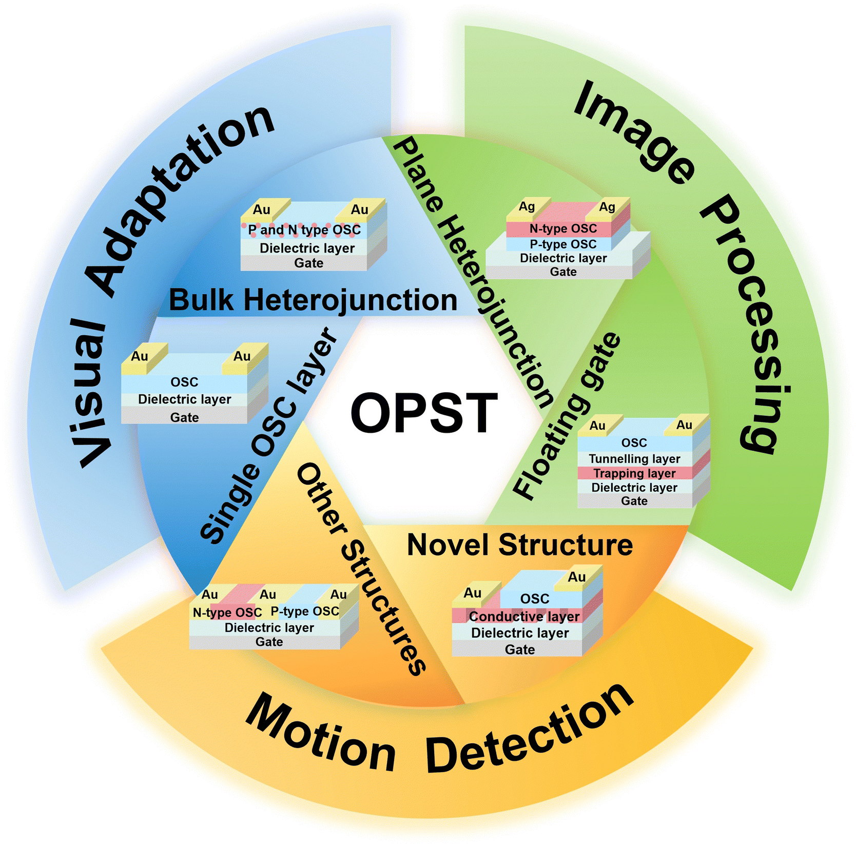 | ||
| Fig. 1 Overview of an organic photonic synaptic transistor for the artificial visual system from structure configuration and innovative applications. | ||
2. Structure configuration
2.1. Single organic semiconductor layer
Organic phototransistors are considered to be one of the viable basic units for the development of AVSs, with a three-terminal structure that can effectively modulate the carrier concentration and electric field distribution within the channel, allowing controllable modulation of the conductance magnitude. One of the most core materials is OSCs, which are materials with a conjugated π electron structure and semiconductor properties, including organic small molecule semiconductors and polymer semiconductors. Organic small molecule semiconductors have a relatively ordered solid structure formed by strong intermolecular interactions and can achieve relatively high mobility.43,44 Polymer semiconductors are mainly π-conjugated polymers that achieve interchain charge transport through π–π stacking, and their charge transport properties are comparable to those of amorphous silicon.45–47 Compared to inorganic materials, organic materials can tune the band gap of OSCs through appropriate molecular design to achieve tunable optoelectronic properties. In addition, organic materials have the advantages of low cost, solution processability, lightweight, and intrinsic flexibility, and are considered to be the most promising photosensitive materials with unique advantages in the field of developing flexible, wearable artificial visual devices. Here, we summarized organic small molecule semiconductors and organic polymer semiconductors for organic photonic synaptic transistors as shown in Fig. 2. The single OSC layer can not only absorb light within a certain wavelength range but can also serve as a charge transport layer to achieve the process of photoelectric conversion. The charge trapping inside the OSC or at the interface between the OSC and the dielectric layer is the most common working mechanism in photonic synaptic transistors, which enables the capture/removal of photo-generated carriers.48 As a result, the conductivity of the device can be controlled and memory retention can be achieved simultaneously, thus achieving a behavior similar to synaptic weight regulation in the human brain.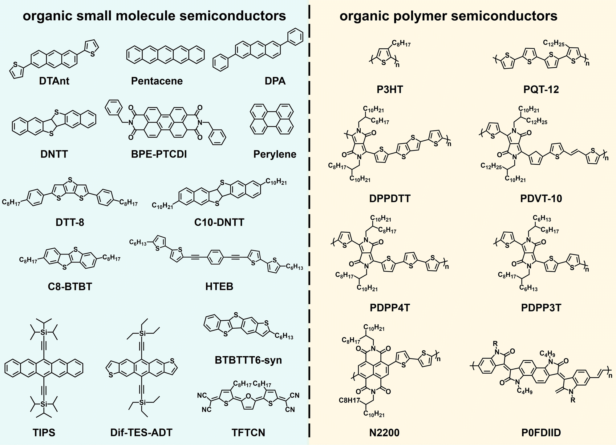 | ||
| Fig. 2 Summary of organic small molecule semiconductors and organic polymer semiconductors for organic photonic synaptic transistors. | ||
The charge transport and field effect properties of organic field effect transistors (OFETs) intensively depend on the interface quality and properties of the OSC and dielectric layers.49 SiO2 makes use of the dielectric layer in the majority of OFETs, but its surface contains a large number of hydroxyl groups, which are the traps in the process of carrier transport.50,51 The carriers are captured and the threshold voltage shifts, which seriously affects the performance of OFETs. However, they seem to be very advantageous in charge-trapping memory devices. In OPSTs, the mechanism of interface charge traps can be explained as follows: considering p-type OSCs for instance, under dark conditions, owing to the defects and traps at the interface capturing holes in OSCs, it is impossible to induce enough holes for charge transport at a small gate voltage. Therefore, the threshold voltage is relatively large. Under illumination, thanks to the generation of photogenerated carriers, some of the newly generated holes fill the defects of the interface, and the other holes participate in charge transport. At this time, it can be turned on without a larger gate voltage, the threshold voltage moves in the positive direction, and the source–drain current also reveals an increasing trend. Some OPSTs during the mechanism of charge traps at the interface are summarized below.
In 2019, Huang et al. first reported an OPST derived from two-dimensional molecular crystal (2DMC) C8-BTBT. By comparing the performance of the device with and without octadecyltrichlorosilane (OTS)-modified SiO2 surfaces, it was demonstrated that the synaptic behavior arises from the interfacial charge trapping effect. The synaptic behaviors including short-term plasticity (STP) and the learning ability of the device were successfully simulated.52 Then, Feng et al. reported that OSC single crystal DTAnt was employed in OPST. Because there is no modification in SiO2, it improved the charge trapping density, and the synaptic behavior stimulated by light was achieved.53 To further investigate the impact of different interfaces on synaptic performance, our group reported a controllable UV ultrasensitive neuromorphic visual sensor (Fig. 3a). The exciton binding energies at the interfaces of different dielectric layers (SiO2, SiO2/PMMA, SiO2/PS, and SiO2/PPO) and OSCs were obtained using the temperature-dependent photoluminescence (PL) spectra to be 127.8 meV, 13.2 meV, 16.0 meV, and 14.8 meV, respectively (Fig. 3b), with the exciton binding energies at the interfaces of SiO2 and OSC being much greater than those at the interfaces of other dielectric layers and OSC interfaces, indicating that the energy required to separate photogenerated excitons into free electrons and holes is larger.54 The theory is that charge trapping is the dominant factor in ultra-weak light detection and the synergistic effect of exciton binding energy and carrier mobility contributes to higher light intensity detection. Based on the ultra-weak light detection and interface charge trapping capabilities, photoelectric synaptic functions (Fig. 3c) with integrated sensing, non-volatile multilevel memory (Fig. 3d), and neuromorphic computation features are successfully realized.55 Similarly, OFETs with the interface effect between the polymer dielectric layer and OSC can also accomplish synaptic functions. Huang et al. discussed the influence of the molecular properties of the OSC and polymer dielectric layers on the two interface effect models of deep and shallow traps. The stronger the polarity of functional groups in polymer dielectric molecules, the shorter the side chain of the OSC, and the stronger the shallow trap interface effect. Short OSC side chains also bring about a deep trap interface effect. The shallow trap interface effect can be used for photoelectric detection, while the deep trap interface effect can be applied in photonic synaptic devices and photonic memory devices.56 Then, they selected PAN as the polymer dielectric layer. Since PAN has strong polar groups, it leads to a strong charge-trapping effect and complies with the function of a photonic synapse.57 In the same way, they implemented the detection of optical signals and simulated synaptic behavior by using the charge traps of the interface effect generated by the polar group –OH in PVA.58 These works revealed that the interface effect was a simple and widely applicable strategy to realize synaptic behavior, and the polymer dielectric layer laid a foundation for the realization of flexible synaptic devices, which is expected to provide new ideas for the design of future neuromorphic devices.
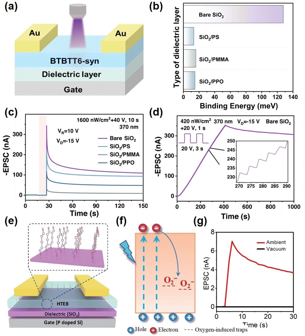 | ||
| Fig. 3 (a) The schematics of a neuromorphic vision organic sensor. (b) Binding energy with different interfaces of SiO2, SiO2/PS, SiO2/PMMA, and SiO2/PPO. (c) EPSC of the devices with different dielectric layers. (d) 100 consecutive UV presynaptic spikes. Reproduced with permission.53 Copyright 2023, Springer Nature. (e) Chemical Structure of HETB and sketch map of the HETB monolayer molecular crystal transistor. (f) The energy band diagram shows photo induced carriers from HTEB to oxygen induced levels. (g) The response to the same light stimulus under vacuum and ambient air conditions. Reproduced with permission.59 Copyright 2022, Tsinghua University Press. | ||
In addition to these, the existence of charge traps inside OSCs also enables the trapping/de-trapping of carriers. In 2019, Jie et al. proposed for the first time the theory that oxygen-induced deep-level traps in OSCs captured electrons, and the trapped electrons would be maintained in deep traps and underwent a slow release process after light illumination, resulting in the phenomenon of persistent photoconductivity (PPC) in OFETs.60 Based on this trapping mechanism, they subsequently prepared an all-solution-printed photonic synaptic transistor, introducing a strategy of the source Schottky barrier to regulate the carrier injection, which not only reduced the operating voltage and operating current but also obtained extraordinary synaptic ability and emulated synaptic plasticity with an ultra-low energy of 0.07 fJ.60 In 2021, our group grew C8-BTBT 2DMCs by the liquid substrate spatial confinement method, which overcame the interlayer shielding effect with excellent photogating and electrical gating effects to greatly reduce the off-state current of the transistor. The minimum off-state current was reduced by one to two orders of magnitude compared with bulk crystals or polycrystalline thin film structures, and the minimum current can be as low as 0.01 pA. The record-high photoresponse performances and tunable multilevel memory function were obtained based on C8-BTBT OPST. Besides, a series of characterization (Kelvin probe force microscopy and vacuum electrical testing) and comparison experiments demonstrated that the photogenerated electrons were trapped in oxygen-induced deep-level traps, exhibiting persistent photoconductivity.61 Identically, Huang et al. prepared HTEB monolayer molecular crystals for OPSTs using a drop-casting method to simulate biological synaptic functions (Fig. 3e) such as excitatory postsynaptic current (EPSC), paired-pulse facilitation (PPF) (PPF can be described as A2/A1 × 100%, where A1 and A2 are the EPSC values induced by two consecutive light pulses, respectively), short-term memory (STM) and long-term memory (LTM), demonstrating brain-like functions such as the dynamic learning–forgetting process and visual noise reduction, the synaptic behavior of which was also attributed to the oxygen-induced deep level traps (Fig. 3f and g).62 The single-layer device structure has advantages in revealing the mechanism of synaptic transistor devices, which lays the foundation for the development of multifunctional synaptic devices and the construction of multi-field coordinated regulation synaptic transistors by combining with dielectric layers or interfaces with excellent charge capture/de-capture capabilities.63
2.2. Bulk heterojunctions
Generally, OSCs and photoactive materials (such as perovskite quantum dots, pigment molecules, etc.) are mixed into bulk heterojunctions that are fabricated into hybrid films for photoelectric transistors. The preparation process of the bulk heterojunction is simpler, and the hybrid layer simplifies the device structure. At the same time, it increases the contact area between OSCs and the photoactive materials, directly exposing the photoactive materials to light, reducing carrier injection time, and ensuring efficient charge separation. In addition, the photoactive materials are encapsulated by hydrophobic OSCs, which further improves the stability of the photoactive materials.In 2019, Huang et al. demonstrated OPSTs based on solution preparation of inorganic halide perovskite (CsPbBr3) quantum dots (QDs) and organic polymer semiconductor PQT-12 hybrid thin films. The combination of OSCs and perovskite materials not only improves charge separation efficiency but also delays the attenuation of photocurrent, achieving high photoresponse performance and effective photonic synaptic function.64 In the same way, they mixed organic polymer semiconductors DPPDTT with high mobility and CsPbBr3 QDs with high photosensitivity to prepare devices that exhibited obvious synaptic behavior at ultra-low operating voltages of −0.0005 V. There was a large potential barrier between the valence band of perovskite QDs and the HOMO level of OSCs, which hindered the process of holes returning to perovskite QDs and further enhanced the synaptic performance of the device.65 In addition, they also prepared the same thin film on an environmentally friendly ion conductive cellulose nanopaper solid dielectric layer, and there was no distinct synaptic performance degradation when the radius of the synaptic device was curved to 1 mm (Fig. 4a–c).66 The logical function of OPST was realized by a synergistic modulation of photonic and electric operations. In 2021, Chi Ching Kuo et al. used the A-site substitution method to replace the original cesium (Cs+) with formamidinium (FA+), and the photo-physical properties of three different cations (FAPbBr3, FA0.5Cs0.5PbBr3, and CsPbBr3) were investigated. It was found that FAPbBr3 QDs had the deepest valence band and the longest exciton lifetime. P3HT/FAPbBr3 QD OPST was prepared, and ultrafast photoresponse time and a switch current ratio of 2.2 times under 1 ms of light stimulation were obtained.67 Moreover, the energy consumption of a single event is only 3 × 10⁻¹⁷ J. (Epc = Vd × Ipeak × t, where Vd, Ipeak, and t are the operating voltage, the corresponding EPSC peak value, and the light pulse duration, respectively.) Apart from these 0D perovskite QDs, perovskite nanoplates with 2D structures have advantages such as higher carrier mobility and larger absorption area, which are used to construct hybrid bulk heterojunction phototransistors. In 2023, Huang et al. developed CsPbBr3 nanoplates and P3HT mixed organic/inorganic heterojunction OPST. The efficient charge separation resulted in a single synaptic event energy consumption of only 0.053 fJ for this device. CsPbBr3 nanoplates and P3HT had complementary absorption ranges, enabling sensing operations for different wavelengths. Through the regulation of the wavelength of the light and gate voltage, the rapid switching between potentiation and depression synaptic behavior can be achieved, and based on this, the escape behavior of fruit flies toward food under red and blue light had been successfully simulated.68
 | ||
| Fig. 4 (a) Organic optoelectronic synaptic transistor based on CsPbBr3 QDs and the ICCN, and a photograph of a highly flexible optoelectronic synaptic transistor array. (b) The transition of STP to LTP is triggered by increasing the intensity of photonic pulses. (c) ΔEPSC induced by the photonic pulses with different wavelengths ranging from 400 to 650 nm at a fixed light intensity. Reproduced with permission.64 Copyright 2022, Elsevier Ltd. (d) The device structure of the OSC-Cl-HABI transistor and the schematic of the interactions between the external air and the DPP-DTT/Cl-HABI hybrid film. (e) The EPSC behaviors were simulated in the device under various humidity conditions. (f) The EPSC behaviors as a function of storage days under air conditions. Reproduced with permission.69 Copyright 2023, Wiley-VCH. (g) Schematic illustration and operating mechanism of the high-temperature synaptic phototransistors based on the DPPDTT/MI, and chemical structures of DPPDTT and MI. (h) Temperature-dependent EPSC results triggered by five consecutive presynaptic light pulses. (i) Effect of the operating temperature on PPF behavior. Reproduced with permission.70 Copyright 2023, Wiley-VCH. | ||
Additionally, natural pigment molecules also exhibit good light absorption. Inspired by plant photosynthesis, Huang et al. prepared a multifunctional OPST by blending natural chlorophyll and organic polymer semiconductor PDPP4T. The device exhibited excellent photoresponse values, including P = 2.7 × 10⁶, R = 2 × 10⁶ A W−1, and D* = 6 × 10¹⁵ Jones, resulting in a minimum operating voltage and power consumption of 10−5 V and 0.25 fJ, respectively. The conversion of the photodetector and photonic synaptic functions was achieved by adjusting the positive or negative gate voltage.71 In addition, the device has good mechanical flexibility and air stability. Subsequently, they also prepared this hybrid film on the dielectric layer of wood-derived cellulose nanopaper, revealing multifunctional synaptic behavior and excellent mechanical flexibility. Even when the bending radius of the flexible device was reduced to 1 mm, there was no apparent degradation of the synaptic performance.72 Besides, Huang et al. also applied a mixture of environmentally friendly natural pigment carotene and organic polymer semiconductor PDPP4T to synaptic transistors, realizing an ultra-low power consumption of 3.4 × 10⁻¹⁸ J. These investigations provide new guidance for the development of flexible organic neuromorphic visual systems based on environmentally friendly natural materials.73
To meet various functional requirements, such as broadening the light absorption range, improving charge separation efficiency, and providing charge traps, functional organic materials have been introduced into OPST. PCBM, the photosensitive and charge-trapping material, has been widely employed in various optoelectronic devices. Chen et al. created a p/n heterojunction OPST using PDVT-10 as the p-type OSC and PCBM as the n-type OSC. The combination of the two made the device indicate different synaptic properties at different wavelengths.69 Furthermore, Di et al. designed two complementary bulk heterojunctions to achieve photo-triggered active visual adaptation. The upper heterojunction PCBM/PDPP3T facilitates transient photoresponse behavior by photovoltaic effect-induced photoexcitation. Meanwhile, electron trapping at the interface of the lower heterojunction PCBM/P3HT and PVA resulted in a gradual decrease in gate voltage in the conductive channel. Upon light irradiation, light excitation occurred simultaneously in both heterojunctions, which was similar to the transient response of photoelectric transistors, and the subsequent electron trapping in the dielectric layer contributed to the dynamic shielding of the gate field, thus allowing the photoactive adaptation behavior in one device.70 More meaningfully, Huang et al. reported an OPST composed of a mixture of organic polymer semiconductor (DPPDTT) and photoinitiator molecules (Cl-HABI) (Fig. 4d).74 It demonstrated synaptic behavior, including EPSC, PPF, and learning and forgetting behavior, at varying humidity and oxygen concentrations, such as vacuum, dry, and humid environments (Fig. 4e and f), which was attributed to the charge trapping effect of photoinitiators that generated free radicals under light stimulation. Furthermore, OPST exhibited exceptional detection capability in the ultraviolet B region. Impressively, Huang et al. proposed a facile strategy of combining organic polymer semiconductors (DPPDTT) and the insulating matrix (MI) by high-temperature OPSTs with high glass-transition temperature (Fig. 4g), which addressed the issue of declining photoresponse performance in high-temperature environments. The interpenetrating network structure of DPPDTT and MI enabled them to maintain stable charge transport performance even under high-temperature operation. Additionally, the polar functional groups in MI provided charge traps, which enhanced photosensitivity and generated light-modulated memory behavior, achieving synaptic characteristics such as EPSC, PPF, and LTP/LTD in a wide operating temperature range from room temperature to 200 °C (Fig. 4h and i).75 These works demonstrate the potential of OPST based on organic materials, which will provide feasible solutions for future applications of neuromorphic visual systems and biomimetic robots in extreme environments.
A bulk heterojunction simplifies the device structure, reduces the complexity of device preparation, and can better absorb photon energy when directly exposed to light. Its light absorption efficiency should be higher than that of the floating gate structure and planar heterojunction structure under the same conditions. However, a bulk heterojunction also has its problems, such as whether OSCs and photoactive materials can be fully dissolved in the same solvent, whether photoactive materials can be evenly distributed in OSCs, whether photoactive materials will affect the nucleation and growth process of OSCs, the large off-state current of the device and so on.
2.3. Sandwich/multilayer heterojunction
Currently, the main mechanism of OPSTs is charge trapping, which commonly occurs within the OSC, at the interface between the OSC and the dielectric layer, or through charge traps introduced within the dielectric layer. The first two types of charge traps primarily result from unintentional but inevitable traps introduced during device fabrication, such as oxygen-induced deep-level traps inside OSCs, and polar functional groups at the interface of the OSC and the dielectric layer. However, the introduction of charge traps in the dielectric layer is designed to capture and de-capture both charge carriers and photo-generated charge carriers, which lays the foundation for constructing synaptic transistor devices with multi-field (electric field and light field) coordinated regulation. In recent years, various materials, for instance, perovskite materials, inorganic QDs, metal oxides, metal complexes, 2D polymers, and 2D materials, and OSCs form plane heterojunction structures or floating-gate structures. They respectively play a role in promoting charge separation and charge traps in plane heterojunction structures or floating gate structures. The introduction will then be divided into planar heterojunction structures and floating gate structures. | ||
| Fig. 5 Three types of heterojunctions are classified according to bandgap alignment. Type I: straddling gap; type II: staggered gap; and type III: broken gap. | ||
Organic–inorganic hybrid heterojunctions formed by OSCs and perovskite materials are widely used in OPST because they have superior properties of high optical absorption efficiency, low exciton binding energy, long exciton lifetime, high charge separation efficiency, wide spectral absorption, tunable band gap, and easy dispersion in solvents, and are widely employed in OPSTs.77–79 In contrast to OPSTs based on a single OSC, the introduction of perovskite materials provides extended functionality for OPSTs. For example, the high light absorption efficiency and charge separation efficiency of perovskite materials improve the photoresponse performance of devices. In 2021, Huang et al. constructed an OPST based on TIPS/CsPbBr3 hybrid film. The CsPbBr3 film had an island-like structure, effectively reducing hysteresis and achieving a specific detectivity of up to 2 × 10¹⁵ Jones. As a result of the outstanding detectivity of OPST, the apparent synaptic function of the device was attained by the stimulation of the light with a power of 1.6 nW at a low operating voltage of −1 V. Due to wide spectral absorption, broad-spectrum response devices can be constructed.80 To meet the requirement of a neuromorphic visual system, the appropriate band structure is designed to form heterojunctions between OSCs and perovskite materials. A 2D perovskite/organic heterojunction (PEA2SnI4/Y6) bipolar OPST was constructed through a solution method. The OPST exhibited high responsivity to visible light (104 A W−1) and near-infrared light (200 A W−1), inhibitory synaptic behavior under three visible light stimulation, red, green, and blue, and excitatory synaptic behavior under near-infrared light stimulation was demonstrated, which was applied to distinguish different colors of light.81 Besides, they proposed a tuned polymer/perovskite heterojunction interface defect strategy, which significantly improved the ability of charge trapping and de-trapping, and enhanced the separation and injection process of photo-generated carriers. The prepared OPST with a quick response speed of less than 35 ms perfectly mimicked the human visual synaptic behavior.82 There are many reports on fabricating advanced OPSTs based on OSC/perovskite material heterojunctions by low-cost solution processes; however, the preparation of a high-density perovskite/OSC heterojunction array remains a long-lasting challenge. In 2024, Huang et al. prepared perovskite QD/OSC micropatterning arrays with an effective cross-linking microlithography technique (Fig. 6a–c). The array presented minor device-to-device variation, high density (6500 device cm−2), and high yield (≈100%). The heterojunction neuromorphic photosensor arrays exhibited impressive performance with a photosensitivity of 3.2 × 10⁷, a responsivity of 1.92 × 10⁴ A W−1, high specific detectivity (1014 Jones), and low energy consumption (27.9 aJ) in a synaptic event.28
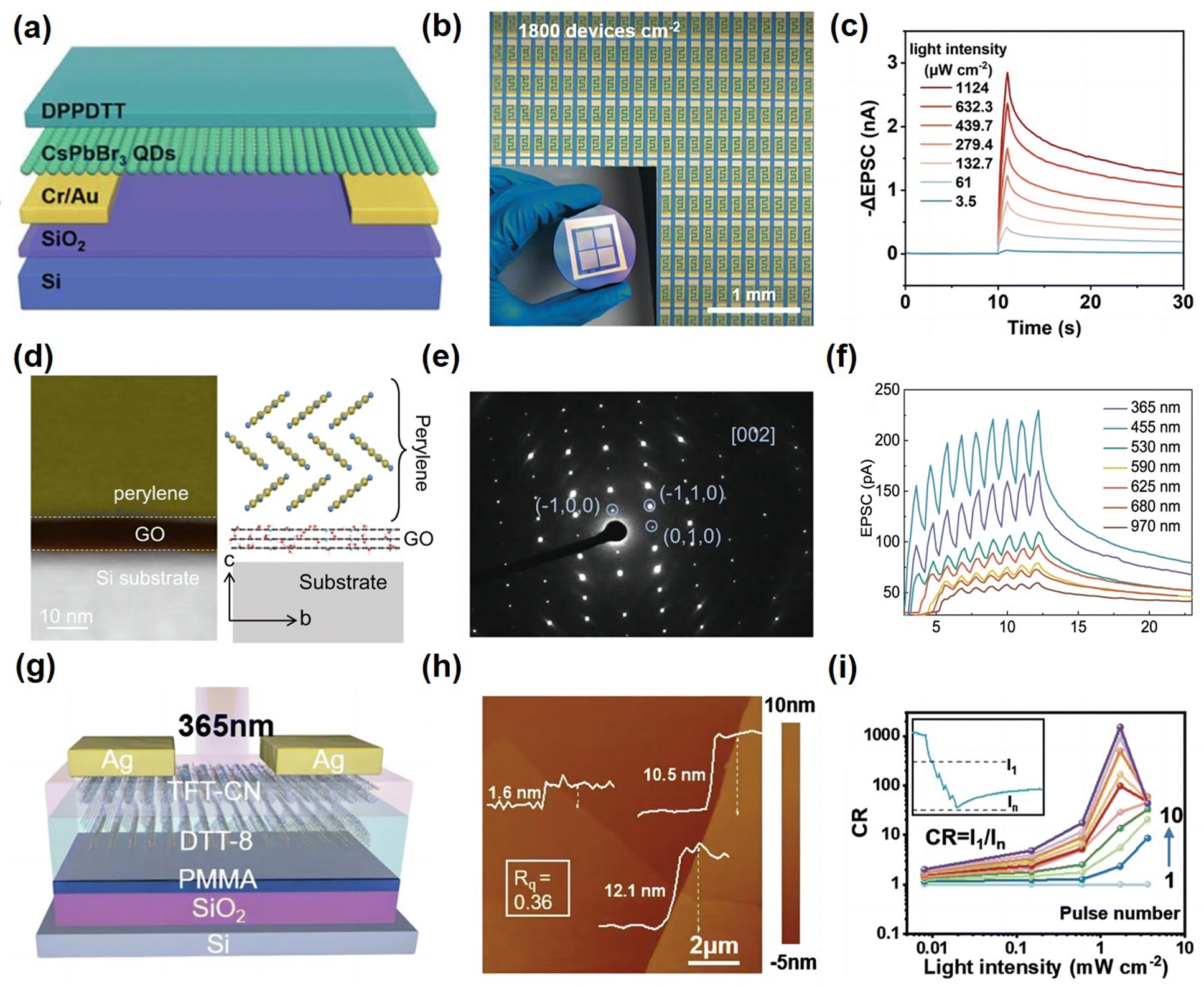 | ||
| Fig. 6 (a) Schematic diagram of the CsPbBr3 QD/DPPDTT PHJ-based OPT array. (b) Optical image of the CsPbBr3 QD/DPPDTT PHJ-based OPT array with a density of 1800 devices per cm2 (inset: the macroscopic optical image of the phototransistor array). (c) EPSC behaviors at various light intensities. Reproduced with permission.27 Copyright 2024, Wiley-VCH. (d) Schematic diagram of the device structure based on 2D molecular crystal heterojunctions. (e) AFM image of the 2DMC heterojunction; the inset images indicate the thicknesses of DTT-8, TFT-CN, and their combination. (f) Contrast ratio of IPSC from 1 to 10 light pulses at different light intensities. Reproduced with permission.83 Copyright 2022, Springer Nature. (g) Cross-section STEM image of the bilayer perylene/GO structure on a silicon holder and ordered molecular arrangement of the perylene crystal viewed from the b axis of the lattice and GO layer; yellow, carbon atom; blue, hydrogen atom. (h) SAED image of the perylene crystal. (i) EPSCs in response to nine successive light pulses under UV, visible and infrared light sources. Reproduced with permission.29 Copyright 2023, Wiley-VCH. | ||
OSCs have relatively large bandgaps and almost no infrared absorption, and it is difficult to separate excitons in them, which limits the progress of OPST responses in the infrared light range. Colloidal quantum dot materials (such as PbS QD, CuInSe2 QD, and CdSe QD) have narrow band gaps, high infrared absorption efficiency, and good stability. The relatively high mobility of OSCs can be used as a channel layer in OPSTs. Inorganic QD materials, as photosensitive materials, can not only enhance the absorption of infrared light and improve charge separation efficiency but also capture and de-capture photo-generated carriers due to the presence of defects. In 2023, Guo et al. prepared a short-wave infrared OPST with a PDPP-DTT/PbS QD heterojunction structure. The solvent-resistant PDPP-DTT was employed as the channel layer and spin-coated PbS QD with high infrared absorption efficiency above it, which promoted the carrier separation and introduced the interface defects to adjust the concentration of carriers in the channel by triggering the capture and release of electrons under illumination, achieving adaptive synaptic behavior in a white light environment.84
The above two inorganic materials are usually prepared by the spin-coating method and then combined with OSCs to form heterojunction structures. Besides, two-dimensional (2D) materials, such as graphene, MoS2, and OSC form heterojunction structures, which play a crucial role in constructing multifunctional, broadband, low energy consumption, and high-performance artificial visual devices due to their unique optical and electrical properties. Recently, graphene/organic heterojunction phototransistors have shown novel optoelectronic phenomena. For example, in 2022, Wang et al. achieved bidirectional photoresponse behavior by adjusting the gate voltage to change the position of the graphene Fermi level. The implementation of this behavior provides significant technical support for image sensing and convolutional processing in artificial vision. In addition, OPSTs based on inorganic/OSC heterojunctions exhibit unique advantages in weak light detection and low-energy synaptic devices due to their excellent photosensitive properties.83 In 2023, Huang et al. proposed a heterojunction OPST based on inorganic semiconductors (MoS2)/OSC (DNTT). The unique band structure of the heterojunction allowed the device to exhibit significant synaptic response characteristics even at ultra-weak light intensity (40 nW cm−2). At an operating voltage of 0.001 V, the energy consumption per synapse event is as low as 0.4 fJ.85 The successful implementation of this work provided a feasible approach for the development of inorganic/organic heterojunction OPSTs in the field of low energy consumption and ultra-sensitive multifunctional neuromorphic computing. This layer-by-layer stacking method for preparing organic–inorganic hybrid heterojunctions can cause problems such as the introduction of impurities during the preparation process, complex preparation techniques, and low transfer success rates. Hence, Huang et al. developed a method for interfacial coassembly of heterobilayer films of perylene and graphene oxide (GO) precursors, obtaining a uniform bilayer structure of single-crystal perylene and well-stacked GO that spans centimeters in size (Fig. 6d–f). The device had an ultra-high specific detectivity (3.1 × 10¹³ Jones), ultra-low power consumption (10−9 W), and excellent PPF index (214%).86 The development of controllable heterojunction growth and van der Waals non-destructive assembly technology still face significant challenges, which are crucial for the development of high-density artificial visual devices.
Apart from the inorganic photosensitive materials mentioned above, various functional organic photosensitive materials have also been widely applied in OPSTs. Ling et al. introduced the UV light absorption material (TFB) and constructed an OPST based on TFB/pentacene heterojunctions, which exhibited a unique UV response without other RGB interference. The current of the device increased as the duration and intensity of light exposure, demonstrating the synaptic characteristics of STM and LTM at different stages of UV radiation, and simulated the process of retinal damage under UV light.87 2D polymers and 2D metal–organic frameworks with fixed microporous structures, designable skeleton structures, and adjustable band structures are considered excellent photosensitive materials and charge-trapping materials. They not only provide outstanding photosensitive properties but also enhance charge capture and de-capture capabilities. In 2021, Huang et al. reported for the first time an OPST based on 2D polymers. The device not only achieved ordinary synaptic functions but also exhibited spectral-dependent synaptic behavior. At an operating voltage of 0.1 V, the energy consumption per synapse event was only 0.29 pJ, as a result of the high photosensitivity of 2D polymers and efficient charge separation of the heterojunction structure between 2D polymers and OSCs.88 They also explored the application potential of the OPST based on 2D MOFs. Through the regulation of the source–drain voltage, the band arrangement was changed to attain the variation of the magnitude of the light stimulus response current.89 Moreover, photochromic molecules have been studied for many years and have been applied in optical switching devices and multilevel nonvolatile memory devices. Due to their advantages of high photosensitivity, stability, and an adjustable energy level, they are considered to be the best candidates for multifunctional devices. Huang et al. introduced DAE molecules into OPSTs to achieve the goal of integrating photo response and photo memory in one device. The conversion of different functions was realized by adjusting the wavelength of the irradiated light. It showed positive photo response under visible light and negative photo memory under UV light, which was due to the change of the DAE molecular structure and energy level under UV and visible light irradiation.90 Similarly, the efficient charge separation and interesting band structure of organic p/n heterojunctions have special advantages in constructing multifunctional and ultra-sensitive OPSTs. In 2023, our group reported a method for preparing 2DMC heterojunctions of DTT-8 and TFTCN through layer-by-layer stacking (Fig. 6g and h). Due to the ultra-thin molecular thickness, excitons effectively separated and diffused in the 2D heterojunction, achieving ultra-high contrast (1.53 × 10³) and bidirectional synaptic behavior (Fig. 6i).30
In conclusion, OPSTs based on planar heterojunctions can play a role in the respective advantages of OSCs and photoactive materials to achieve low-voltage and low-power operation. Photoactive materials with different functions are introduced into heterojunctions. Because of their special photophysical properties and energy level structure, they play different roles, which lay a foundation for the multi-functional application and integration of devices.91
The significant requirement of OPSTs is that the conductivity of the channel can be controlled and memory retention can be achieved simultaneously, thereby achieving a behavior similar to synaptic weight regulation in the human brain, which usually requires the design of artificially designed charge traps. In 2021, Cheolmin Park et al. designed an OPST by area-density-tunable perovskite (MAPbBr3) nano-cone templated in a self-assemble block copolymer (Fig. 7a–c).93 Due to the Lewis acid–base interaction between perovskite and block copolymers, defect and size-controllable perovskite nanocrystals only coordinate within a local region of the block copolymer. Subsequently, a floating gate OPST with pentacene as the active layer was constructed by spin-coating polymer PS above. The gate field-dependent charge trapping and de-trapping behavior and synaptic behavior under both light and electrical stimulation were achieved owing to perovskite nanocrystals. A change of the density of perovskite nanocrystals in different regions through off-centered spin coating was attained (Fig. 7b), resulting in different charge trapping abilities at different positions, achieving position-dependent multifunctional synaptic behavior (Fig. 7c) and successfully simulating the retina with area-dependent photoreceptor cones. In 2023, Yi et al. blended CsPbBr3 perovskite QDs with PMMA to form an OPST with a floating gate structure, in which the perovskite QDs played a role in charge traps. By adjusting the gate voltage, excitatory and inhibitory synaptic behavior was achieved under light stimulation.94 These works provide us with new ideas for the rational design of charge traps.
 | ||
| Fig. 7 (a) Artificial photo reception system with a photoreceptive floating gate of perovskite NCs and an array of perovskite NCs templated in the BCP nanostructure. (b) The photograph of the off-centered BCP/MAPbBr3 film with the corresponding thickness gradient and the AFM height image was captured from the three regions of the film. (c) The photograph of 10 arrays of AIPS devices developed with an off-centered film. PSC responses of the three devices from 1, 2, and 3 regions are shown to 20 photonic pulses. Reproduced with permission.90 Copyright 2021, Wiley-VCH. (d) Schematic of the neural signal transmission in a biological synapse and a broadband optoelectronic synaptic transistor. (e) EPSC behaviors are triggered by the photonic pulses with wavelengths of 365, 550, and 850 nm. Reproduced with permission.94 Copyright 2023, Wiley-VCH. (f) Schematic diagram of the phototransistor memory with perovskite PNCs as nano-floating-gates. EPSC triggered by (g) 405 nm light, (h) 520 nm light, and (i) 650 nm light with the same intensity. Reproduced with permission.95 Copyright 2023, Wiley-VCH. | ||
Excellent photoresponse performance is one of the key factors in constructing high-performance artificial visual synaptic devices. Meanwhile, in order to achieve more complex neuromorphic functions in floating-gate structures OPSTs, it is necessary to introduce some photoactive materials as charge traps. The advantage of wide spectral coverage can be used to construct broad-spectrum response devices. In 2020, Lee et al. constructed an OPST that can selectively detect ultraviolet (UV) light. C3N4 nanodots had strong absorption to UV light, serving as UV response floating gate layers. Pentacene was used as a channel layer and adsorbed in the visible region. Therefore, the device manifested photo response behavior in the visible region and synaptic behavior in the UV region, which realized the selective detection of UV light.96 In 2021, a near-infrared (NIR) artificial synaptic device on the basis of the IR-780 pigment molecule was reported by Yan et al., which was used for the charge trapping layer and NIR photo response layer. The photoactive layer based on the floating gate structure is usually influenced by the upper OSC material. The OSC deposited on the upper layer is too thick, which can affect the absorption of light by the photosensitive layer and reduce the photoresponsivity of the device.95 In 2023, Huang et al. incorporated PdS QDs into PMMA as a wide-range photosensitive material and OSCs to form a floating gate structure OPST, achieving synaptic functions in a wide range from ultraviolet, visible light to near-infrared (Fig. 7d and e).97 In the same year, they developed environmentally friendly CuInSe2 QDs and constructed a floating gate OPST based on P3HT. The type II band structure formed by P3HT and CuInSe2 QDs was the foundation for realizing charge traps over a wide spectral range. Broadband synaptic functions (EPSC, PPF, LTP/LTD transition, dynamic filtering, and learning experience behavior) were demonstrated. Furthermore, the apparent synaptic behavior at an ultra-low operating voltage of −0.0001 V and the ultra-low energy consumption of 75 aJ was attained.98 The successful preparation of this device has expanded the application range of environmentally friendly quantum dot materials in neuromorphic electronics. In a unique find, Huang et al. proposed an air stable perovskite nanocrystal (Zr-CsPbI3) as a charge-trapping layer to construct a floating gate OPST (Fig. 7f). The perovskite nanocrystal had a wide absorption in the entire visible light range, leading to the extraordinary response ability for red, green, and blue light. Benefiting from the different energies of light of different colors, photogenerated electrons are trapped by traps of different levels, exhibiting wavelength-dependent synapse and non-volatile memory (Fig. 7g–i).99
To summarize, as one of the most traditional memory device structures, the floating gate structure is still considered to be the most promising device structure of OPSTs. However, there are some problems: multi-layer material deposition may cause instability of device performance; the fabrication process of the floating gate structure is complex; the OSC material in the upper layer of the floating gate affects the absorption of the photoactive material in the lower layer; and OSC materials have low mobility and demand a large operating voltage.
2.4. Other novel structures
The power consumption of organic neuromorphic electronic devices is one of the key issues of concern in this field, as the prominent feature of the human brain is that it only requires a small amount of energy to perform computational work. In order to achieve power consumption comparable to that of the human brain in neuromorphic electronic devices, an important prerequisite is to prepare synaptic devices with power consumption that can be close to or lower than that of a single synapse event in the human brain. Vertical organic field-effect transistors (VOFETs) can reduce their channel length (i.e. the thickness of OSCs) to the nanometer level, resulting in a shorter carrier transport distance. Compared with planar field-effect transistors, they have a more stable source–drain current, higher on-state current, and lower operating voltage. In addition, their unique vertically placed electrodes allow for large-scale integration and higher compatibility with flexible substrates. In 2021, Huang et al. first constructed an OPST based on VOFETs, with single-walled carbon nanotubes as the bottom electrode, the PEDOT:PSS transparent electrode as the top electrode, CsPbBr3 QDs as the light-harvesting material, and PDPP4T as the charge transport layer. An obvious synaptic behavior and a power consumption of 1.3 fJ per synaptic event were observed when operating at ultra-low voltages (10 μV).100 The first reported OPST device based on VOFETs has opened up new ideas for reducing the operating power consumption of neuromorphic electronic devices. Subsequently, our research group developed a high-performance, ultra-low power VOFET OPST device (Fig. 8a). The porous MXene with atomic level thickness was selected as the source electrode, and the 2,6-DPA organic single crystal was used as the charge transport layer. The Schottky barrier was directly modulated by the porous MXene, which had an electric field shielding effect (Fig. 8b). Because of the strong gate field control capability of MXene and the inherent high performance of organic single crystals, the device operated normally at an ultra-low source–drain voltage of −1 mV, displaying fast switching characteristics. It had a high JON of 16.6 mA cm−2 and a competitive JON/JOFF of 9.12 × 10⁵ while consuming an ultra-low energy of 8.7 aJ per peak (Fig. 8c).101 In the same way, Chen et al. applied MXene to VOFET OPSTs, using planar heterojunctions (P0FDIID/N2200) as charge transport channels (Fig. 8d–f). This vertical structure with an ultra-short nanoscale transport distance eliminated the driving force of exciton dissociation and improved the response of the device to external stimuli. The distinctive device structure has unique advantages in reducing the power consumption of artificial visual devices and improving device response speed and operating speed.102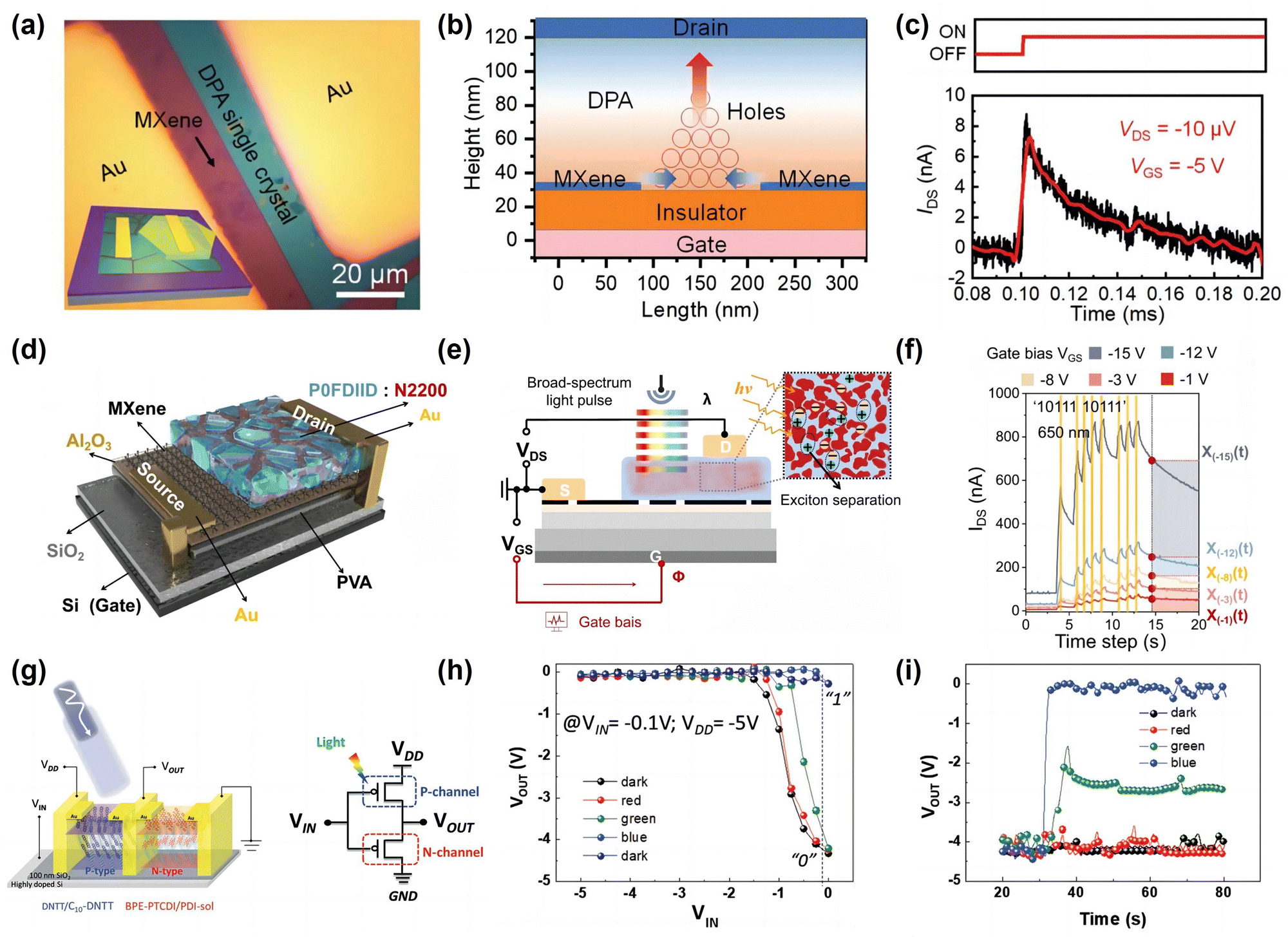 | ||
| Fig. 8 (a) The microscopic image of the MXene–DPA vertical transistor. The inset is the 3D model of the device. (b) A cross-sectional 2D model and the current distribution of VFETs. Holes accumulate at the perforation and then create a pseudoconductive channel. (c) The synaptic behavior of VFET. Reproduced with permission.98 Copyright 2022, Wiley-VCH. (d) Structure diagram of VOFET-DR. (e) Schematic diagram of VOFET-DR operation. (f) At different VGS biases, the device is fed the output current after the optical sequence pulse (650 nm). Reproduced with permission.99 Copyright 2024, Springer Nature. (g) Hole-controlled inverter (device and circuit configuration). (h) and (i) Characteristics of the output voltage under R, B, and G. Reproduced with permission.100 Copyright 2021 Wiley-VCH. | ||
The human visual system undertakes perceiving, learning, and memory, the transduction of visual information (the color and intensity of the light) into neural signals is perception and synapses with STP and LTP are the foundation for learning and memory. Therefore, in order to imitate image processing, it is necessary to integrate photosensing and photosynapse devices into these systems. However, tremendous development challenges are the serious limitation of single wavelength light response and the complicated structure of the device in artificial visual systems. Recently, Wen-Chang Chen et al. first proposed a novel concept that an organic photosensing inverter device acted as a multiwavelength photodetector and recorder (Fig. 8g), which consisted of an N-type OPST (PDI-sol used as the charge-trapping and tunneling layer, and BPE-PTCDI used as the charge transport layer) and a P-type OPST (C10-DNTT acted as the charge-trapping and tunneling layer and DNTT acted as the charge transport layer). Light-triggered broadband (red/green/blue) response and ultra-fast response (<300 ms) were attained (Fig. 8h and i).103 Nevertheless, the second-to-minute timescale of LTP restricted unreliable nonvolatile memory, multiple-plasticity synapses with tunable temporal characteristics, and efficient sensory-memory systems. To address this issue, Liu et al. introduced an organic ferroelectric/electrochemical photonic synaptic transistor, including P(IID-BT) acting as the channel material, PTCDI-C8/vanadyl phthalocyanine (VOPc) and Pc employed as load resistors, [P(VDF-TrFE)] and [P(VP-EDMAEMAES)] used as the gate dielectric, to demonstrate three types of synapses with different timescales (1 ms to 10![[thin space (1/6-em)]](https://www.rsc.org/images/entities/char_2009.gif) 000 s) and current magnitudes, which depended on electrochemical doping and ferroelectric polarization. Then, the different wavelength photo stimuli were converted to volatile and non-volatile synaptic signals to achieve color recognition.104 More and more device structures are being designed to meet the increasing demands of artificial visual systems, laying the foundation for simulating, extending, and expanding human vision.
000 s) and current magnitudes, which depended on electrochemical doping and ferroelectric polarization. Then, the different wavelength photo stimuli were converted to volatile and non-volatile synaptic signals to achieve color recognition.104 More and more device structures are being designed to meet the increasing demands of artificial visual systems, laying the foundation for simulating, extending, and expanding human vision.
3. Innovative applications
In the past, many studies focused on single-function devices, such as phototransistors and non-volatile memories. However, the implementation of AVSs with great potential in the field of artificial intelligence usually requires both visual perception and neuromorphic functions. Recently, the basic functions of the human visual system have been simulated, including short-term plasticity, long-term plasticity, learning forgetting, and relearning processes. The successful simulation of these functions can achieve image sensing and memory, image contrast enhancement, color recognition, handwritten number recognition, and other functions.105–107 These works have been summarized in previous reviews.27,29,108,109 With the deepening of research, more and more synaptic functions have been realized, such as bidirectional optoelectronic synapses, feedforward photoadaptive behavior, sensitization, habituation, and light-wavelength-dependent EPSC. The realization of these functions broadens the use of OPSTs, and researchers apply these functions to visual active adaptation, image processing, motion detection, and other fields, which promotes the further development of AVSs. We summarize some representative works in detail as shown in Table 1 and the recent innovative applications of OPSTs in the following section 3.| Structure type | Materials | Performance | Application | Ref. | ||||
|---|---|---|---|---|---|---|---|---|
| OSC | Functional materials | E pc/per spike | Wavelength (nm) | Synaptic function | ||||
| Single OSC layer | BTBTT6-syn | — | — | 370 | EPSC; LTP | Motion detection | 53 | |
| Dif-TES-ADT | — | 0.07 fJ | 385–540 | EPSC; PPF; STP to LTP transition | Image recognition and reinforcement learning | 58 | ||
| HTEB | — | 4.29 fJ | 365 | EPSC; PPF; LTP; learning and forgetting | — | 60 | ||
| Bulk heterojunction | DPPDTT | MI matrix | 12.3 aJ | 400 | EPSC; PPF; STM to LTM transition | Image preprocess | 70 | |
| DPPDTT | Cl-HABI | 3 fJ | 240–400 | EPSC; PPF; STP to LTP transition | Image preprocess | 69 | ||
| P3HT | CsPbBr3 NPL | 0.053 fJ | 405, 520, 620 | EPSC; PPF; STP to LTP transition | Drosophila's evasive behavior | 66 | ||
| PDPP4T | Chlorophyll | 0.25 fJ | 430 | EPSC; PPF; STP to LTP transition; learning and forgetting | Pattern recognition | 67 | ||
| DPPDTT | CsPbBr3 QDS | 0.4 pJ | 400–650 | EPSC; PPF; STP to LTP transition; logic functions | Pattern recognition | 63 | ||
| Plane heterojunction | DTT-8/TFTCN | — | — | 365 | EPSC; PPF; STP to LTP transition; bidirectional optoelectronic synapses | Motion detection | 29 | |
| Perylene | Graphene oxide | — | 365–1550 | EPSC; PPF; STP to LTP transition; learning and forgetting | Image memorization and recognition | 83 | ||
| DPPDTT | CsPbBr3 QDs | 27.9 aJ | 450 | EPSC; PPF; STP to LTP transition | Motion detection | 27 | ||
| PDPP-DTT/C6Si | PbS QDs | — | 850, 980, 1100, 1550 | EPSC; PPF; STP to LTP transition; learning and forgetting | Visual active adaptation | 81 | ||
| Pentacene | TFB | 0.03 fJ | 365 | EPSC; PPF; STM to LTM transition | The imaging of the retina; pupil contraction process | 85 | ||
| Floating gate | IDTBT | P0FDIID/N2200 | — | White light | Feedforward photoadaptive behavior; sensitization and habituation | Process static and dynamic information | 109 | |
| Pentacene | Zr-CsPbI3/PMMA | — | 405, 520, 650 | Light-wavelength-dependent EPSC | Color information extraction; pattern recognition | 95 | ||
| Pentacene | PbS QDs/PMMA | 0.55 fJ | 365, 550, 850 | EPSC; PPF; STP to LTP transition; learning and forgetting; high-pass filtering behavior | Imaging function | 94 | ||
| PDVT-10 | CdSe/ZnS/P(VDFTrFE) | — | 365, 520, 650 | EPSC; PPF; selective attention under polarization | Image attention processing and pattern classification | 107 | ||
| Pentacene | C3N4 | 18 fJ | 365, 460, 520, 625 | EPSC; PPF; STP to LTP transition | Smart windows | 92 | ||
| Vertical transistor | DPA | MXene | 8.7 aJ | 310, 365, 405, 450 | EPSC; PPF | Multilevel information decoding | 98 | |
| P0FDIID/N2200 | MXene | — | 310, 450, 525, 650, 808 | Nonlinear response and short-term memory characteristics; nonlinear mapping of multi-bit signals | Satellite remote sensing image recognition; traffic trajectory prediction | 99 | ||
3.1. Visual active adaptation
Visual active adaptation is one of the significant functions of the human visual system, that is, under the action of external environmental stimuli, human eyes will make corresponding adjustments according to the stimulus response to adapt to the changes in the environment. In 2021, Di et al. designed two complementary heterojunctions with both transient photo response and dynamic adaptability, and the visual active adaptation was realized finally in the same device. They constructed a flexible 3 × 3 array capable of generating spatially resolved images before and after exposure to strong light (Fig. 9). When the stimulus light was turned on in a dark background, it could be clearly distinguished by a high contrast T-shaped image due to the transient light response of the current. In a strong light background, T-shaped letters appeared within 2 seconds due to current attenuation under light.70 This adaptive mechanism provides a possible way to realize the unique carrier modulation function in crystals and the development of intelligent photo adaptive transistors. The artificial visual system that can operate in the short-wave infrared region (SIR) has enormous application value in fields such as night imaging, autonomous safe driving, military encryption, biomedical, etc. Especially, the SIR artificial visual system that can independently improve processing speed and adapt to different environmental brightness has extraordinary significance. Liu et al. fabricated a 5 × 12 PDPP:C6 Si/PbS OPST array on silicon wafers, which exhibited good mobility uniformity and potential for large-scale imaging applications. Due to the fact that PbS can capture a certain amount of electrons in a white light environment, the PbS QDs have a higher ability to capture electrons when exposed to infrared light in a dark environment than when exposed to infrared light simultaneously in a white light environment. Nonetheless, the device can generate an increase in photocurrent in environments with different light intensities, and the PPF index does not differ significantly in different environments, indicating that the device has better anti-interference ability. To demonstrate the adaptability of the device to ambient light, under dark conditions and different white light intensities, the device was continuously illuminated with 1100 nm SIR light through a mask with a “SIR” shape. In the dark state, the EPSC value at the center of the array was greater than that at the periphery, which clearly presented the SIR pattern. Under 200 cd m−2 white ambient light, the EPSC value of the array slightly decreases. Under 500 cd m−2 white ambient light, the photocurrent value of the array further decreases, but the “SIR” pattern was still presented.84 The results indicated that the array was imaged clearly under the illumination of SIR in both dark and strong light environments, successfully simulating the adaptive and anti-interference abilities of human vision.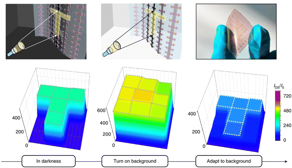 | ||
| Fig. 9 Biomimetic visual perception ability of OAATs. Reproduced with permission.73 Copyright 2021, Springer Nature. | ||
3.2. Image processing
As one of the most important sensory organs in humans, the visual system receives over 80% of external environmental information through the brain every day. The ability to simulate real-time perception and processing of the human visual system has opened up new ideas for the development of efficient AVSs for image processing. Traditional image processing systems are usually physically separated image sensing and processing units, which are limited by communication delays, low processing efficiency, and high energy consumption, and cannot meet the growing demand for efficient image processing. In contrast, the human retina can rely on powerful neural networks to process a large amount of image information in parallel with extremely low energy consumption. Jie et al. developed an ultra-low energy consumption all solution printed OPST array, demonstrating extraordinary neuromorphic photo perception ability and image reinforcement learning capabilities. Based on the test results of the array, the training evolution process of facial image information enhancement was simulated using Python. As the number of training sessions increases (i.e., the number of light pulses increases), more facial information is presented (Fig. 10a).60 The AVS network constructed from an OPST array printed in full solution, as reported in this work, achieved excellent image recognition and enhancement capabilities with low energy consumption. The human visual system needs to quickly switch between filtering and recognition when processing large amounts of unstructured data, and wavelength tuning STP to LTP behavior is crucial for effectively filtering and recognizing targets from complex environments. STP filters out redundant information from a large amount of information, while LTP achieves contrast enhancement of useful information. Huang et al. designed a floating gate OPST based on Zr-CsPbI3, which exhibited different memory modes for different colors of light. Red and green light were STP, while blue light was LTP. Based on this feature, they achieved effective extraction of target information using OPST arrays. By sampling the R, G, and B components of the initial color image, a sensor array was used to extract the bluebird pattern in the image. Due to the different wavelength memory behaviors of devices, as the number of pulses increases, the contrast between blue features and other features is enhanced, and the target of the bird gradually becomes clear (Fig. 10b).99 Similar to the above, Chen et al. proposed a programmable ferroelectric floating gate OPST to simulate selective attention. Under forward polarization, the device had wavelength dependent response intensity, achieving image attention processing for artificial visual perception arrays. The image contained blue “butterflies” and green “leaves”. The high response intensity of the device to blue light and the low response intensity to green light highlighted the characteristics of the butterfly while suppressing the characteristics of the leaves. After a period of time, the features of the “leaves” completely disappeared, and the “butterfly” was extracted.110 Bidirectional synaptic behavior leads to a greater difference in conductivity between different devices, allowing for the acquisition of more graphic feature information. Sun et al. used two different OPSTs with negative photoconductivity and positive photoconductivity (i.e. InGaAs/C8-BTBT and InGaAs/PC61BM) to construct arrays to define hardware cores. An array of 9 PPC and 9 NPC devices was constructed, and according to Kirchhoff's law, the final output current (Ioutput) was the sum of the current of the PPC devices and the current of the NPC devices. One pair of positive and negative photoconductive devices was considered a complete device. Therefore, the “On”-response and “Off”-response existed in a kernel array, and three different image processing methods were achieved by modulating the conductivity value of each device with different irradiation wavelengths. In this case, the inversion, edges, and reliefs of the convolutional kernel (3 × 3) were mapped to the hardware kernel array. The software simulation results reproduced the image features (Fig. 10c).111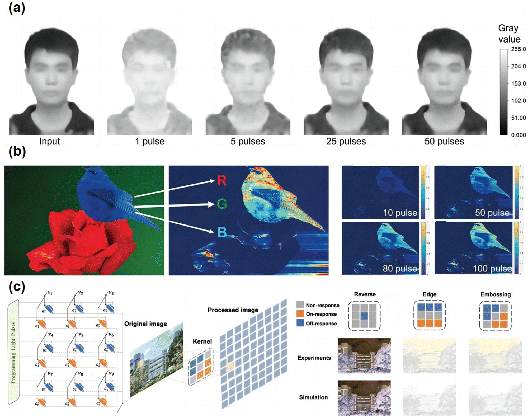 | ||
| Fig. 10 (a) Simulated learning results of a human face based on measured gray value information transformed from ΔW of the FSP-OFET devices. Reproduced with permission.58 Copyright 2022, Wiley-VCH. (b) Implementation of color information extraction using the neuromorphic vision sensor array. Reproduced with permission.95 Copyright 2023, Wiley-VCH. (c) The hardware kernel for simulating the visual processing and recognition functions of the human eye is based on NPC and PPC devices. Reproduced with permission.108 Copyright 2022 Wiley-VCH. | ||
3.3. Motion detection
Machine vision systems can perceive the external environment in real time, perform intelligent analysis from the obtained images, and fetch effective information, the demand of which in human life is increasing, such as driving assistance, medical imaging, security monitoring, urban positioning, etc. Traditional machine vision systems based on the von Neumann architecture face the problem of physical separation between perception units and processing units, resulting in high power consumption and slow response speed. Inspired by the human visual system, neuromorphic devices with image perception, parallel processing, and storage memory functions have emerged. As a fundamental module of neuromorphic devices, OPSTs, which combine visual perception and computational capabilities, are expected to meet the requirements of machine vision.The OPST array can encode the geometric shape and motion trajectory of objects into the shape and color depth of the array's current heatmap, respectively, to achieve effective motion detection. Huang et al. prepared a perovskite quantum dot/OSC microstructure array, scanning the device array at a speed of one pixel per second using humanoid shaped light and recording the current magnitude of the array. The devices exposed to light stimulation for a longer time generate larger currents and darker colors in the heat map. After a period of time, different currents are attained by different light stimulation sequences, which can not only obtain image information from the array but also temporal information about light stimulation. Then, they designed a neural network for motion detection to analyze images and decode information. By inputting the time-varying current information of all pixels into a neural network for processing, the direction of object motion can be determined. Five image datasets, including move up (U), move down (D), move left (L), move right (R), and no objects (N), are created (Fig. 11a).28 After 25 epochs of training, the recognition accuracy can exceed 90%. Based on the same principle, our research group demonstrated the motion detection of petals and pistils by utilizing the ultraviolet ultra-sensitive characteristics of BTBTT6-syn-OPST devices, which can recognize static and dynamic objects. The difference of the UV perceived and stored image brightness between the time t and t + Δt was calculated. For the static objects, the brightness was suppressed to almost zero. For moving objects, the output image brightness contained information about the moving object during the two time periods (Fig. 11b).55 In addition, the heterojunction device of 2DMC prepared by our research group demonstrated the detection of the pendulum swing process through 10 consecutive moments for analysis. In the process of motion detection, the pendulum is regarded as a light signal, and when the pendulum passes by, the device array can receive light pulses. When a series of optical pulse signals are applied to the device array, each pixel outputs different current signals at different times, and then motion detection is achieved by subtracting the signals at different times.30 It is worth noting that bidirectional optoelectronic synapses based on 2DMC heterojunctions can achieve high contrast motion detection, which is crucial for reducing environmental noise interference and improving recognition accuracy.
 | ||
| Fig. 11 (a) Projected images of an arrow moving from left to right at various times in a 10 × 10 neuromorphic photosensor array and a schematic diagram of the neuromorphic photosensor array in conjunction with a neural network. Reproduced with permission.27 Copyright 2024, Wiley-VCH. (b) Illustration of motion detection with the BTBTT6-syn-based synaptic OPT arrays. Reproduced with permission.53 Copyright 2023, Springer Nature. | ||
Road traffic trajectory prediction, as a time series signal task, is an important application of machine vision, and accurately predicting different spatiotemporal characteristic signals remains a challenge. On the basis of the above research, our research group further implemented a motion target extraction network based on 2DMC heterojunction bidirectional OPSTs. The process of extracting moving targets was demonstrated. The network comprised N × M pixels, with each pixel module consisting of bidirectional synapse mode 2DMC heterojunction OPST. The motion detection of moving vehicles on the road at different times was demonstrated, which was successfully marked. In addition, the completed labeled image was input into a pre-trained convolutional neural network (CNN) to identify the labeled objects. The network accurately recognized eight classic objects, including people, bicycles, motorcycles, cars, etc. with an accuracy rate of over 90% in road traffic, which indicated that the network based on 2DMC heterojunction OPSTs had a motion detection function (Fig. 12a).30
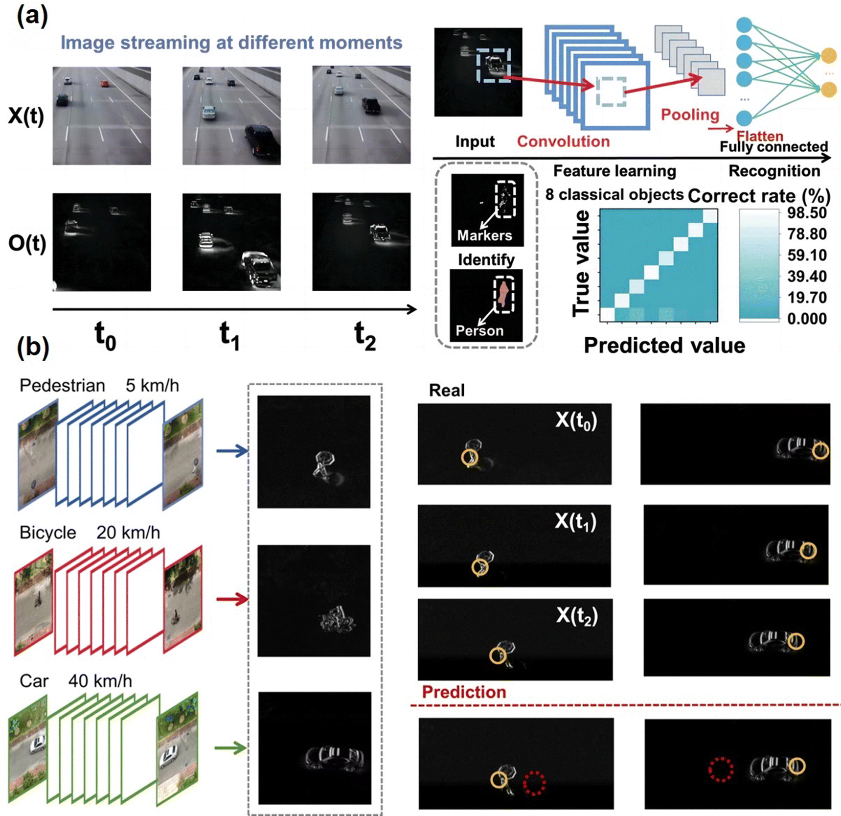 | ||
| Fig. 12 (a) Motion detection of moving vehicles on the road at different moments and recognition of the tagged objects with an already trained convolutional neural network (CNN). Reproduced with permission.29 Copyright 2023, Wiley-VCH. (b) The spatial frame information of different traffic elements and the velocity and coordinate information of the object in the previous three frames as input and output to train the encoding system. Reproduced with permission.99 Copyright 2024, Springer Nature. | ||
However, most current devices rely on linear models to process optoelectronic signals, which limits the computational efficiency of neural networks and the adaptability to static and dynamic information. It is necessary to develop new models that can handle nonlinear signals effectively. Chen et al. constructed a feedforward photonic adaptive OPST by coupling the gate potential with the space charge potential. The OPST exhibited sequential photoexcitation and photoinhibition at constant light intensity, transforming the device from a linear to a nonlinear model. Supported by the performance of this device, it can reduce interference caused by various nonlinear light intensity factors. The system processed dynamic information under the interference of different light intensities, and the processed image information was successfully segmented and recognized by the backend neural network. The recognition accuracy of 21 types of information exceeded 90%.112
In addition, traffic roads, due to the varying movement rates of different traffic parts such as pedestrians, bicycles, and cars, generate diverse temporal and spatial frame information flows. The different spatiotemporal feature signals contained in these flows pose challenges to accurate prediction. Chen et al. used the optical flow method and inter-frame difference method to acquire the motion trajectory (spatial frame information) and motion rate (temporal frame information) of moving objects, respectively. Based on the short-term memory effect by light stimuli of their constructed VOFET-OPST, the memory current generated by a moving object at the previous time position gradually decreased over time and formed an intensity difference with the memory current at the present time position, which recognized the trajectory of the object. In addition, by modulating the gate voltage of the VOFET-OPST to change its attenuation characteristics, it adapted to traffic factors with different speeds. The system for encoding, constructed using the speed and orientation information obtained above, predicted the future frames of the moving object. The movement trajectories of pedestrians, bicycles, and cars, with good overlap with actual trajectories, were successfully predicted. The VOFET-OPST with a nanoscale transport distance improves the transport efficiency of photo-generated charges and provides richer modulation through external stimuli. The non-uniform gate field precisely regulates charge transport, avoiding the problem of low charge transfer efficiency. Then, the level of traps has a significant impact on the decay time. The use of light pulses of different wavelengths to induce photo-generated charges in different levels effectively expands the time scale of the device (Fig. 12b).102
4. Conclusions and outlook
In summary, with the accelerated development of artificial intelligence technology, research on AVSs has received increasing attention and has achieved many excellent successes. One of the basic components of AVSs is OPST, which plays a dual role in light sensing and light synapses. The development of high-performance OPSTs has become a research hotspot, so this article focuses on the structures and applications based on OPSTs, explains the working mechanisms of different structures, summarizes the functional materials used in different device structures, narrates diverse device functions and introduces innovative applications based on OPSTs. These works have laid a solid foundation for the development of AVSs.In addition, we put forward some forward-looking views on this developing and challenging field to provide some potential future research directions and opportunities:
(i) Research on the charge trapping mechanism: charge traps are widely presented in the composition and structure of various parts of transistors, and are easily unintentionally introduced. Defects, impurities, grain boundaries, polar groups, conductive centers, etc. in transistors can all serve as potential charge traps, which pose great challenges for understanding and utilizing charge trapping mechanisms. There are relatively few reports on the working mechanism of OPSTs, and the explanation of their working mechanism is only from the perspective of the energy band or trap capture, lacking experimental results to support the response. Therefore, it is necessary to conduct in-depth research on the charge trapping mechanism and design effective introduction strategies to develop OPSTs with excellent conductivity regulation memory ability and multi-field collaborative regulation.
(ii) Developing low power consumption OPSTs: currently, OPSTs applied in the field of neuromorphic electronics still face two significant challenges in reducing power consumption. On the one hand, OPSTs often use a high k dielectric layer to effectively reduce the operating voltage of the device. However, the strong dipole polarization effect of the high k dielectric layer will lead to a significant decrease in charge transfer performance, affecting the response and computational speed of the device in future applications. On the other hand, OPSTs often use polycrystalline or amorphous OSC films, which are usually thicker, resulting in gate control not being able to put them in a completely depleted mode. Additionally, there are numerous defects, grain boundaries, and traps inside the films, which make it difficult to reduce the off-state current of OPSTs. Therefore, achieving low operating current, low operating voltage, high response speed, and power consumption for OPSTs is still a highly challenging task.
(iii) Developing wide spectrum response OPSTs: heterojunctions can achieve unique optoelectronic properties by using different functional components cooperatively, but there are still major challenges in their preparation and processing technology. Although OSCs can easily obtain large-area films by solution processing, the vulnerability of OSC layers to organic solvents makes them easy to dissolve during subsequent layer-by-layer preparation, which limits the practicability of large-scale device manufacturing and competitive applications. At present, it has been reported that the methods used to solve this problem have the problems of complex processes and lack of universality. Therefore, developing a general and simple stacking process to prepare heterojunction structures, in addition, we can synthesize OSC materials with wide spectrum absorption by reasonably designing the molecular structure to achieve wide spectrum response OPSTs.
(iv) Developing large-area OPST array devices: at present, the preparation of large-area and high-density device arrays is inevitable to repeatedly deposit various functional materials to prepare device arrays, which requires a patterning strategy compatible with lithography. Therefore, it is urgent to develop a solution processing technology suitable for the preparation of large-area array devices, such as patterned hydrophilic and hydrophobic regions, and the preparation of device arrays with high density, high uniformity, and high yield.
(v) Realizing a neuromorphic visual device integrating sense, memory, and computing: it is an urgent need in the field of artificial intelligence to realize multi-mode information recognition and deal with the external environment information efficiently and comprehensively. At present, neuromorphic devices are widely used in bionic electronics and artificial intelligence computing. In the future, neuromorphic devices are expected to be more intelligent and humanized and should be directly used for robot human interaction. However, the current reported work mainly focuses on the simulation of human common memory behavior and single MNIST pattern recognition tasks, which limits the further integration and construction of artificial neural networks to achieve progress in the fields of bionic robots, artificial eyes, and so on. Therefore, neural networks suitable for different applications are developed by using the performance characteristics of the devices. In addition, the display is endowed with intelligent functions, which can be applied to intelligent image processing and intelligent interactive display, and realize the combination of future display and artificial intelligence technology.
Although OPSTs have been studied for many years, they are still in the primary stage. It is expected that the integration of multiple disciplines will promote the vigorous development of this field. We believe that more exciting achievements will be demonstrated in the near future. This review summarizes the recent signs of progress and advances of OPSTs and hopes to inspire future research in this field.
Author contributions
Yiwen Ren: writing the original draft. Yidi Xie, Shaosong Gao, Yuhan Du, Ming Zhang, Xianshuo Wu, and Xiaoting Zhu revising the original draft. Lingjie Sun: conceiving and supervising this study. Fangxu Yang: supervision.: supervision. Wenping Hu: investigation.Conflicts of interest
There are no conflicts to declare.Acknowledgements
The authors thank the National Key R&D Program (2022YFB3607500 and 2022YFB3603800), the National Natural Science Foundation (no. 52373194), and the open research fund from State Key Laboratory of Luminescent Materials and Devices (2023-skllmd-02).References
- S. Zhu, Y. Li, H. Yelemulati, X. Deng, Y. Li, J. Wang, X. Li, G. Li, P. Gkoupidenis and Y. Tai, Sci. Adv., 2022, 8, eabo5314 CrossRef CAS PubMed
.
- M. Yip, S. Salcudean, K. Goldberg, K. Althoefer, A. Menciassi, J. Opferman, A. Krieger, K. Swaminathan, C. Walsh, H. Huang and I. Lee, Science, 2023, 381, 141–146 CrossRef CAS PubMed
- F. Zhou, Z. Zhou, J. Chen, T. H. Choy, J. Wang, N. Zhang, Z. Lin, S. Yu, J. Kang, H. S. P. Wong and Y. Chai, Nat. Nanotechnol., 2019, 14, 776–782 CrossRef CAS PubMed
- L. Mennel, J. Symonowicz, S. Wachter, D. K. Polyushkin, A. J. Molina-Mendoza and T. Mueller, Nature, 2020, 579, 62–66 CrossRef CAS PubMed
- Y. Chai, Nature, 2020, 579, 32–33 CrossRef CAS PubMed
- F. Ashtiani, A. J. Geers and F. Aflatouni, Nature, 2022, 606, 501–506 CrossRef CAS PubMed
- H. Ning, Z. Yu, Q. Zhang, H. Wen, B. Gao, Y. Mao, Y. Li, Y. Zhou, Y. Zhou, J. Chen, L. Liu, W. Wang, T. Li, Y. Li, W. Meng, W. Li, Y. Li, H. Qiu, Y. Shi, Y. Chai, H. Wu and X. Wang, Nat. Nanotechnol., 2023, 18, 493–500 CrossRef CAS PubMed
- X. Huang, C. Liu, Z. Tang, S. Zeng, S. Wang and P. Zhou, Nat. Nanotechnol., 2023, 18, 486–492 CrossRef CAS PubMed
- J. Chen, Z. Zhou, B. J. Kim, Y. Zhou, Z. Wang, T. Wan, J. Yan, J. Kang, J.-H. Ahn and Y. Chai, Nat. Nanotechnol., 2023, 18, 882–888 CrossRef CAS PubMed
- F. Liao, Z. Zhou, B. J. Kim, J. Chen, J. Wang, T. Wan, Y. Zhou, A. T. Hoang, C. Wang, J. Kang, J.-H. Ahn and Y. Chai, Nat. Electron., 2022, 5, 84–91 CrossRef
- K. Liu, T. Zhang, B. Dang, L. Bao, L. Xu, C. Cheng, Z. Yang, R. Huang and Y. Yang, Nat. Electron., 2022, 5, 761–773 CrossRef CAS
- R. Juliano Martins, E. Marinov, M. A. B. Youssef, C. Kyrou, M. Joubert, C. Colmagro, V. Gâté, C. Turbil, P.-M. Coulon, D. Turover, S. Khadir, M. Giudici, C. Klitis, M. Sorel and P. Genevet, Nat. Commun., 2022, 13, 5724 CrossRef CAS PubMed
- W. Li, Q. Ma, C. Liu, Y. Zhang, X. Wu, J. Wang, S. Gao, T. Qiu, T. Liu, Q. Xiao, J. Wei, T. T. Gu, Z. Zhou, F. Li, Q. Cheng, L. Li, W. Tang and T. J. Cui, Nat. Commun., 2023, 14, 989 CrossRef CAS PubMed
- Y. Ren, X. Bu, M. Wang, Y. Gong, J. Wang, Y. Yang, G. Li, M. Zhang, Y. Zhou and S.-T. Han, Nat. Commun., 2022, 13, 5585 CrossRef CAS PubMed
- A. Dodda, D. Jayachandran, A. Pannone, N. Trainor, S. P. Stepanoff, M. A. Steves, S. S. Radhakrishnan, S. Bachu, C. W. Ordonez, J. R. Shallenberger, J. M. Redwing, K. L. Knappenberger, D. E. Wolfe and S. Das, Nat. Mater., 2022, 21, 1379–1387 CrossRef CAS PubMed
- Z. Cheng, C. Ríos, W. H. P. Pernice, C. D. Wright and H. Bhaskaran, Sci. Adv., 2017, 3, e1700160 CrossRef PubMed
- T. Tuma, A. Pantazi, M. Le Gallo, A. Sebastian and E. Eleftheriou, Nat. Nanotechnol., 2016, 11, 693–699 CrossRef CAS PubMed
- C. Chen, Y. He, H. Mao, L. Zhu, X. Wang, Y. Zhu, Y. Zhu, Y. Shi, C. Wan and Q. Wan, Adv. Mater., 2022, 34, 2201895 CrossRef CAS PubMed
- F. Yang, L. Sun, Q. Duan, H. Dong, Z. Jing, Y. Yang, R. Li, X. Zhang, W. Hu and L. Chua, SmartMat, 2021, 2, 99–108 CrossRef CAS
- M. E. Pereira, R. Martins, E. Fortunato, P. Barquinha and A. Kiazadeh, Neuromorphic Comput. Eng., 2023, 3, 022002 CrossRef
- Y. Zhou, J. Fu, Z. Chen, F. Zhuge, Y. Wang, J. Yan, S. Ma, L. Xu, H. Yuan, M. Chan, X. Miao, Y. He and Y. Chai, Nat. Electron., 2023, 6, 870–878 CrossRef
- Z. Zhang, S. Wang, C. Liu, R. Xie, W. Hu and P. Zhou, Nat. Nanotechnol., 2021, 17, 27–32 CrossRef PubMed
- C. Choi, J. Leem, M. Kim, A. Taqieddin, C. Cho, K. W. Cho, G. J. Lee, H. Seung, H. J. Bae, Y. M. Song, T. Hyeon, N. R. Aluru, S. Nam and D.-H. Kim, Nat. Commun., 2020, 11, 5934 CrossRef CAS PubMed
- D. Zhu and D. Ji, SmartMat, 2023, 4, e1179 CrossRef CAS
- X. Wang, Y. Lu, J. Zhang, S. Zhang, T. Chen, Q. Ou and J. Huang, Small, 2020, 17, 2005491 CrossRef PubMed
- T. Park, M. Kim, E. K. Lee, J. Hur and H. Yoo, Small, 2023, 20, 2306468 CrossRef PubMed
- Q. Zhang, T. Jin, X. Ye, D. Geng, W. Chen and W. Hu, Adv. Funct. Mater., 2021, 31, 2106151 CrossRef CAS
- Y. Wu, S. Dai, X. Liu, P. Guo, J. Zhang, T. Sun, Z. Guo, Y. Xu, H. Liang, L. Xiong, H. Hu and J. Huang, Adv. Funct. Mater., 2024, 2315175 CrossRef CAS
- S. Dai, X. Liu, Y. Liu, Y. Xu, J. Zhang, Y. Wu, P. Cheng, L. Xiong and J. Huang, Adv. Mater., 2023, 35, 2300329 CrossRef CAS PubMed
- X. Zhu, C. Gao, Y. Ren, X. Zhang, E. Li, C. Wang, F. Yang, J. Wu, W. Hu and H. Chen, Adv. Mater., 2023, 35, 2301468 CrossRef CAS PubMed
- X. Wang, S. Yang, Z. Qin, B. Hu, L. Bu and G. Lu, Adv. Mater., 2023, 35, 2300329 CrossRef PubMed
- B. Fu, F. Yang, L. Sun, Q. Zhao, D. Ji, Y. Sun, X. Zhang and W. Hu, Adv. Mater., 2022, 34, 2203330 CrossRef CAS PubMed
- L. Shan, Q. Chen, R. Yu, C. Gao, L. Liu, T. Guo and H. Chen, Nat. Commun., 2023, 14, 2648 CrossRef CAS PubMed
- B. He, G. He, C. Fu, S. Jiang, E. Fortunato, R. Martins and S. Wang, Adv. Funct. Mater., 2024, 2316375 CrossRef
- L. Liu, Q. Chen, H. Zeng, L. Shan, C. An, B. Zhuang, H. Chen, T. Guo and W. Hu, Adv. Mater. Technol., 2023, 8, 2300225 CrossRef CAS
- L. Shan, R. Yu, Z. Chen, X. Zhang, C. Gao, M. Lian, Y. Hu, T. Guo and H. Chen, Adv. Funct. Mater., 2024, 2315584 CrossRef
- Z. Chen, R. Yu, X. Yu, E. Li, C. Wang, Y. Liu, T. Guo and H. Chen, ACS Nano, 2022, 16, 19155–19164 CrossRef CAS PubMed
- K. Chen, H. Hu, I. Song, H. B. Gobeze, W.-J. Lee, A. Abtahi, K. S. Schanze and J. Mei, Nat. Photonics, 2023, 17, 629–637 CrossRef CAS
- T. Jiang, Y. Wang, W. Huang, H. Ling, G. Tian, Y. Deng, Y. Geng, D. Ji and W. Hu, Light: Sci. Appl., 2023, 12, 264 CrossRef CAS PubMed
- H. Shen, Z. He, W. Jin, L. Xiang, W. Zhao, C. A. Di and D. Zhu, Adv. Mater., 2019, 31, 1905018 CrossRef CAS PubMed
- S. M. Kwon, S. W. Cho, M. Kim, J. S. Heo, Y. H. Kim and S. K. Park, Adv. Mater., 2019, 31, 1906433 CrossRef CAS PubMed
- D. Li, H. Ren, Y. Chen, Y. Tang, K. Liang, Y. Wang, F. Li, G. Liu, L. Meng and B. Zhu, Adv. Funct. Mater., 2023, 33, 2303198 CrossRef CAS
- J. Yao, L. Sun, Y. Xiao, J. Liu, J. Jie, X. Liu, F. Yang, Y. Sun, R. Li and W. Hu, Sci. China Mater., 2022, 66, 1511–1517 CrossRef
- J. Yao, Y. Zhang, X. Tian, X. Zhang, H. Zhao, X. Zhang, J. Jie, X. Wang, R. Li and W. Hu, Angew. Chem., Int. Ed., 2019, 58, 16082–16086 CrossRef CAS PubMed
- Y. Zheng, S. Zhang, J. B. H. Tok and Z. Bao, J. Am. Chem. Soc., 2022, 144, 4699–4715 CrossRef CAS PubMed
- Q. Zhang, X. Ye, Y. Zheng, Y. Wang, L. Li, Z. Gao, J. Wu, H. Dong, D. Geng and W. Hu, J. Mater. Chem. C, 2022, 10, 2681–2689 RSC
- C. An, W. Dong, R. Yu, C. Xu, D. Pei, X. Wang, H. Chen, C. Chi, Y. Han and Y. Geng, Chem. Mater., 2023, 36, 450–460 CrossRef
- C. Yang, J. Qian, S. Jiang, H. Wang, Q. Wang, Q. Wan, P. K. L. Chan, Y. Shi and Y. Li, Adv. Opt. Mater., 2020, 8, 2000153 CrossRef CAS
- F. Yang, L. Jin, L. Sun, X. Ren, X. Duan, H. Cheng, Y. Xu, X. Zhang, Z. Lai, W. Chen, H. Dong and W. Hu, Adv. Mater., 2018, 30, 1801891 CrossRef PubMed
- S. Li, Z. Zhang, X. Chen, W. Deng, Y. Lu, M. Sui, F. Gong, G. Xu, X. Li, F. Liu, C. You, F. Chu, Y. Wu, H. Yan and Y. Zhang, Adv. Mater., 2022, 34, 2107734 CrossRef CAS PubMed
- M. Farronato, P. Mannocci, M. Melegari, S. Ricci, C. M. Compagnoni and D. Ielmini, Adv. Mater., 2022, 35, 2205381 CrossRef PubMed
- L. Fang, S. Dai, Y. Zhao, D. Liu and J. Huang, Adv. Electron. Mater., 2019, 6, 1901217 CrossRef
- X. Wu, D. Dai, Y. Ling, S. Chen, C. Huang, S. Feng and W. Huang, ACS Appl. Mater. Interfaces, 2020, 12, 30627–30634 CrossRef CAS PubMed
- L. Zhu, J. Zhang, Y. Guo, C. Yang, Y. Yi and Z. Wei, Angew. Chem., Int. Ed., 2021, 60, 15348–15353 CrossRef CAS PubMed
- T. Jiang, Y. Wang, Y. Zheng, L. Wang, X. He, L. Li, Y. Deng, H. Dong, H. Tian, Y. Geng, L. Xie, Y. Lei, H. Ling, D. Ji and W. Hu, Nat. Commun., 2023, 14, 2281 CrossRef CAS PubMed
- Y. C. Xiaohan Wu, R. Liu, H. E. Katz and Jia Huang, Adv. Sci., 2017, 4, 1700442 CrossRef PubMed
- S. Dai, D. Liu, Y. Chu, K. Wang, B. Yang and J. Huang, ACS Appl. Mater. Interfaces, 2018, 10, 21472–21480 CrossRef CAS PubMed
- Y. Zhao, S. Dai, D. Liu, L. Fang, Z. Liu and J. Huang, Org. Electron., 2020, 83, 105749 CrossRef CAS
- J. Shi, J. Jie, W. Deng, G. Luo, X. Fang, Y. Xiao, Y. Zhang, X. Zhang and X. Zhang, Adv. Mater., 2022, 34, 2200380 CrossRef CAS PubMed
- R. Jia, X. Wu, W. Deng, X. Zhang, L. Huang, K. Niu, L. Chi and J. Jie, Adv. Funct. Mater., 2019, 29, 1905657 CrossRef CAS
- L. Zhang, X. Tian, J. Yao, X. Song, S. Yang, S. Guo, Y. Wang, B. Li, X. Ren, Y. Sun, F. Yang, R. Li and W. Hu, J. Mater. Chem. C, 2021, 9, 8834–8841 RSC
- Z. Hua, B. Yang, J. Zhang, D. Hao, P. Guo, J. Liu, L. Jiang and J. Huang, Nano Res., 2022, 15, 7639–7645 CrossRef CAS
- D. Xue, Q. Wang, M. Xie, W. Gong, Y. Zhang, Y. Yin, Y. Wei, J. Lu, J. Zhang, S. Duhm, Z. Wang, L. Chi and L. Huang, Adv. Opt. Mater., 2023, 12, 2302091 CrossRef
- K. Wang, S. Dai, Y. Zhao, Y. Wang, C. Liu and J. Huang, Small, 2019, 15, 1900010 CrossRef PubMed
- D. Hao, J. Zhang, S. Dai, J. Zhang and J. Huang, ACS Appl. Mater. Interfaces, 2020, 12, 39487–39495 CrossRef CAS PubMed
- J. Zhang, T. Sun, S. Zeng, D. Hao, B. Yang, S. Dai, D. Liu, L. Xiong, C. Zhao and J. Huang, Nano Energy, 2022, 95, 106987 CrossRef CAS
- J. Y. Chen, D. L. Yang, F. C. Jhuang, Y. H. Fang, J. S. Benas, F. C. Liang and C. C. Kuo, Adv. Funct. Mater., 2021, 31, 2105911 CrossRef CAS
- H. Shao, Y. Li, J. Chen, W. Yang, L. Wang, J. Fu, Y. Wang, H. Ling, L. Xie and W. Huang, SmartMat, 2023, e1230 CrossRef
- S. Lan, Y. Ke and H. Chen, IEEE Electron Device Lett., 2021, 42, 1180–1183 CAS
- Z. He, H. Shen, D. Ye, L. Xiang, W. Zhao, J. Ding, F. Zhang, C.-A. Di and D. Zhu, Nat. Electron., 2021, 4, 522–529 CrossRef CAS
- B. Yang, Y. Lu, D. Jiang, Z. Li, Y. Zeng, S. Zhang, Y. Ye, Z. Liu, Q. Ou, Y. Wang, S. Dai, Y. Yi and J. Huang, Adv. Mater., 2020, 32, 2001227 CrossRef CAS PubMed
- J. Zhang, D. Liu, Q. Shi, B. Yang, P. Guo, L. Fang, S. Dai, L. Xiong and J. Huang, npj Flex. Electron., 2022, 6, 30 CrossRef CAS
- B. Yang, Y. Wang, Z. Hua, J. Zhang, L. Li, D. Hao, P. Guo, L. Xiong and J. Huang, Chem. Commun., 2021, 57, 8300–8303 RSC
- D. Liu, J. Zhang, Q. Shi, T. Sun, Y. Xu, L. Li, L. Tian, L. Xiong, J. Zhang and J. Huang, Adv. Mater., 2024, 36, 2305370 CrossRef CAS PubMed
- Z. Guo, J. Zhang, B. Yang, L. Li, X. Liu, Y. Xu, Y. Wu, P. Guo, T. Sun, S. Dai, H. Liang, J. Wang, Y. Zou, L. Xiong and J. Huang, Adv. Mater., 2024, 36, 2310155 CrossRef CAS PubMed
- Z. Hao, H. Wang, S. Jiang, J. Qian, X. Xu, Y. Li, M. Pei, B. Zhang, J. Guo, H. Zhao, J. Chen, Y. Tong, J. Wang, X. Wang, Y. Shi and Y. Li, Adv. Sci., 2022, 9, 2103494 CrossRef CAS PubMed
- D. Hao, Z. Yang, J. Huang and F. Shan, Adv. Funct. Mater., 2022, 33, 2211467 CrossRef
- C. Han, X. Han, J. Han, M. He, S. Peng, C. Zhang, X. Liu, J. Gou and J. Wang, Adv. Funct. Mater., 2022, 32, 2113053 CrossRef CAS
- Z. Guo, J. Zhang, X. Liu, L. Wang, L. Xiong and J. Huang, Adv. Funct. Mater., 2023, 33, 2305508 CrossRef CAS
- J. Liu, Z. Yang, Z. Gong, Z. Shen, Y. Ye, B. Yang, Y. Qiu, B. Ye, L. Xu, T. Guo and S. Xu, ACS Appl. Mater. Interfaces, 2021, 13, 13362–13371 CrossRef CAS PubMed
- X. Huang, Q. Li, W. Shi, K. Liu, Y. Zhang, Y. Liu, X. Wei, Z. Zhao, Y. Guo and Y. Liu, Small, 2021, 17, 2102820 CrossRef CAS PubMed
- J. Kuang, K. Liu, M. Liu, M. Shao, M. Zhu, G. Liu, W. Wen, J. Chen, M. Qin, Z. Pan, Z. Zhao, Y. Liu and Y. Guo, Adv. Funct. Mater., 2022, 33, 2209502 CrossRef
- C. Han, X. Liu, X. Han, M. He, J. Han, H. Zhang, X. Hou, H. Zhou, H. Yu, Z. Wu, J. Gou and J. Wang, Adv. Funct. Mater., 2022, 32, 2209680 CrossRef CAS
- X. Huang, Y. Liu, G. Liu, K. Liu, X. Wei, M. Zhu, W. Wen, Z. Zhao, Y. Guo and Y. Liu, Adv. Funct. Mater., 2022, 33, 2208836 CrossRef
- J. Wang, B. Yang, S. Dai, P. Guo, Y. Gao, L. Li, Z. Guo, J. Zhang, J. Zhang and J. Huang, Adv. Mater. Technol., 2023, 8, 2300449 CrossRef CAS
- H. Zhang, X. Dong, Z. Zhang, Z. Zhang, C. Ban, Z. Zhou, C. Song, S. Yan, Q. Xin, J. Liu, Y. Li and W. Huang, Nat. Commun., 2022, 13, 4996 CrossRef CAS PubMed
- H. Shao, Y. Li, J. Zhuang, Y. Ji, X. He, R. Wang, L. Wang, J. Fu, W. Li, M. Yi, L. Xie, W. Huang and H. Ling, Adv. Funct. Mater., 2024, 2316381 CrossRef CAS
- J. Zhang, Q. Shi, R. Wang, X. Zhang, L. Li, J. Zhang, L. Tian, L. Xiong and J. Huang, InfoMat, 2021, 3, 904–916 CrossRef CAS
- D. Liu, Q. Shi, J. Zhang, L. Tian, L. Xiong, S. Dai and J. Huang, Adv. Intell. Syst., 2022, 4, 2200164 CrossRef
- Q. Shi, D. Liu, S. Dai and J. Huang, Adv. Opt. Mater., 2021, 9, 2100654 CrossRef CAS
- X. Zhu, Y. Yan, L. Sun, Y. Ren, Y. Zhang, Y. Liu, X. Zhang, R. Li, H. Chen, J. Wu, F. Yang and W. Hu, Adv. Mater., 2022, 34, 2201364 CrossRef CAS PubMed
- K. Lee, H. Han, Y. Kim, J. Park, S. Jang, H. Lee, S. W. Lee, H. Kim, Y. Kim, T. Kim, D. Kim, G. Wang and C. Park, Adv. Funct. Mater., 2021, 31, 2105596 CrossRef CAS
- Y. Chen, J. Hua, Y. Li, Q. Zhang, H. Shao, W. Li, H. Ling, X. Xu, W. Huang and M. Yi, Adv. Mater. Technol., 2022, 8, 2201367 CrossRef
- R. Martins, P. Barquinha, L. Pereira, N. Correia, G. Gonçalves, I. Ferreira and E. Fortunato, Phys. Status Solidi RRL, 2009, 3, 308–310 CrossRef CAS
- B. Mu, L. Guo, J. Liao, P. Xie, G. Ding, Z. Lv, Y. Zhou, S. T. Han and Y. Yan, Small, 2021, 17, 2103837 CrossRef CAS PubMed
- H. L. Park, H. Kim, D. Lim, H. Zhou, Y. H. Kim, Y. Lee, S. Park and T. W. Lee, Adv. Mater., 2020, 32, 1906899 CrossRef CAS PubMed
- J. Zhang, P. Guo, Z. Guo, L. Li, T. Sun, D. Liu, L. Tian, G. Zu, L. Xiong, J. Zhang and J. Huang, Adv. Funct. Mater., 2023, 33, 2302885 CrossRef CAS
- J. Zhang, Z. Guo, T. Sun, P. Guo, X. Liu, H. Gao, S. Dai, L. Xiong and J. Huang, SmartMat, 2023, e1246 CrossRef
- H. Shao, Y. Li, W. Yang, X. He, L. Wang, J. Fu, M. Fu, H. Ling, P. Gkoupidenis, F. Yan, L. Xie and W. Huang, Adv. Mater., 2023, 35, 2208497 CrossRef CAS PubMed
- T. Chen, X. Wang, D. Hao, S. Dai, Q. Ou, J. Zhang and J. Huang, Adv. Opt. Mater., 2021, 9, 2002030 CrossRef CAS
- Q. Zhang, E. Li, Y. Wang, C. Gao, C. Wang, L. Li, D. Geng, H. Chen, W. Chen and W. Hu, Adv. Mater., 2022, 35, 2208600 CrossRef PubMed
- C. Gao, D. Liu, C. Xu, W. Xie, X. Zhang, J. Bai, Z. Lin, C. Zhang, Y. Hu, T. Guo and H. Chen, Nat. Commun., 2024, 15, 740 CrossRef CAS PubMed
- C. C. Hung, Y. C. Chiang, Y. C. Lin, Y. C. Chiu and W. C. Chen, Adv. Sci., 2021, 8, 2100742 CrossRef CAS PubMed
- H. Wang, Z. Ni, Q. Li, H. Liu, Y. Yang, L. Wang, Y. Ran, Y. Guo, W. Hu and Y. Liu, Adv. Mater., 2018, 30, 1803961 CrossRef PubMed
- J. Zhang, Y. Lu, S. Dai, R. Wang, D. Hao, S. Zhang, L. Xiong and J. Huang, Research, 2021, 2021, 7131895 CAS
- W. Deng, X. Zhang, R. Jia, L. Huang, X. Zhang and J. Jie, NPG Asia Mater., 2019, 11, 77 CrossRef CAS
- H. Zhang, X. Ju, D. Chi, L. Feng, Z. Liu, K. Yew, M. Zhu, T. Li, R. Wei, S. Wang, L. Sun, Z. Wang and Y. Wu, Appl. Mater. Today, 2023, 33, 101885 CrossRef
- H. Chen, Y. Cai, Y. Han and H. Huang, Angew. Chem., Int. Ed., 2023, 63, e202313634 CrossRef PubMed
- N. Li, S. Zhang, Y. Peng, X. Li, Y. Zhang, C. He and G. Zhang, Adv. Funct. Mater., 2023, 33, 2305589 CrossRef CAS
- R. Yu, L. He, C. Gao, X. Zhang, E. Li, T. Guo, W. Li and H. Chen, Nat. Commun., 2022, 13, 7019 CrossRef PubMed
- P. Xie, X. Chen, Z. Zeng, W. Wang, Y. Meng, Z. Lai, Q. Quan, D. Li, W. Wang, X. Bu, S. W. Tsang, S. Yip, J. Sun and J. C. Ho, Adv. Funct. Mater., 2022, 33, 2209091 CrossRef
- C. Gao, D. Liu, C. Xu, J. Bai, E. Li, X. Zhang, X. Zhu, Y. Hu, Z. Lin, T. Guo and H. Chen, Adv. Funct. Mater., 2024, 2313217 CrossRef CAS
| This journal is © The Royal Society of Chemistry 2024 |