
Recent progress on solar blind deep ultraviolet photodetectors based on metal halide perovskites
Wanfang
Yang
,
Yutian
Lei
and
Zhiwen
Jin
 *
*
School of Physical Science and Technology, Lanzhou University, Lanzhou 730000, China. E-mail: jinzw@lzu.edu.cn
First published on 26th April 2024
Abstract
Solar blind deep ultraviolet photodetectors (DUVPDs) are widely used in civil and military fields, such as partial discharge detection, flame detection and missile guidance. In the past decade, traditional wide band gap semiconductors (such as GaN, Ga2O3, and AlN) have been the dominant material for solar blind detection. Furthermore, they have experienced considerable progress with respect to sensitivity, switching ratio and dark current. As a star material in the photoelectric field, metal halide perovskites (MHPs) have led to some excellent works in the field of solar blind detection. However, the existing reviews in the field of solar blind detection are all based on traditional wide band gap semiconductors, and there is no article summarizing the studies on MHP solar blind detection. Therefore, in this article, beginning with the most basic principles and performance characterization of photodetectors, we introduce the research progress and present situation of solar blind detection based on MHPs. The MHPs discussed in this paper mainly include the lead-based perovskite CsPbX3 (X = Cl, Br, or I) and copper-based perovskites CsCu2I3 and Cs3Cu2I5. Furthermore, the manufacturing strategies, and direct and indirect detection processes of DUVPDs are discussed in detail. At the end of the article, we present a brief outlook that examines the challenges and future strategies for solar blind DUVPDs.
 Zhiwen Jin | Zhiwen Jin is a professor at the School of Physical Science and Technology, Lanzhou University. He received his BS degree from Lanzhou University in 2011 and PhD from the Institute of Chemistry, Chinese Academy of Sciences, in 2016. He has also been listed among “Clarivate's Highly Cited Researchers” and “Elsevier's Most Cited Chinese Researchers”. Since he joined Lanzhou University as a principal investigator, his main research direction has been X-ray detection and imaging technology based on metal halides. |
1. Introduction
Ultraviolet (UV) radiation, discovered by Johann Ritter in 1801, has a great influence on human life and health and is an important part of solar radiation. The whole UV region can be subdivided into different bands. Solar blind light refers to the UV light with a wavelength of 200–280 nm, corresponding to the UVC region. As solar UV radiation traverses the atmosphere, the ozone layer exerts a powerful absorptive influence on UV radiation within the 200–280 nm range, virtually eliminating this band of UV radiation from the near-Earth atmosphere. Therefore, this band is not affected by solar radiation.1 Based on this, UV detectors with higher sensitivity to UVC radiation compared to radiation with wavelengths longer than 280 nm can be called ‘solar blind’ deep UV photodetectors (DUVPDs).2 Such detectors will not produce a measurable signal if exposed to normal outdoor lighting.3 Solar blind DUVPDs have attracted increasing interest because of their extensive applications in commercial and military fields, including missile early warning systems, military surveillance, secure communication, UV astronomy, flame detection, medical imaging, chemical/biological analysis, corona detection, ozone hole monitoring, engine monitoring, environmental and biological research, and space technology.4,5In recent decades, traditional semiconductors such as GaN, AlN, AlxGa1−xN, MgxZn1−xO, Ga2O3, Yb2O3, Zn2GeO4, and ZnS have been widely used in the field of solar blind DUV because of their inherent wide band gap.6–8 In 2016, a 4 × 4 Ga2O3 photodetector array used for solar blind imaging achieved a responsivity of 12.4 A W−1 at a bias voltage of 45 V, with a dark current of 400 pA and a light–dark current ratio of 105.9 In 2024, an Sn-doped 8 × 8 β-Ga2O3 solar blind detector array achieved a response of up to 300 A W−1 at a 50 V bias, with a dark current of 0.5 pA and a light-to-dark current ratio of 108.10 This allows us to intuitively see the surprising performance development of solar blind detectors based on traditional semiconductors. However, these materials usually need expensive equipment and complex processes, such as molecular beam epitaxy (MBE), plasma enhanced chemical vapor deposition (PECVD), laser molecular beam epitaxy (LMBE), and metal organic chemical vapor deposition (MOCVD).11–13 Moreover, in these preparation processes, high temperature annealing (>500 °C) is usually required to ensure good crystal quality. These do not meet people's demand for green, low-cost, energy-saving and efficient products. Therefore, the practical application of these products is still limited.
Researchers have been looking for new materials and manufacturing processes, hoping to fill this gap. Recently, for example, it was reported that the rare earth-doped oxyfluoride transparent glass-ceramics combined with silicon-based photoresistors achieved a broadband solar blind UV detection of 188–280 nm.14 However, research on this is still in its infancy. Fortunately, MHP materials have attracted the attention of researchers for their simple and economical preparation.
The structure of MHP closely resembles that of the natural mineral calcium titanate, first identified by Gustav Ross in 1839 and named in honor of Russian mineralogist Lev Perovski.15 The general chemical structure of this kind of material is ABX3, where A is a monovalent cation (usually CH3NH3+ (MA+), NH2CHNH2+ (FA+) or Cs+), B is a divalent metal cation (usually Pb2+ or Sn2+), and X is a halogen anion (Cl−, Br−, I− and their mixtures).16 It has been widely studied in many fields (solar cells, memories, photodetectors, X-ray-detectors, and light-emitting diodes (LEDs), etc.) because of their unique properties, including an adjustable band gap, long carrier diffusion length and lifetime, large light absorption coefficient, high carrier mobility and low trap density.17–22 In the past decade, researchers have tried to apply some MHPs to the field of solar blind detection, such as lead-based perovskites CsPbX3, copper-based perovskites CsCu2I3 and others. These perovskites often have a relatively wide band gap and have a certain absorption capacity for solar blind light. Moreover, the band gap and absorption capacity of these perovskites in different spectral ranges can be regulated by simple methods such as doping. All these characteristics make MHP a powerful candidate for solar blind detection.
There has been some recent excellent work in the solar blind detection region. However, as far as we know, the existing reviews on the field of solar blind detection are all based on traditional semiconductors, and there is no review on the application of MHPs in the field of solar blind detection.2,23 Therefore, in this study, we review the research progress of MHP-based solar blind detectors. Firstly, we briefly introduce the working principle of the photodetector and the key quality factor parameters used to characterize the photodetector. Then, the application status of MHPs in the field of solar blind detection is introduced from different dimensions (three-dimensional (3D), two-dimensional (2D), one-dimensional (1D) and zero-dimensional (0D)). Finally, we briefly look forward to the challenges faced by MHP-based solar blind photodetectors, and put forward some strategies to guide future research activity in this field.
2. Basic knowledge of the photodetector
The photodetector device uses the internal photoelectric effect to convert optical signals into electrical signals. The internal photoelectric effect includes the photovoltaic effect and photoconductive effect.Photovoltaic effect
The photovoltaic effect is also known as the barrier photoelectric effect, and refers to the phenomenon in which an electromotive force (photovoltaic voltage) is generated inside a non-uniform semiconductor (p–n junction, etc.) when light of an appropriate wavelength is irradiated without an external electric field. As we know, there is a built-in electric field in the depletion layer of the p–n junction from the n region to the p region. In practice, photons with energy greater than the band gap width will generate electron–hole pairs on both sides (p region and n region) of the junction by intrinsic absorption. At this time, the photo-generated minority carriers on both sides of the junction are affected by the electric field and move in opposite directions: the photo-generated electrons in the p region enter the n region through p–n junction, and the photo-generated holes in the n region enter the p region, which makes the potential at the p terminal increase and the potential at the n terminal decrease, thus forming a photo-generated electromotive force (photo-generated electric field).Photoconductive effect
The photoconductive effect, also called the photosensitive effect, refers to the phenomenon in which the conductivity of the semiconductor materials changes with the illumination energy. When the light illuminates on a semiconductor, if the photon energies are greater than or equal to the forbidden bandwidth of the semiconductor material, the electrons in the valence band will absorb energy and jump to the conduction band, resulting in free electrons and holes, thus changing the resistance value of the semiconductor.The perovskite photodetector can be categorized into the photodiode, photoconductor and phototransistor, according to the specific working principles. Moreover, it can be categorized into lateral configurations and vertical configurations according to the positions of the active layers and electrodes. The vertical structure is like a sandwich, with the active layer sandwiched in the centre by two electrodes. The two electrodes of the lateral structure are on the same side of the active layer.
2.1. Development and present situation of the solar blind detector
UV radiation, discovered in 1801, is an important part of solar radiation. However, the detection technology of UV appeared in the early 1950s, and began to enter substantive research studies and applications in the 1980s.24 The development of solar blind detectors can be divided into four stages. At first, solar blind detectors appeared in the form of photomultiplier tubes and vacuum tube UV sensors. The former has low sensitivity to UV radiation, while the latter is large and inconvenient to carry.24 As a result, their practical applications are very limited. Subsequently, with the development of semiconductor technology, the silicon-based photodiode began to be used for solar blind detection. However, as we know, the bandgap energy of Si is about 1.1 eV, and its spectral response peak appears in the visible region. Therefore, expensive high pass optical filters are needed to eliminate visible light, which not only increases the cost, volume and weight, but also reduces the accuracy.2 Fortunately, the appearance and development of some wide band gap semiconductor materials like GaN and Ga2O3 avoid the use of expensive filters. Nevertheless, new problems have emerged, as we mentioned earlier, such as expensive manufacturing costs and the use of high temperature. Researchers are constantly looking for new materials and technologies to solve the above problems. One example is that a spectral down-conversion material with solar-blind response (such as some rare earth luminescent materials) is combined with a semiconductor to realize solar blind detection by adjusting the solar blind light energy to visible light, which is then absorbed by the semiconductor to generate photoelectrons.14,25 Another example is the recently emerging solar blind UV detection based on MHP.2.2. Basic parameters of solar blind detection
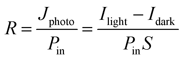
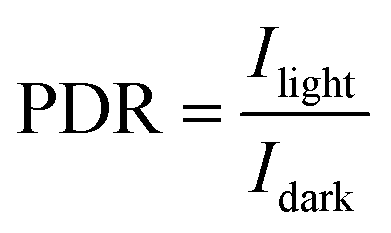
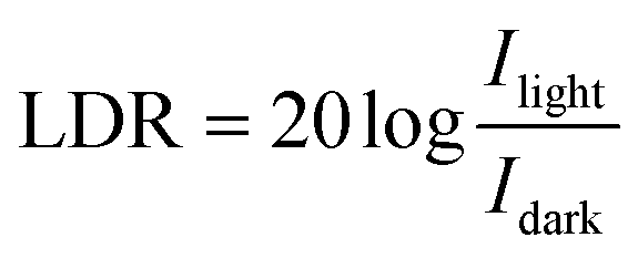
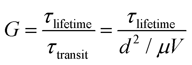
The evaluation of the performance of a photodetector requires many different parameters. The basic parameters include responsivity (R), linear dynamic range (LDR), detectivity (D*), on/off ration (PDR), external quantum efficiency (EQE), response time, photoconductive gain (G), and noise equivalent power (NEP). Here, we provide the definition and calculation formula for each parameter.where Jphoto is the photocurrent density, and Pin is the power density of the incident light. Ilight and Idark are the currents under light and dark conditions, respectively, and S is the effective area of the photodetector.
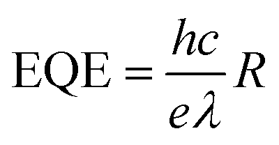
where h is Planck's constant (h = 6.626 × 10⁻³⁴J s), c is the speed of light (c = 3.0 × 10⁸m s−1), e is the elementary electron constant, and λ is the wavelength of the incident light.
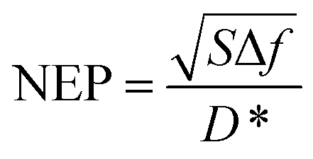
where Δf is the electrical bandwidth, and In is the noise current, which is mainly composed of three parts: dark-current-induced shot noise, Johnson–Nyquist noise, and thermal fluctuation “flicker” noise.3 When the noise current is dominated by dark current, D* can be simplified as follows:3
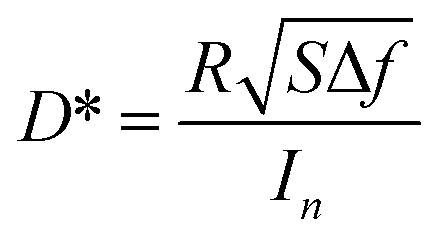
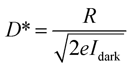
The higher the value of D*, the stronger the ability of the detector to detect weak signals. Therefore, to detect very weak optical signals, the dark current should be reduced as much as possible.
NEP is defined as the signal light power in which the signal-to-noise ratio is 1, indicating that the photodetector can distinguish the minimum excitation light power of the signal from the noise. It can be calculated by:
where Ilight is the photocurrent and Idark is the dark current.
where d is the thickness of the photodetector (for planar detectors, d is the distance between the two electrodes) length of photodetectors, V is the bias voltage, and μ is the carrier mobility.
3. Metal halide perovskite solar blind photodetector
MHP is a low-cost solution machinable material. Recently, it has been gradually introduced to study the solar blind photodetector owing to its excellent intrinsic characteristics, including its wide band gap adjustability, high carrier mobility, high light absorption coefficient, high emission colour purity (narrow maximum half width), and high photoluminescence quantum efficiency.29,30 Generally, MHP can be divided into 3D, 2D, 1D, and 0D structures, according to the crystal structural dimensionalities at the molecular level (Fig. 1). This means that the individual components forming the perovskite framework should show different dimensions at the molecular level. Specifically, according to the periodic spatial arrangement pattern of (BX6)4− octahedral units and their surrounding A-site cations, these low-dimensional perovskites composed of (BX6)4− octahedrons usually exist in the form of isolated octahedral flakes (2D), octahedral chains (1D) and octahedral clusters (0D).31 The different molecular structures achieve different photoelectric properties for the MHPs. Next, we will describe and discuss the solar blind DUVPDs based on MHPs from different dimensions (3D, 2D, 1D, 0D or QDs).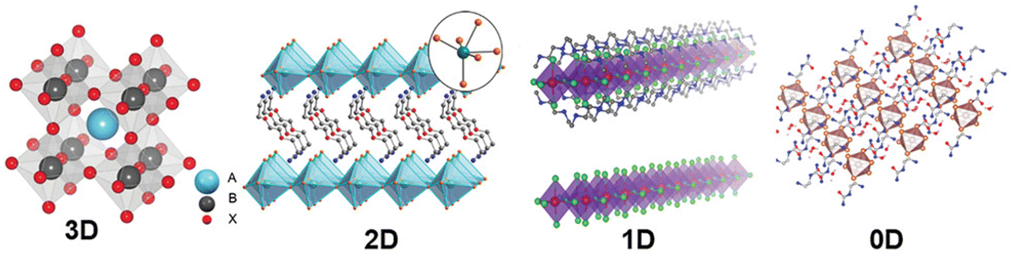 | ||
| Fig. 1 Schematic diagram of the atomic level structures of 0D-3D MHP.93 Copyright 2021, The Authors. Advanced Science published by Wiley-VCH GmbH. | ||
3.1. 3D MHP solar blind DUVPDs
Typical 3D MHPs with the ABX3 formula have been used in DUVPDs, including the Pb-based inorganic perovskite CsPbX3, and the organic–inorganic hybrid perovskite (OIHP) MAPbX3 and FAPbX3 (X = Cl−, Br−, I− and their mixtures). In the 3D network structure, the A cation is located at 8 corners, the metal cation B occupies the body centre, and the X anion is located at 6 surface centres. B2+ and the six X-ions form an octahedron [BX6]4−. Finally, the octahedron [BX6]4− forms a 3D frame by sharing corners, and the middle position of the eight octahedrons is occupied by cation A, in which each element has a proper valence state to meet the requirements of charge balance.31In 2018, Tong et al. prepared an indirect self-powered P–I–N type DUV photodetector with a high response time of 7.8/33.6 μs in the DUV region by coating the dual-phase (CsPbBr3–Cs4PbBr6) inorganic perovskite material on the back surface of the photodetector.32 As shown in Fig. 2a and b, the CsPbBr3–Cs4PbBr6 window layer captures and down-converts the incident DUV light. Then, the down-converted photons (green light) are transmitted to the MAPbI3 active-layer through the FTO thin film. At the same time, spiro-OMeTAD and TiO2 are used as the hole transport layer and electron transport layer to separate the generated electron–hole pairs, respectively. As can be clearly seen from Fig. 2c, the device without the inorganic perovskite layer can hardly detect the light in the solar blind area, while the device with a biphasic inorganic perovskite film shows a higher responsiveness in the solar blind area. Moreover, the responsivity of the device in the range of 400–800 nm is obviously reduced after adding the biphasic inorganic perovskite film.
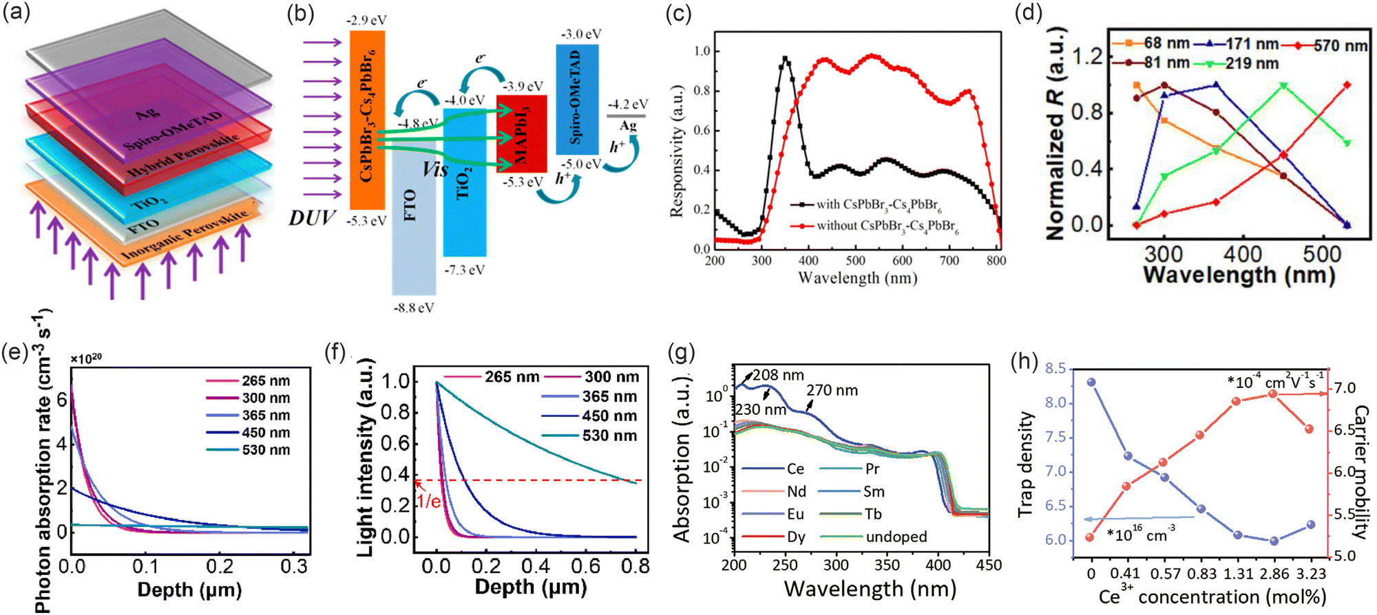 | ||
| Fig. 2 (a) Device structure. (b) Band gap diagram of the device without a window layer. (c) Responsivity spectra of the devices with/without the dual-phase inorganic perovskite film as a window layer.32 Copyright 2018, American Chemical Society. (d) Normalized optical response of CsPbBr3 nanosheet devices with different thicknesses. (e) Normalized attenuation curve of photon absorption with wavelength variation. (f) Normalized attenuation curves of incident light with different wavelengths.34 Copyright 2023, published by Elsevier Ltd on behalf of the editorial office of Journal of Materials Science & Technology. (g) Absorbance spectra of CsPbCl3 NCs doped with different rare earth ions. (h) Trap density and carrier mobility of perovskite NCs.36 Copyright 2021, Wiley-VCH GmbH. | ||
Another reason is that by changing the thickness, the light absorption of the perovskite semiconductors can be adjusted. For example, the peak response of the DUVPDs made of CsPbBr3 nanosheets with different thicknesses prepared by a simple solution-based confined space growth method at room temperature gradually shifts to blue with the decrease of thickness (Fig. 2d). When the thickness of the CsPbBr3 nanosheet is 68 nm, the blue shift of the peak response reaches 265 nm.34Fig. 2e shows that as the wavelength increases, the absorption rate of photons in the crystal decreases. Therefore, short-wavelength DUV light can be absorbed only with a very low penetration depth. The incident light of 265 nm only needs a penetration depth of about 20 nm (Fig. 2f). Finally, the photodetector made of 68 nm CsPbBr3 nanosheets has a response rate of 85 mA W−1 and a specific detection rate of 4.05 × 10¹¹ Jones under the illumination of 265 nm at 3 V.
Ion doping can adjust some properties of the perovskite, such as the carrier lifetime and interface defect density.35 Cerium ion shows a unique 4f–5d transition, and has a strong absorption band in the UV region.36 Doping a certain amount of Ce3+ into the CsPbCl3 nanocrystal (NC) can greatly improve the light absorption intensity of CsPbCl3 in the DUV region, reducing defects and improving the carrier mobility (Fig. 2g and h). Moreover, compared with CsPbCl3, the stability of CsPbCl3:Ce3+ in air is also improved.36 Subsequently, a DUV detector device based on plasma Al/CsPbCl3:Ce3+ hybrid film was prepared. Due to the plasma effect and Al-perovskite heterojunction, the absorption of the device is enhanced; thus, the photocurrent of the device is greatly improved. Finally, a high-performance DUV photoelectric detector is obtained, which has a very low dark current of 10−8 A, a high detection rate of 4 × 10¹³ Jones, and a short response time of 29 μs/52 μs at 230 nm.
The planar metal–semiconductor–metal (MSM) detectors based on MAPbX3 bulk crystals all show good performance under the illumination of 255 nm.42 The responsivities are 450 mA W−1 for MAPbCl3, 300 mA W−1 for MAPbBr3, and 120 mA W−1 for MAPbI3 at 5 V bias and 1.5 mW cm−2 255 nm light illumination, respectively. Although the responsivity and photocurrent of MAPbCl3-based detectors are better than those of MAPbBr3 and MAPbI3 under the same conditions, the response time of MAPbCl3-based detectors is longer (15/31 ms for MAPbCl3, 2.5/2.5 ms for MAPbBr3 and 2/2 ms for MAPbI3 at 10 V). The response time and carrier lifetime are correlated, and the trap state has the ability to increase the carrier lifetime. The longer response time of the MAPbCl3-based single crystal detector can be attributed to its higher density of trap state.
The separation of halide components occurs in the MAPbX3 perovskite due to its instability at high temperatures and greater sensitivity to light and moisture than the FAPbX3 perovskite. FAPbX3 exhibits good thermal stability. However, in humid environments, the black perovskite polymorph (α-phase), which remains stable above 160 °C, transforms into the yellow polymorph (δ-phase).43–45 It has been proved that the halide perovskite (with a combination of cationic and anionic components) can greatly increase the long-term stability of photodetector devices.46 Combining MAPbX3 with FAPbX3 can stabilize the perovskite phase of FAPbX3. The DUV photodetectors (Fig. 3a) based on (FAPbI3)1−x(MAPbBr3)x (x = 0, 0.03, 0.05, 0.07, 0.1) were prepared by adding MAPbBr3 to FAPbI3.47 While α-FAPbI3 rises in tandem with an increase in the MAPbBr3 content, the perovskite films' crystallinity does not always rise, but rather falls when it surpasses a particular threshold.48Fig. 3b and c show the light absorption and the responsivity (R) of the films under 254 nm radiation, respectively. Obviously, the device with x = 0.05 has higher light absorption and responsivity than other devices. Subsequently, the DUV detector with (FAPbI3)1−x(MAPbI3)x (x = 0.025, 0.05, 0.075 and 0.1) as the light absorption layer also shows good photoelectric performance, especially when x is 0.075, which further proves that the mixing of different cations can improve the photoelectric performance of the device to some extent (Fig. 3d and e).49
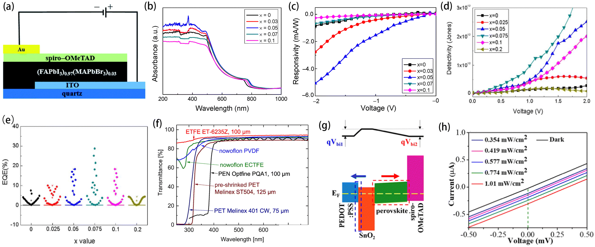 | ||
| Fig. 3 (a) Device structure based on the (FAPbI3)0.97(MAPbBr3)0.03 perovskite. (b) and (c) Light absorption and responsivity curves of the (FAPbI3)1−x(MAPbBr3)x films (x = 0, 0.03, 0.05, 0.07, and 0.01).47 Copyright 2022, by the authors. (d) and (e) Detectivity curves and EQE of PDs based on (FAPbI3)1−x (MAPbI3)x (x = 0.025, 0.05, 0.075 and 0.1).49 Copyright 2022, the Korean Ceramic Society. (f) Transmission spectra of common flexible polymers.94 Copyright 2016, Elsevier B.V. (g) Schematic diagram of the energy band arrangement of devices after contact. (h) I–V curves of under different light intensities and dark conditions.50 Copyright 2021, American Chemical Society. | ||
Flexible detectors are of great significance for the detection of some complex objects. However, the typical flexible polymer substrate strongly absorbs DUV light, which prevents DUV radiation from entering the active layer (Fig. 3f). Thi My Huyen Nguyen et al. developed a self-powered DUV detector using polyvinylidene fluoride (PVDF) as a flexible substrate.50Fig. 3g shows the band structure of the device. An interesting phenomenon is that two built-in potentials with opposite directions are formed in the device structure, and the amplitudes are almost the same, resulting in the I–V curve of the device being linear instead of rectifier characteristics (Fig. 3h). Moreover, the device's performance is significantly impacted by the control of the PVDF film thickness. A PVDF film that is excessively thin will naturally curl upon being peeled off from the bottom glass substrate. Conversely, a PVDF film that is too thick will reduce light transmittance throughout the entire spectral range. Furthermore, they made a wearable detector by rolling the prepared flexible detector into a circle and gluing it together with double-sided adhesive tape. The LED of the watch was used as the display for detecting deep ultraviolet light, showing its potential as a flexible wearable detector. However, one of the problems of this type of device is the low response rate, only 4.92 mA W−1 under the illumination of 254 nm at 0 V.
3.2. 2D MHP solar blind DUVPDs
Apart from conventional detection, polarized light detection is also an indispensable part of the field of solar blind detection. Polarization can be used to identify artificial objects in complex environments.51 So far, UV polarization detection has been applied in anti-counterfeiting, missile approach warnings, remote security monitoring and other practical equipment.52 As mentioned above, there is no solar blind radiation on the Earth's surface, and the solar blind DUVPD can achieve selective detection of UV light, while being insensitive to visible light. Such detectors are essential in many military and civilian applications for their high safety, high anti-interference capability, and low background noise.53 However, polarized light devices targeting the solar blind UV range are still scarce. Nevertheless, some emerging anisotropic 2D hybrid ferroelectric materials with relatively wide band gaps have been proven to be ideal candidate materials for solar blind polarized light detection due to their intrinsic anisotropic crystal structure and spontaneous polarization (Ps) characteristics.Using the 3D-to-2D dimension reduction strategy, Xu et al. designed a 2D multilayer mixed ferroelectric perovskite (EA)2(MA)2Pb3Cl10 (EA = CH3CH2NH3) with a band gap of 3.35 eV, and applied it to solar blind polarization detection for the first time.54Fig. 4a shows the crystal structure diagram of the (EA)2(MA)2Pb3Cl10 single crystal. MA+ cations are confined inside the cavities. As seen from Fig. 4b and c, the photocurrent and absorbance generated along the c-axis direction are much greater than those along the a-axis direction, whether under unpolarized light or polarized light at 266 nm. This confirms that due to the anisotropy of the crystal structure, different directions show different photoelectric properties. Fig. 4d shows the angle-resolved signal current of the detector, and it can be seen that the maximum photocurrent (Imax) appears at the polarization of 0° and 180°, corresponding to the polarization of light along the c-axis. When the polarization of light is parallel to the a-axis (defined as 90° and 270°), the photocurrent decreases to the minimum value (Imin). The polarization ratio ω (ω = Imax/Imin) represents the polarization detection ability of the detector. The polarization ratio of this polarization detector is 1.38, which is far lower than the polarization detector based on the 2D trilayered hybrid perovskite ferroelectric (allyammonium)2(ethylammonium)2Pb3Br10 (with a polarization ratio of 15).55 This is because the polarization ratio of the detector based on (EA)2(MA)2Pb3Cl10 is limited by the anisotropic absorption of the material, while (allyammonium)2(ethylammonium)2Pb3Br10 is driven by the bulk photovoltaic effect. Furthermore, its polarization ratio is independent of the absorption anisotropy of the material, but depends on the angle of light polarization, and therefore shows better polarization ratio. Fig. 4e shows that the signal current of the (EA)2(MA)2Pb3Cl10 detector is repeatable and periodic. All of these factors mean that (EA)2(MA)2Pb3Cl10 is a candidate material for solar blind polarized light detection.
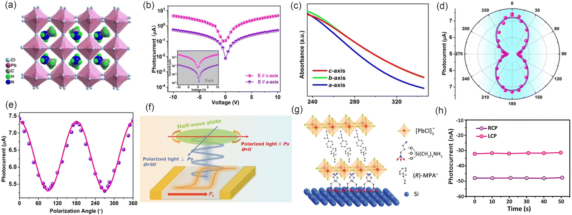 | ||
| Fig. 4 (a) Structure illumination of (EA)2(MA)2Pb3Cl10. (b) I–V curves measured along the c-axis and a-axis under an unpolarized light of 266 nm. (c) Optical absorbance along the three crystallographic axes. (d) Polar plot of the angle-resolved photocurrents.54 Copyright 2020, Wiley-VCH GmbH. (e) Polarization-dependent photocurrents. (f) Schematic illustration of the polarized-light device of (isobutylammonium)2(methylamium)Pb2Cl7.58 Copyright 2022, Wiley-VCH GmbH. (g) Structural illustration of the [(R)-MPA]2PbCl4/Si heterostructure. (h) Photocurrent of the device under RCP and LCP illumination.60 Copyright 2021, Wiley-VCH GmbH. | ||
Subsequently, researchers discovered some other 2D perovskite ferroelectric materials that can be used for solar blind detection. For example, EA4Pb3Cl10 synthesized by Wang et al. with a band gap of 3.39 eV shows self-powered DUV detection ability under 266 nm illumination.56 A photodetector based on 2D lead bromide mixed ferroelectric perovskite (C8H11FN)2PbBr4 (C8H10FN = 4-fluorophenylethylamine) has been proved to have a responsivity of 288 mA W−1 and a detection rate of 1.6 × 10¹¹ Jones under the illumination of 10 V at 254 nm.57 Lu et al. produced a self-powered polarization detector in the solar blind region by using the bulk photovoltaic effect (BPVE) induced by spontaneous polarization of 2D hybrid perovskite ferroelectrics as the driving source of self-supplied electro-optical detection.58 The schematic diagram of self-powered detection of polarized light in the UVC region under zero bias irradiation at 266 nm is shown in Fig. 4f. The angle (θ) between the Ps and the polarized light is adjusted by a half-wave plate. When the polarized light direction is parallel to the Ps direction, θ = 0°, the short-circuit current Isc is the largest. The minimum value (Imin) is reached at θ = 90° when polarized light is perpendicular to Ps. The polarization ratio is obtained up to 2.5, higher than that of (EA)2(MA)2Pb3Cl10 mentioned above.
Circular polarized light (CPL) detection is a small branch of polarized light detection, but so far, only one study has investigated CPL detection in the solar blind area. Due to structural asymmetry, chiral perovskites (their mirror image cannot coincide with it) are inherently sensitive to CPL.59 Thus, the study realized CPL detection in the solar blind area by growing wide band gap chiral perovskite [(R)-MPA]2PbCl4 ((R)-MPA = methylphenethylammonium) single crystals onto silicon wafers (Fig. 4g).60Fig. 4h shows that the detector can distinguish right-handed circularly polarized (RCP) and left-handed circularly polarized (LCP) well.
3.3. 1D MHP solar blind DUVPDs
1D MHPs usually have high crystal quality, a large surface-to-volume ratio, anisotropic geometry, low trap density, a long charge carrier lifetime, and a low carrier recombination rate.61 So far, however, the only 1D material used for solar blind detection is CsCu2I3. Fig. 5a and b show the crystal structure of 1D CsCu2I3, which belongs to the orthorhombic space group Cmcm. The framework contains one Cs site, one Cu site and two different types of I sites.62 The central octahedral (core), made up of copper and iodine atoms, is enclosed and separated by adjacent cesium atoms (shell), forming a distinctive core–shell structure. This arrangement results in a robust 1D local electron distribution and greater stability compared to the 0D Cs3Cu2I5.63 In addition to good stability, its wide band gap (usually higher than 3.7 eV) and non-toxicity are also important reasons why it can be used for solar blind detection.64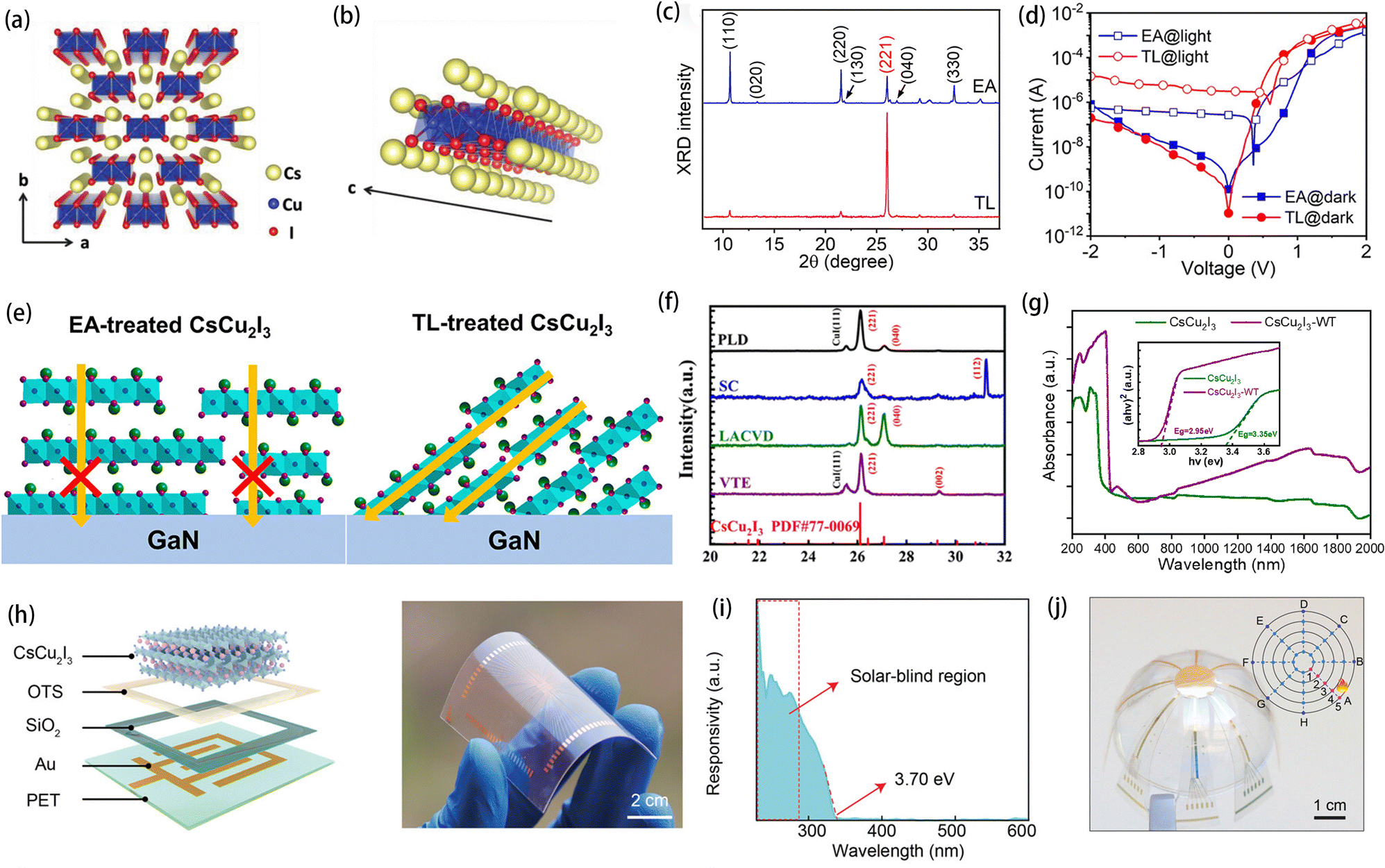 | ||
| Fig. 5 (a) Perspective view of the crystal structure along the [001] direction. (b) View of the 1D Cu(I) iodide wire surrounded by Cs atoms.62 Copyright 2020, WILEY-VCH Verlag GmbH & Co. KGaA, Weinheim. (c) XRD patterns of CsCu2I3 films with different antisolvents. (d) I–V curves of devices using EA and TL antisolvents in the dark and under a UV light intensity of 46 mW cm−2. (e) Schematic diagram of the exciton transport in CsCu2I3 films with different orientations of 1D [Cu2I3]− chains.66 Copyright 2022, American Chemical Society. (f) XRD patterns of the CsCu2I3 films prepared via VTE PLD, LACVD and SC.72 Copyright 2023, the Royal Society of Chemistry. (g) Absorbance curves and band gap (inset) of CsCu2I3 crystals before and after water treatment.95 Copyright 2022, Elsevier Ltd and Techna Group S.r.l. (h) Schematic diagram of the solar blind PD structure and optical image of the flexible solar blind PD array. (i) Response spectrum of the solar blind PDs array. (j) Optical diagram of the flame detection device. The illustration is the corresponding 2D plan.75 Copyright 2023, Wiley-VCH GmbH. | ||
The anti-solvent method is often used to synthesize CsCu2I3. Li et al. used diethyl ether as anti-solvent to synthesize CsCu2I3 nanowires, and successfully realized polarization-sensitive DUV detection.65 CsCu2I3 thin films grown with toluene (TL) as an antisolvent showed preferential (221) orientation, whereas films prepared with ethyl acetate (EA) as an antisolvent showed random orientation, which can be seen from the XRD pattern (Fig. 5c).66Fig. 5d shows the I–V curves of CsCu2I3/GaN heterojunction detectors treated with EA and TL under dark conditions and 275 nm irradiation. It can be seen that the TL detector has a smaller reverse saturation current and larger forward saturation current compared with the EA detector. This is because the EA antisolvent leads to the orientation of the film being mainly based on the (110) crystal plane. This makes the 1D [Cu2I3]− anion chain completely parallel to the substrate, and is not conducive to the diffusion/charge transport of excitons along the direction perpendicular to the substrate. On the contrary, the TL antisolvent makes the CsCu2I3 perovskite film grow with the preferential (221) orientation, and the 1D [Cu2I3]− anion chain crosses the substrate at an angle of 30° (Fig. 5e). This improves the exciton/charge transport, thus improving the response speed of the device.66
After the development of the CsCu2I3-based solar blind detector, researchers also sought some methods to improve the performance of copper-based solar blind detectors. One way is to control the dropping time of the antisolvent, which affects the crystal orientation and the size of the crystal boundary. Within a certain range, with the extension of the anti-solvent dripping time, the number of pinholes gradually decreases and the crystal size gradually increases. This occurs because introducing the anti-solvent at the right moment can enhance the evaporation of the residual solvent, leading to a noticeable supersaturation of the precursor solution.67 The corresponding detector has a cutoff wavelength of 303 nm, and is highly responsive to solar blind light. Furthermore, after being stored in ambient air for 2 months, it can retain nearly 95% of the initial photocurrent. By optimizing the annealing process, the crystallinity of the CsCu2I3 thin film also can be improved.68 Unlike the optimization of anti-solvent types and annealing temperature in previous literature,67–70 Li et al. added I2 to the synthesis process to change the growth kinetics, and obtained high quality pinhole-free CsCu2I3 thin films.71 Furthermore, a free-space optical communication system that can transmit characters under ambient light sources is successfully realized using the corresponding CsCu2I3 solar blind DUV detector modified by I2.
Besides the above methods, laser-assisted chemical vapor deposition (LACVD), pulsed laser deposition (PLD), vacuum thermal evaporation (VTE), and spin coating (SC) are also used to prepare CsCu2I3 thin films.72 The results show that all CsCu2I3 thin films grown on the GaN substrate have the (221) plane corresponding to CsCu2I3 (JCPDSNo. 77-0069), but the growth samples prepared by SC preferentially grow along the (112) plane (Fig. 5f). Furthermore, by testing and comparing the photoelectric properties of the CsCu2I3/n-GaN heterojunction UV PDs prepared by these four different methods, it is found that the R (42 mA W−1) and D (1.42 × 10¹¹ Jones) of the PD prepared by VTE is higher than those of other devices.
Different heterojunction structures generally have different spectral response ranges and intensities. The photodetector based on the CsCu2I3/Si heterojunction has high spectral selectivity. It exhibits high sensitivity to light within the wavelength range of 280–370 nm,64 while the heterojunction photodetector based on p-CuI/CsCu2I3/n-GaN has self-powered characteristics and shows responses in the UV band (300–400 nm).73 CsCu2I3 single crystal (SD) decomposition by water treatment (WT) results in the formation of a CsCu2I3/CuI heterojunction because CsI has a high solubility in water and CuI has a very low solubility. As can be seen from Fig. 5g, after water treatment, the band gap of the CsCu2I3 single crystal is reduced. However, the CuI nanoparticles attached to the surface of CsCu2I3 enhance the light capture, which improves the absorption efficiency of CsCu2I3-WT from UV, visible light to near infrared light. The responsivity of the photodetector based on the CsCu2I3/CuI heterojunction is 840 mA W−1 under the irradiation of 250 nm light, which is much higher than most other reported values (Table 1).
| Material and structure | Wavelength (nm) | Method | Voltage (V) | τ r/τf | R [mA W−1] | D [Jones] | Ref. |
|---|---|---|---|---|---|---|---|
| CsPbX3 QDs/a-Si radial PIN junction/glass | 200 | Solution | 0 | 0.48/1.03 ms | 54 | 33 | |
| CsPbBr3–Cs4PbBr6/FTO/TiO2/MAPbI3/spiro-OMeTAD/Ag | 254 | Vapor | 0 | 7.8/33.6 μs | 49.4 | 1.2 × 10¹² | 32 |
| CsPbBr3 QDs/CPI film/ITO glass/MAPbI3/Au | 279 | Solution | −0.1 | <70 ms | 1.4 | 2.4 × 10¹¹ | 87 |
| FTO glass/AI film/CsPbBr3 NCs/Au | 230 | Solution | 29/52 μs | 450 | 2.0 × 10¹² | 36 | |
| Si/SiO2/graphene-CsPbBr3/Cu | 266 | Solution | 22.8 A W−1 | 1.89 × 10¹⁰ | 96 | ||
| Glass/CsPbBr3 nanosheet/Au | 265 | Solution | 3 | 3.4/10.2 ms | 85 | 4.05 × 10¹¹ | 34 |
| Glass/ITO/CsPbI2Br/P3HT/HAT-CN/SHE | 255 | Solution | 56.2 | 2.86 × 10¹³ | 97 | ||
| CsPb2Br5 | 280 | Solution | 2.5 | 25.1 | 98 | ||
| MAPbCl3 | 255 | Solution | 5 | 450 | 42 | ||
| MAPbBr3 | 255 | Solution | 5 | 300 | 42 | ||
| MAPbI3 | 255 | Solution | 5 | 120 | 42 | ||
| MAPbI3/β-Ga2O3 | 254 | Solution | 0.11/0.45 s | 85 | 1.28 × 10¹¹ | 99 | |
| ITO/(FAPbI3)0.97(MAPbBr3)0.03/spiro-OMeTAD/Au | 254 | Solution | 0 | 46/47 ms | 52.68 | 4.65 × 10¹¹ | 41 |
| Ag/PVDF/PEDOT:PSS/SnO2/(FAPbI3)1−x(MAPbBr3)x/spiro-OMeTAD/Au | 254 | Solution | 0 | 82/64 ms | 4.92 | 7.57 × 10¹⁰ | 50 |
| Willow glass/PH1000/perovskite/spiro-OMeTAD/PEDOT:PSS | 254 | Solution | 0 | 45/46 ms | 100 | ||
| ITO/(FAPbI3)0.95(MAPbI3)0.05/ITO | 254 | Solution | −2 | 5.07 | 5.49 × 10¹¹ | 47 | |
| ITO/(FAPbI3)0.925(MAPbI3)0.075/ITO | 254 | Solution | 2 | 5.87 | 4.15 × 10¹² | 49 | |
| ITO/SnO2/(FA)x(MA)1−xPbI3/spiro-OMeTAD/Au | 254 | Solution | 2 | 50.8 | 4.47 × 10¹³ | 101 | |
| ITO/PH1000/SnO2/(FAPbCl3)1−x(MAPbCl3)x/spiro-OMeTAD/Au | 254 | Solution | 0 | 5.6 | 4.03 × 10¹¹ | 102 | |
| ITO/SnO2-SDBS/FAPb(I/Br)3/spiro-OMeTAD/Au | 254 | Solution | 2 | 43.8 | 3.56 × 10¹³ | 103 | |
| β-Ga2O3/CsCu2I3 | 254 | Anti-solvent assisted crystallization | 10 | 1.70/0.61 s@0 V | 20 | 107 | 70 |
| CsCu2I3/GaN | Anti-solvent assisted method | 0 | 47.63 | 2.58 × 10¹² | 66 | ||
| CsCu2I3/Si | 330 | Pulsed laser deposition | 0 | 7.1 | 2.6 × 10¹¹ | 64 | |
| p-CuI/CsCu2I3/n-GaN | 365 | Vacuum thermal evaporation | 0 | 8.8/0.32 s | 71.7 | 3.3 × 10¹² | 73 |
| CsCu2I3/CuI | 250 | Anti-solvent evaporation-assisted crystallization | 5 | 840 | 2.75 × 10¹⁰ | 95 | |
| ITO/NiOx/CsCu2I3/PCBM/Ag | 365 | Anti-solvent assisted method | 0 | 1.49/1.33 ms | 42 | 1.1 × 10¹¹ | 68 |
| ITO/CsCu2I3/ITO | 265 | Anti-solvent assisted method | 11.6/16.2 ms | 150 | 3.45 × 10¹¹ | 67 | |
| Sapphire/CsCu2I3/Cu | 275 | Anti-solvent assisted crystallization | 0.684/0.686 s | 1.74 × 10⁻³ | 71 | ||
| ITO−Cs3Cu2I5−ITO | 265 | Solution | 26.2/49.9 ms | 64.9 | 77 | ||
| Au/Cs3Cu2I5/Au | 265 | Solution | 5 | 465/897 μs | 1.78 × 10⁴ | 1.12 × 10¹² | 79 |
| ITO–Cs3Cu2I5–ITO | 275 | Nanosphere-lithography technique | 1660 | 2.48 × 10¹² | 82 | ||
| Au/Cs3Cu2I5/Au | 265 | Supersaturation controlled growth strategy | 4.25 | 34/45 ms | 1.58 × 10⁵ | 1.01 × 10¹⁰ | 81 |
| Cs3Cu2I5/n-Si | 280 | Pulsed-laser deposited | 70.8 | 9.44 × 10¹¹ | 84 | ||
| Cs3Cu2I5/β-Ga2O3 | 265 | Dual-source vapor codeposition | 37/45 ms | 2.4 × 10⁸ | 86 | ||
| Cs3Cu2I5/ZnO | 280 | Low-temperature solution | 0.43/0.46 s | 314 | 1.26 × 10¹¹ | 88 |
Flexible photodetection devices can be used in wearable and portable electronic products because of their small size, lightweight, and ability to bend, roll or stretch.28,74 Lu et al. fabricated CsCu2I3 perovskite thin film array devices (Fig. 5h) with controllable morphology and uniform size on flexible substrate PET by the vacuum heating-assisted drop casting patterning (VHADP) process. These devices have an obvious response to 200–280 nm solar blind DUV light (Fig. 5i).75 They realized the reconstruction of solar blind DUV images using these flexible PD arrays. Not only that, but the team further explored the flame detection and early warning system with weak light detection capability. A hemispherical PD array with a diameter of 6 cm was designed by simple origami method, and 40 pixels were evenly distributed on 8 arms (Fig. 5j). It is capable of detecting multiple flame signals within a wide-angle range of 0–180 degrees, and can pinpoint the location of the flame by giving the output current intensity.75
3.4 0D or QDs solar blind DUVPDs
MHPs of 0D or QDs are ideal candidates for photodetectors because they usually have large extinction coefficients and multi-exciton generation characteristics.61 However, to the best of our knowledge, the only molecular level 0D MHP applied in the field of solar blind detection is Cs3Cu2I5 at present, while the morphological 0D (QDs) MHP is concentrated on CsPbX3.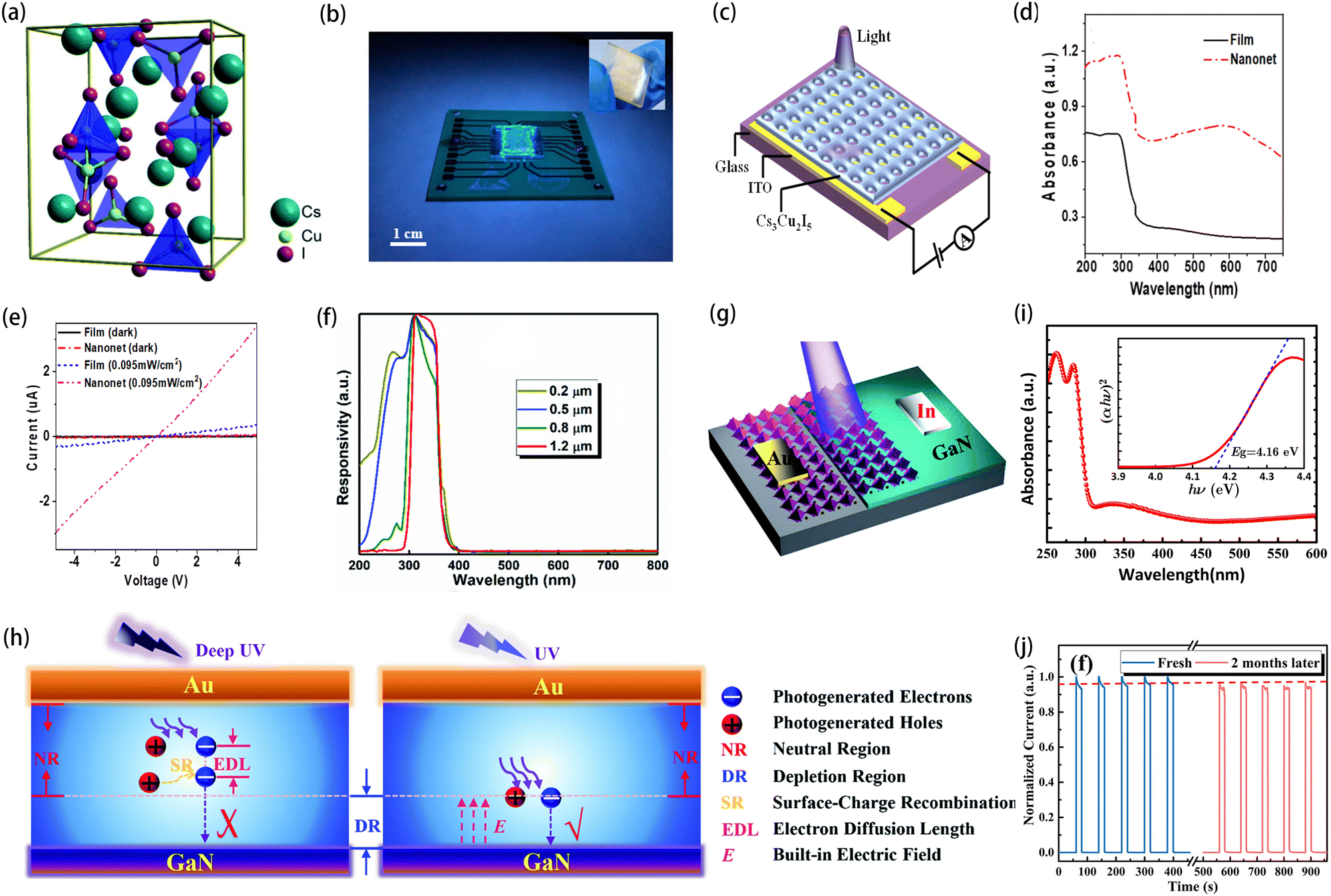 | ||
| Fig. 6 (a) Crystal structure of Cs3Cu2I5.83 Copyright 2020, the Royal Society of Chemistry. (b) Digital camera photograph of the DUV photodetector irradiated by 265 nm light. (Inset) DUV photodetector under white light.77 Copyright 2019, American Chemical Society. (c) Schematic diagram of DUV detection based on nano-hollow Cs3Cu2I5. (d) Absorption curves of the Cs3Cu2I5 thin film and nanonet. (e) I–V curves of the Cs3Cu2I5 nanonet and film photodetector under 275 nm irradiation with 0.095 mW cm−2 and in the dark.82 Copyright 2022, by the authors. Licensee MDPI, Basel, Switzerland. (f) Response spectra of the photodetector with different absorber thicknesses. (g) Schematic illustration of the Cs3Cu2I5/GaN heterojunction device. (h) Schematic diagram of the work mechanism.83 Copyright 2020, the Royal Society of Chemistry. (i) Absorption spectrum and the corresponding optical band gap (inset) of the Cs3Cu2I5 thin films deposited at 110 °C.84 Copyright 2021, Optical Society of America. (j) Stability evaluation of the photodetector after 2 months of storage in open air.86 Copyright 2021, American Chemical Society. | ||
The crystal structure, grain size, grain boundary, defect states, and other factors greatly influence the photoelectric properties of MHPs. The polycrystalline thin films of Cs3Cu2I5 produced through spin coating and thermal evaporation processes frequently exhibit numerous defect states and grain boundaries. These factors not only amplify the nonradiative recombination of charge carriers and diminish the photoresponsivity of detectors, but also compromise the material stability, thereby significantly impacting the operational lifespan of the devices.81 In order to avoid these features as much as possible, Xu et al. prepared uniform and ordered Cs3Cu2I5 nano-arrays (Fig. 6c) on a monolayer colloidal crystal (MCC) template made of 1 μm polystyrene (PS) balls using the nanosphere-lithography technique.82 As can be seen from Fig. 6d, the hollow nanonet array structure shows a stronger absorption rate than the dense spin-coated film. This result may be attributed to the enhanced light scattering and larger area in the pores of the nanonet structure, which makes the nanonet have much higher absorption efficiency than the dense film.82 Therefore, the photocurrent of the detector based on the nano-mesh structure is obviously higher than that of the traditional planar perovskite detector (Fig. 6e).
Different heterojunctions will affect the photoelectric properties of the device. The thickness of the thin film used to form the heterojunction can affect the spectral response of the photodetector (Fig. 6f). This can be explained as follows. Fig. 6g shows a Cs3Cu2I5/GaN heterojunction self-powered DUV detector. As shown in Fig. 6h, the photoactive layer (Cs3Cu2I5) of the photodetector can be partitioned into two distinct regions: the depletion region (DR) located adjacent to the GaN layer, and the outer neutral region (NR) in proximity to the Au electrode. Due to strong light absorption and limited electron diffusion length (EDL), DUV photons are destroyed by surface charge recombination before reaching the DR. Therefore, the carriers generated by light cannot reach DR and cannot contribute a photocurrent, which makes the photodetector have high spectral selectivity.83
The pulsed laser deposition (PLD) dual-source vapor codeposition technique (DSVCT) can accurately control the thickness and growth process of thin films. The high-quality Cs3Cu2I5 thin film deposited on a Si wafer by PLD even has a wide band gap of 4.16 eV (Fig. 6i).84 The corresponding Cs3Cu2I5/n-Si heterojunction DUV photodetector has a peak R of 70.8 mA W−1 and a specific D of 9.44 × 10¹¹ Jones under the irradiation of 280 nm. The Cs3Cu2Br5/n-GaN heterojunction self-powered DUV photodetector, which also uses PLD technology, shows obvious responses in the ultraviolet region of 270 nm and the corresponding D is 5.29 × 10¹¹ Jones.85 The Cs3Cu2I5/β-Ga2O3 heterojunction DUV detector prepared by DSVCT and optimized annealing shows excellent storage stability and high water and oxygen degradation tolerance.86 Even after being stored in ambient air for 2 months, the unpackaged devices can maintain almost the same photocurrent (Fig. 6j).
![[thin space (1/6-em)]](https://www.rsc.org/images/entities/char_2009.gif) :2) QDs as a down-conversion material with radial junction structures of silicon nanowires (SiNWs).33Fig. 7a shows the inorganic CsPbX3 QDs solution in cyclohexane under sunlight and UV light irradiation, and the structural diagram of the device. CsPbX3 QDs are coated onto the radial junction (RJ) of SiNWs by spin coating (Fig. 7b). When there is no CsPbX3 QDs coating, the incident UV photons (<320 nm) are completely absorbed and shielded by ITO with extremely low external light transmittance (Fig. 7c) and N-doped a-Si:H window layer. The incident UV signal has little chance to reach the i-layer in the radial PIN junction. When the CsPbX3 QDs coating is present, the incident solar blind DUV light is first absorbed by the CsPbX3 QDs coating and converted into visible light, and then absorbed by the photoactive i-layer in the radial PIN junction. Furthermore, when compared with the lateral configuration under the same conditions, the RJ photodetector shows better light absorption ability and responsiveness (Fig. 7d), because the enhanced light capture effect reduces the reflection loss (Fig. 7e). Finally, without any external power supply, the RJ photodetector's rise/fall time is 0.48/1.03 ms, and the peak response rate is 54 mA W−1 at 200 nm.
:2) QDs as a down-conversion material with radial junction structures of silicon nanowires (SiNWs).33Fig. 7a shows the inorganic CsPbX3 QDs solution in cyclohexane under sunlight and UV light irradiation, and the structural diagram of the device. CsPbX3 QDs are coated onto the radial junction (RJ) of SiNWs by spin coating (Fig. 7b). When there is no CsPbX3 QDs coating, the incident UV photons (<320 nm) are completely absorbed and shielded by ITO with extremely low external light transmittance (Fig. 7c) and N-doped a-Si:H window layer. The incident UV signal has little chance to reach the i-layer in the radial PIN junction. When the CsPbX3 QDs coating is present, the incident solar blind DUV light is first absorbed by the CsPbX3 QDs coating and converted into visible light, and then absorbed by the photoactive i-layer in the radial PIN junction. Furthermore, when compared with the lateral configuration under the same conditions, the RJ photodetector shows better light absorption ability and responsiveness (Fig. 7d), because the enhanced light capture effect reduces the reflection loss (Fig. 7e). Finally, without any external power supply, the RJ photodetector's rise/fall time is 0.48/1.03 ms, and the peak response rate is 54 mA W−1 at 200 nm.
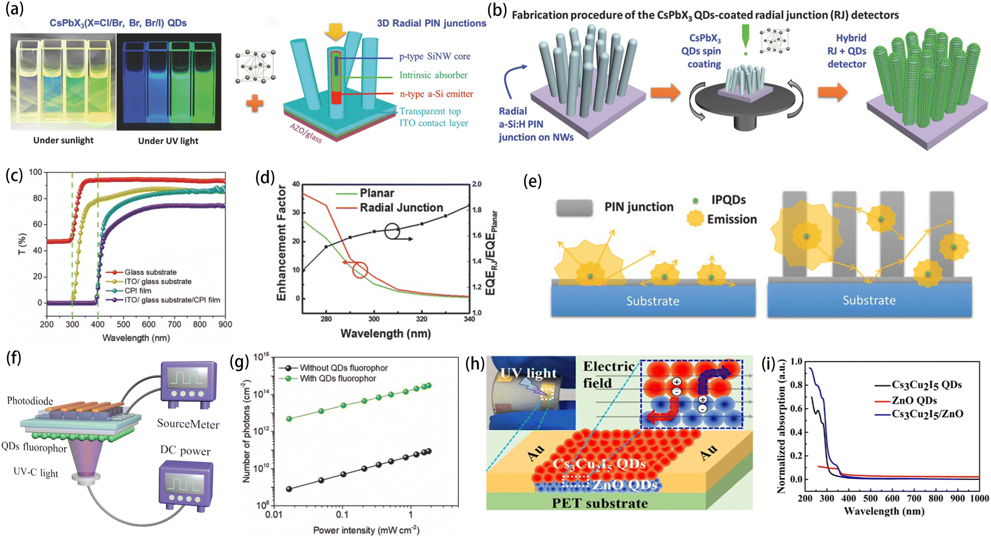 | ||
| Fig. 7 (a) Photographs of the solutions of inorganic CsPbX3 QDs in cyclohexane under sunlight and ultraviolet light irradiation, and the schematic diagram of the multilayer a-Si thin film PIN radial junction structure constructed on SiNWs. (b) Illustration of the spin-coating CsPbX3 QD thin film on a 3D SiNW radial junction architecture.33 (c) Optical transmission spectra of different substrates and films.87 (d) The wavelength-dependent EQE enhancement of the RJ and the planar junctions. (e) Different optical utilization properties of re-emitted and down-converted photons from IPQDs in RJ and planar structures.33 Copyright 2017, WILEY-VCH Verlag GmbH & Co. KGaA, Weinheim. (f) Schematic diagram of the integrated photoelectric detection system composed of a photodiode array and CsPbBr3 QDs. (g) The calculated number of photons reaching the perovskite surface with and without QD phosphors.87 Copyright 2019, WILEY-VCH Verlag GmbH & Co. KGaA, Weinheim. (h) Optical photographs and structural schematic diagram of the Cs3Cu2I5/ZnO heterostructure photodetector. (i) Absorption spectra of Cs3Cu2I5 QDs, ZnO QDs, and Cs3Cu2I5/ZnO.88 Copyright 2022, American Chemical Society. | ||
Similarly, Zou et al. cast CsPbBr3 QDs onto a colourless polyimide (CPI) film as a UV down-conversion layer, and combined it with a MAPbI3-based photodiode to form a photodetector array detection system (Fig. 7f).87 As can be seen from Fig. 7g, the number of corresponding photons reaching the perovskite layer after optical conversion is obviously increased. Under the illumination of 279 nm, the D of the device with and without CsPbBr3 QDs layer is 2.4 × 10¹¹ Jones and 3.7 × 10¹⁰ Jones, respectively. Zhao et al. constructed a flexible photodetector with a heterostructure of Cs3Cu2I5 QDs/ZnO QDs on the flexible substrate of PET by using the low-temperature solution combined with spin coating technology.88 The optical photographs and structural schematic diagram of the Cs3Cu2I5/ZnO heterostructure photodetector are shown in Fig. 7h. Fig. 7i shows the absorption curves of Cs3Cu2I5 QDs, ZnO QDs and Cs3Cu2I5/ZnO. It can be seen that the combination of Cs3Cu2I5 QDs and ZnO QDs enhances the absorption of Cs3Cu2I5/ZnO in the region of 200–280 nm. However, the response time (rise time 430 ms, fall time 460 ms) of this device is significantly higher than that of other heterojunction devices.
Conclusions and outlook
In this review, we comprehensively introduce and discuss the latest progress of MHP as a down-conversion material, and as the active layer of solar blind direct conversion detector. Specifically, it involves the synthesis method (mainly solution method), photoelectric properties and device properties of various forms of halide perovskite materials (namely 3D, 2D, 1D, 0D and QDs) with different chemical compositions and sizes based on Pb and Cu. The different proportions of copper and halide elements, coupled with the multiple coordination modes possible between them, and the various available inorganic and organic modules of the A-site result in a diversity of copper-based halide perovskites.89 However, from the above, we can see that among many copper-based halide perovskites, only Cs3Cu2I5 and CsCu2I3 are used as solar blind detection materials, and the application of many materials in this field has not been explored. In addition, we found that some zero-dimensional perovskites, such as Cs4SnCl6 and Cs4SnBr6, can have an energy bandgap above 3.9 eV.90,91 The reported metal-free perovskite PAZE-NH4X3·H2O (PAZE = piperazinium, C4N2H12) also has a bandgap of more than 4 eV.92 These other systems may be suitable for solar blind DUV photoelectric detection besides the copper halide system.In conclusion, solution-treatable low-cost halide perovskite has obvious advantages for solar blind DUV detection. Moreover, it can be used as a down-conversion material to convert solar blind light into visible light for indirect detection. However, there is still a lot of room for developing MHP solar blind detectors, such as flexible solar blind detection, polarized solar blind detection and others. Table 1 summarizes the main performances of MHP solar blind detectors in recent years. It is not difficult to draw a conclusion that MHP faces great opportunities and many challenges in the field of solar blind DUV detection, which are summarized as follows:
Opportunity
Challenge
Possible solutions
Author contributions
W. Yang conducted a literature survey and wrote the whole article. Y. Lei guided the writing process and writing ideas, and revised the article. Z. Jin guided and revised the whole project.Conflicts of interest
The authors declare no competing financial interests.Acknowledgements
This work was funded by the National Natural Science Foundation of China (22279049 and 52372287), the Fundamental Research Funds for the Central Universities (lzujbky-2023-eyt03 and 2023-it18), and the Natural Science Foundation of Gansu Province (23JRRA1017 and 23JRRA1160).References
- X. Hou, Y. Zou, M. Ding, Y. Qin, Z. Zhang, X. Ma, P. Tan, S. Yu, X. Zhou, X. Zhao, G. Xu, H. Sun and S. Long, J. Phys. D: Appl. Phys., 2020, 54, 043001 CrossRef
.
- L. Sang, M. Liao and M. Sumiya, Sensors, 2013, 13, 10482–10518 CrossRef CAS PubMed
- X. Chen, F. Ren, S. Gu and J. Ye, Photonics Res., 2019, 7, 381–415 CrossRef CAS
- S. H. Lee, S. B. Kim, Y.-J. Moon, S. M. Kim, H. J. Jung, M. S. Seo, K. M. Lee, S.-K. Kim and S. W. Lee, ACS Photonics, 2017, 4, 2937–2943 CrossRef CAS
- X. Hou, X. Zhao, Y. Zhang, Z. Zhang, Y. Liu, Y. Qin, P. Tan, C. Chen, S. Yu, M. Ding, G. Xu, Q. Hu and S. Long, Adv. Mater., 2021, 34, 2106923 CrossRef PubMed
- C. N. Lin, Y. J. Lu, X. Yang, Y. Z. Tian, C. J. Gao, J. L. Sun, L. Dong, F. Zhong, W. D. Hu and C. X. Shan, Adv. Opt. Mater., 2018, 6, 1800068 CrossRef
- M. Qiu, Z. Jia, M. Yang, K. Nishimura, C.-T. Lin, N. Jiang and Q. Yuan, Nanotechnology, 2023, 34, 285204 CrossRef PubMed
- Z. Li, D. Zhou, W. Xu, F. Ren, R. Zhang, Y. Zheng and H. Lu, IEEE Photonics Technol. Lett., 2022, 34, 935–938 CAS
- Y.-C. Chen, Y.-J. Lu, Q. Liu, C.-N. Lin, J. Guo, J.-H. Zang, Y.-Z. Tian and C.-X. Shan, J. Mater. Chem. C, 2019, 7, 2557–2562 RSC
- Y. Zhou, Z. Zhang, X. Yang, T. Liu, G. He, C. Lin, W.-T. Huang, H. Liu, Y. Wang, Y. Wang, Z. Xiang and C.-X. Shan, ACS Nano, 2024, 18, 7610–7617 CrossRef CAS PubMed
- H. Sheoran, S. Fang, F. Liang, Z. Huang, S. Kaushik, N. Manikanthababu, X. Zhao, H. Sun, R. Singh and S. Long, ACS Appl. Mater. Interfaces, 2022, 14, 52096–52107 CrossRef CAS PubMed
- A. S. Pratiyush, Z. Xia, S. Kumar, Y. Zhang, C. Joishi, R. Muralidharan, S. Rajan and D. N. Nath, IEEE Photonics Technol. Lett., 2018, 30, 2025–2028 CAS
- P. Xing, D. Ma, K. J. A. Ooi, J. W. Choi, A. M. Agarwal and D. Tan, ACS Photonics, 2019, 6, 1162–1167 CrossRef CAS
- H. Jia, R. Zhang, X. Niu, X. Zhang, H. Zhou, X. Liu, Z. Fang, F. Chang, B. O. Guan and J. Qiu, Adv. Sci., 2024, 11, 2309433 CrossRef CAS PubMed
- X.-K. Liu, W. Xu, S. Bai, Y. Jin, J. Wang, R. H. Friend and F. Gao, Nat. Mater., 2020, 20, 10–21 CrossRef PubMed
- L. Sun, W. Li, W. Zhu and Z. Chen, J. Mater. Chem. C, 2020, 8, 11664–11674 RSC
- Y. Zhang, M. Lyu, T. Qiu, E. Han, I. K. Kim, M.-C. Jung, Y. H. Ng, J.-H. Yun and L. Wang, Energies, 2020, 13, 4250 CrossRef CAS
- X. Guan, T. Wan, L. Hu, C. H. Lin, J. Yang, J. K. Huang, C. Y. Huang, S. Shahrokhi, A. Younis, K. Ramadass, K. Liu, A. Vinu, J. Yi, D. Chu and T. Wu, Adv. Funct. Mater., 2022, 32, 2110975 CrossRef CAS
- G. Vescio, J. Sanchez-Diaz, J. L. Frieiro, R. S. Sánchez, S. Hernández, A. Cirera, I. Mora-Seró and B. Garrido, ACS Energy Lett., 2022, 7, 3653–3655 CrossRef CAS PubMed
- L. Li, H. Chen, Z. Fang, X. Meng, C. Zuo, M. Lv, Y. Tian, Y. Fang, Z. Xiao, C. Shan, Z. Xiao, Z. Jin, G. Shen, L. Shen and L. Ding, Adv. Mater., 2020, 32, 1907257 CrossRef CAS PubMed
- Y. Xu, Z. Li, T. Yu, G. Peng, Y. Lei, H. Chen, Y. Wu, H. Wang and Z. Jin, Laser Photonics Rev., 2023, 18, 2300654 CrossRef
- H. Yao, Z. Li, C. Shi, Y. Xu, Q. Wang, Z. Li, G. Peng, Y. Lei, H. Wang, Z. Ci and Z. Jin, Adv. Funct. Mater., 2022, 32, 2205029 CrossRef CAS
- W. Fang, Q. Li, J. Li, Y. Li, Q. Zhang, R. Chen, M. Wang, F. Yun and T. Wang, Crystals, 2023, 13, 915 CrossRef CAS
- D. Li, T. Zhu, Y. Wu, P. Chen, S. Jiao, Z. Tang, Z. Gao, X. Sun, Z. Yang, H.-L. Cai and X. Wu, J. Phys. Chem. C, 2023, 127, 13478–13483 CrossRef CAS
- H. Jia, J. Chen, Q. Li, D. Li, Z. Liu, J. Zhao, C. Ding, W. Zhang, H. Yang, L. Pan, X. Feng, Z. Chen, X. Liu and J. Qiu, Phys. Status Solidi A, 2018, 216, 1800572 CrossRef
- X. Zhang, X. Liu, Y. Huang, B. Sun, Z. Liu, G. Liao and T. Shi, Front. Mech. Eng., 2023, 18, 33 CrossRef
- C. Bao, Z. Chen, Y. Fang, H. Wei, Y. Deng, X. Xiao, L. Li and J. Huang, Adv. Mater., 2017, 29, 1703209 CrossRef PubMed
- T. M. H. Nguyen, S. G. Shin, H. W. Choi and C. W. Bark, Exploration, 2022, 2, 20210078 CrossRef PubMed
- S. Adjokatse, H.-H. Fang and M. A. Loi, Mater. Today, 2017, 20, 413–424 CrossRef CAS
- J. Zhang, Q. Wang, X. Zhang, J. Jiang, Z. Gao, Z. Jin and S. Liu, RSC Adv., 2017, 7, 36722–36727 RSC
- Z. Chu, X. Chu, Y. Zhao, Q. Ye, J. Jiang, X. Zhang and J. You, Small Struct., 2021, 2, 2000133 CrossRef CAS
- G. Tong, H. Li, Z. Zhu, Y. Zhang, L. Yu, J. Xu and Y. Jiang, J. Phys. Chem. Lett., 2018, 9, 1592–1599 CrossRef CAS PubMed
- J. Lu, X. Sheng, G. Tong, Z. Yu, X. Sun, L. Yu, X. Xu, J. Wang, J. Xu, Y. Shi and K. Chen, Adv. Mater., 2017, 29, 1700400 CrossRef PubMed
- C.-Y. Wu, Y.-X. Le, L.-Y. Liang, J.-Y. Li, F.-X. Liang, S.-R. Chen, X.-P. Yang, Y.-X. Zhou and L.-B. Luo, J. Mater. Sci. Technol., 2023, 159, 251–257 CrossRef CAS
- Y. Lei, Y. Xu, M. Wang, G. Zhu and Z. Jin, Small, 2021, 17, 2005495 CrossRef CAS PubMed
- D. Li, W. Xu, D. Zhou, Y. Ji, N. Ding, X. Chen, J. Zhu, R. Sun, S. Lu, C. Ma, Z. Jia, G. Qin, X. Bai and H. Song, Adv. Opt. Mater., 2021, 9, 2100423 CrossRef CAS
- W. Zhu, S. Wang, X. Zhang, A. Wang, C. Wu and F. Hao, Small, 2022, 18, 2105783 CrossRef CAS PubMed
- A. Kumar, D. W. Chang and J.-B. Baek, Energy Fuels, 2023, 37, 17782–17802 CrossRef CAS
- Z. Chen, C. Li, A. A. Zhumekenov, X. Zheng, C. Yang, H. Yang, Y. He, B. Turedi, O. F. Mohammed, L. Shen and O. M. Bakr, Adv. Opt. Mater., 2019, 7, 1900506 CrossRef CAS
- Y. Guo, C. Liu, H. Tanaka and E. Nakamura, J. Phys. Chem. Lett., 2015, 6, 535–539 CrossRef CAS PubMed
- T. M. H. Nguyen, S. Kim and C. W. Bark, J. Mater. Chem. A, 2021, 9, 1269–1276 RSC
- Z. Zhang, W. Zheng, R. Lin and F. Huang, R. Soc. Open Sci., 2018, 5, 180905 CrossRef PubMed
- N. J. Jeon, J. H. Noh, W. S. Yang, Y. C. Kim, S. Ryu, J. Seo and S. I. Seok, Nature, 2015, 517, 476–480 CrossRef CAS PubMed
- Y. Reyna, M. Salado, S. Kazim, A. Pérez-Tomas, S. Ahmad and M. Lira-Cantu, Nano Energy, 2016, 30, 570–579 CrossRef CAS
- T. T. Ava, A. Al Mamun, S. Marsillac and G. Namkoong, Appl. Sci., 2019, 9, 188 CrossRef CAS
- H. Gong, Q. Song, C. Ji, H. Zhang, C. Liang, F. Sun, C. Zhang, A. Yang, D. Li, X. Jing, F. You and Z. He, J. Mater. Chem.
A, 2022, 10, 2876–2887 RSC
- G. I. Choi and H. W. Choi, Nanomaterials, 2022, 12, 1132 CrossRef CAS PubMed
- G. Wu, J. Zhou, R. Meng, B. Xue, H. Zhou, Z. Tang and Y. Zhang, Phys. Chem. Chem. Phys., 2019, 21, 3106–3113 RSC
- G. I. Choi and H. W. Choi, J. Korean Ceram. Soc., 2022, 60, 90–98 CrossRef
- T. M. H. Nguyen, S. K. Lee, S. Kim and C. W. Bark, ACS Appl. Mater. Interfaces, 2021, 13, 57609–57618 CrossRef CAS PubMed
- Y. Ge, M. Zhang, L. Wang, L. Meng, J. Tang, Y. Chen, L. Wang and H. Zhong, Adv. Opt. Mater., 2019, 7, 1900330 CrossRef
- J. Wang, C. Jiang, W. Li and X. Xiao, Adv. Opt. Mater., 2022, 10, 2102436 CrossRef CAS
- C. Xie, X. T. Lu, X. W. Tong, Z. X. Zhang, F. X. Liang, L. Liang, L. B. Luo and Y. C. Wu, Adv. Funct. Mater., 2019, 29, 1806006 CrossRef
- Z. Xu, W. Weng, Y. Li, X. Liu, T. Yang, M. Li, X. Huang, J. Luo and Z. Sun, Angew. Chem., Int. Ed., 2020, 59, 21693–21697 CrossRef CAS PubMed
- Y. Peng, X. Liu, Z. Sun, C. Ji, L. Li, Z. Wu, S. Wang, Y. Yao, M. Hong and J. Luo, Angew. Chem., Int. Ed., 2020, 59, 3933–3937 CrossRef CAS PubMed
- S. Wang, L. Li, W. Weng, C. Ji, X. Liu, Z. Sun, W. Lin, M. Hong and J. Luo, J. Am. Chem. Soc., 2019, 142, 55–59 CrossRef PubMed
- Y. Wang, B. Su, G. Lin, H. Lou, S. Wang, C.-Y. Yue and X. Lei, CrystEngComm, 2022, 24, 2258–2263 RSC
- L. Lu, W. Weng, Y. Ma, Y. Liu, S. Han, X. Liu, H. Xu, W. Lin, Z. Sun and J. Luo, Angew. Chem., Int. Ed., 2022, 61, e202205030 CrossRef CAS PubMed
- G. Long, R. Sabatini, M. I. Saidaminov, G. Lakhwani, A. Rasmita, X. Liu, E. H. Sargent and W. Gao, Nat. Rev. Mater., 2020, 5, 423–439 CrossRef
- X. Zhang, W. Weng, L. Li, H. Wu, Y. Yao, Z. Wang, X. Liu, W. Lin and J. Luo, Small, 2021, 17, 2102884 CrossRef CAS PubMed
- Y. Wang, L. Song, Y. Chen and W. Huang, ACS Photonics, 2019, 7, 10–28 CrossRef
- Z. Li, Z. Li, Z. Shi and X. Fang, Adv. Funct. Mater., 2020, 30, 2002634 CrossRef CAS
- R. Lin, Q. Guo, Q. Zhu, Y. Zhu, W. Zheng and F. Huang, Adv. Mater., 2019, 31, 1905079 CrossRef CAS PubMed
- C. Wang, F. Zhao, Z. Zhou, X. Li, S. He, M. Zhang, D. Zhang and L. Zhang, J. Alloys Comp., 2022, 905, 164245 CrossRef CAS
- Y. Li, Z. Shi, L. Wang, Y. Chen, W. Liang, D. Wu, X. Li, Y. Zhang, C. Shan and X. Fang, Mater. Horiz., 2020, 7, 1613–1622 RSC
- M. Li, C. Cao, W. Liu, N. Wang, C. Yi, R. Li and J. Wang, J. Phys. Chem. Lett., 2022, 13, 6462–6467 CrossRef CAS PubMed
- J. Pan, L. Mao, Z. Gao, J. Han, Y. Huang, Y. Wei, C. Lin, S. Yan, C. Liu, F. Fang, X. Zhao, B. Wang, X. Liu, Z. Tao, J. Zhao, J. Xu, Z. Li, J. Chen, J. Chang and L. Wang, IEEE Electron Device Lett., 2023, 44, 1660–1663 CAS
- J. Zou, J. Liu, X. Wang, Z. Han, Y. Gu, Z. He, X. Lu, X. Xu and Y. Zou, ACS Appl. Electron. Mater., 2023, 5, 2829–2837 CrossRef CAS
- J. Yang, W. Kang, Z. Liu, M. Pi, L.-B. Luo, C. Li, H. Lin, Z. Luo, J. Du, M. Zhou and X. Tang, J. Phys. Chem. Lett., 2020, 11, 6880–6886 CrossRef CAS PubMed
- A. Gao, W. Jiang, G. Ma, Z. Liu, S. Li, Z. Yan, W. Sun, S. Zhang and W. Tang, Curr. Appl. Phys., 2022, 33, 20–26 CrossRef
- C.-X. Li, S.-B. Cho, S.-H. Sohn and I.-K. Park, J. Alloys Comp., 2024, 973, 172925 CrossRef CAS
- X. Li, B. Xia, L. Zhang, F. Wang and F. Zhao, J. Mater. Chem. C, 2023, 11, 10215–10220 RSC
- X. Zhou, C. Wang, J. Luo, L. Zhang, F. Zhao and Q. Ke, Chem. Eng. J., 2022, 450, 136364 CrossRef CAS
- S. Wang, Y. Lei, H. Chen, G. Peng, Q. Wang, H. Wang, J. Duan and Z. Jin, Small, 2022, 18, 2205095 CrossRef CAS PubMed
- Q. Lu, Y. Zhang, G. Yang, M. Xiong, W. Wu, Z. Xu, H. Lu, Y. Liang, Z. He, Y. Yu, X. Mo, X. Han and C. Pan, Small, 2023, 19, 2300364 CrossRef CAS PubMed
- F. Qiu, G. Peng, Y. Xu, H. Wang and Z. Jin, Adv. Funct. Mater., 2023, 33, 2303417 CrossRef CAS
- Z.-X. Zhang, C. Li, Y. Lu, X.-W. Tong, F.-X. Liang, X.-Y. Zhao, D. Wu, C. Xie and L.-B. Luo, J. Phys. Chem. Lett., 2019, 10, 5343–5350 CrossRef CAS PubMed
- F. Qiu, Y. Lei and Z. Jin, Front. Optoelectron., 2022, 15, 47 CrossRef PubMed
- W.-Q. Liang, Y. Li, J.-L. Ma, Y. Wang, J.-J. Yan, X. Chen, D. Wu, Y.-T. Tian, X.-J. Li and Z.-F. Shi, Nanoscale, 2020, 12, 17213–17221 RSC
- F. Zeng, Y. Guo, W. Hu, Y. Tan, X. Zhang, J. Feng and X. Tang, ACS Appl. Mater. Interfaces, 2020, 12, 23094–23101 CrossRef CAS PubMed
- J. Ma, M. Zhang, H. Jiang, X. Chen, W. Di, X. Li, Y. Zhang, C. Shan and Z. Shi, Nano Today, 2023, 52, 101970 CrossRef CAS
- S. Xu, J. Tang, J. Qu, P. Xia, K. Zhu, H. Shao and C. Wang, Nanomaterials, 2022, 12, 3264 CrossRef CAS PubMed
- Y. Li, Z. Shi, W. Liang, L. Wang, S. Li, F. Zhang, Z. Ma, Y. Wang, Y. Tian, D. Wu, X. Li, Y. Zhang, C. Shan and X. Fang, Mater. Horiz., 2020, 7, 530–540 RSC
- X. Li, L. Zhang, X. Zhou, C. Wang, Z. Zhou, S. He, D. Tian, Z. Ren, C. Yang and F. Zhao, Opt. Lett., 2021, 46, 4252 CrossRef PubMed
- S. He, L. Zhang, D. Tian, Z. Zhou, A. Guo, B. Xia, Y. Zhu and F. Zhao, J. Alloys Comp., 2023, 937, 168538 CrossRef CAS
- J. Ma, X. Xia, S. Yan, Y. Li, W. Liang, J. Yan, X. Chen, D. Wu, X. Li and Z. Shi, ACS Appl. Mater. Interfaces, 2021, 13, 15409–15419 CrossRef CAS PubMed
- T. Zou, X. Liu, R. Qiu, Y. Wang, S. Huang, C. Liu, Q. Dai and H. Zhou, Adv. Opt. Mater., 2019, 7, 1801812 CrossRef
- X. Zhao, Y. Tao, J. Dong, Y. Fang, X. Song and Z. Yan, ACS Appl. Mater. Interfaces, 2022, 14, 43490–43497 CrossRef CAS PubMed
- Z. Ma, X. Ji, S. Lin, X. Chen, D. Wu, X. Li, Y. Zhang, C. Shan, Z. Shi and X. Fang, Adv. Mater., 2023, 35, 2300731 CrossRef CAS PubMed
- S. Sun, M. Lu, X. Gao, Z. Shi, X. Bai, W. W. Yu and Y. Zhang, Adv. Sci., 2021, 8, 2102689 CrossRef PubMed
- H. Chen, B. An, G. Peng, S. Wang, Z. Li, J. Sun, W. Lan, J. Fu, H. Wang, L. Ding and Z. Jin, Adv. Opt. Mater., 2022, 11, 2202157 CrossRef
- Z. Li, G. Peng, H. Chen, C. Shi, Z. Li and Z. Jin, Angew. Chem., Int. Ed., 2022, 61, e202207198 CrossRef CAS PubMed
- Y. Han, S. Yue and B. B. Cui, Adv. Sci., 2021, 8, 2004805 CrossRef CAS PubMed
- J. Fahlteich, C. Steiner, N. Schiller, O. Miesbauer, K. Noller, K.-J. Deichmann, M. Mirza and S. Amberg-Schwab, Surf. Coat. Technol., 2017, 314, 160–168 CrossRef CAS
- K. Bai, Z. Fan, G. Zhao, X. He, Z. Zhu, S. Pan, J. Ge and C. He, Ceram. Int., 2023, 49, 1970–1979 CrossRef CAS
- J. Zheng, J. Jiang, W. Di, Q. Xie, X. Wu, X. Xu, K. Yu and W. Wei, IEEE Photonics Technol. Lett., 2022, 34, 101–104 CAS
- H. Y. Hou, S. Tian, J. D. Chen, H. H. Ling, H. Ren, Y. F. Zhang, H. R. Ge, W. S. Chen, Y. Q. Li, H. Mao, H. Ishii and J. X. Tang, Adv. Opt. Mater., 2023, 12, 2301964 CrossRef
- Z. Zhang, Y. Zhu, W. Wang, W. Zheng, R. Lin and F. Huang, J. Mater. Chem. C, 2018, 6, 446–451 RSC
- L. Dong, T. Pang, J. Yu, Y. Wang, W. Zhu, H. Zheng, J. Yu, R. Jia and Z. Chen, J. Mater. Chem. C, 2019, 7, 14205–14211 RSC
- T. M. H. Nguyen, S. M. Garner and C. W. Bark, Nanoscale Res. Lett., 2022, 17, 94 CrossRef CAS PubMed
- S. B. Hong and H. W. Choi, Nanomaterials, 2022, 12, 1185 CrossRef CAS PubMed
- G. I. Choi, C. W. Bark and H. W. Choi, Coatings, 2023, 13, 248 CrossRef CAS
- S. B. Hong, S. Kim and H. W. Choi, Coatings, 2023, 13, 341 CrossRef CAS
| This journal is © The Royal Society of Chemistry 2024 |