
 Open Access Article
 This Open Access Article is licensed under a Creative Commons Attribution-Non Commercial 3.0 Unported Licence
Plasmonic metal nanostructures with extremely small features: new effects, fabrication and applications
Huimin
Shi
 a,
Xupeng
Zhu
b,
Shi
Zhang
c,
Guilin
Wen
*a,
Mengjie
Zheng
d and
Huigao
Duan
*c
a,
Xupeng
Zhu
b,
Shi
Zhang
c,
Guilin
Wen
*a,
Mengjie
Zheng
d and
Huigao
Duan
*c
aCenter for Research on Leading Technology of Special Equipment, School of Mechanical and Electrical Engineering, Guangzhou University, Guangzhou 510006, China. E-mail: glwen@gzhu.edu.cn
bSchool of Physics Science and Technology, Lingnan Normal University, Zhanjiang 524048, China
cCollege of Mechanical and Vehicle Engineering, Hunan University, Changsha, 410082, China. E-mail: duanhg@hnu.edu.cn
dJihua Laboratory, Foshan, 528200, China
First published on 15th June 2021
Abstract
Surface plasmons in metals promise many fascinating properties and applications in optics, sensing, photonics and nonlinear fields. Plasmonic nanostructures with extremely small features especially demonstrate amazing new effects as the feature sizes scale down to the sub-nanometer scale, such as quantum size effects, quantum tunneling, spill-out of electrons and nonlocal states etc. The unusual physical, optical and photo-electronic properties observed in metallic structures with extreme feature sizes enable their unique applications in electromagnetic field focusing, spectra enhancing, imaging, quantum photonics, etc. In this review, we focus on the new effects, fabrication and applications of plasmonic metal nanostructures with extremely small features. For simplicity and consistency, we will focus our topic on the plasmonic metal nanostructures with feature sizes of sub-nanometers. Subsequently, we discussed four main and typical plasmonic metal nanostructures with extremely small features, including: (1) ultra-sharp plasmonic metal nanotips; (2) ultra-thin plasmonic metal films; (3) ultra-small plasmonic metal particles and (4) ultra-small plasmonic metal nanogaps. Additionally, the corresponding fascinating new effects (quantum nonlinear, non-locality, quantum size effect and quantum tunneling), applications (spectral enhancement, high-order harmonic wave generation, sensing and terahertz wave detection) and reliable fabrication methods will also be discussed. We end the discussion with a brief summary and outlook of the main challenges and possible breakthroughs in the field. We hope our discussion can inspire the broader design, fabrication and application of plasmonic metal nanostructures with extremely small feature sizes in the future.
 Huimin Shi | Dr Huimin Shi received his B.S. degree in Physics from Lanzhou City University in 2011. In 2014 and 2018, he received his M.S. and Ph.D. in Physics from Northwest Normal University and Hunan University, respectively. He joined Guangzhou University, China, in 2018. Currently, he is an Assistant Professor at the School of Mechanical and Electrical Engineering, Guangzhou University, China. His research interests include the synthesis of nanomaterials, micro/nanomanufacturing and their applications in rechargeable batteries and electrocatalysis energy storage and conversion systems. |
 Xupeng Zhu | Xupeng Zhu received his PhD degree from Hunan University, P. R. China in 2018. Currently, he is a lecturer in physics at the School of Physics Science and Technology, Lingnan Normal University, Zhanjiang 524048, China. His current research is focused on the surface plasmon effects of multiscale metallic micro–nanostructures. |
 Shi Zhang | Shi Zhang is currently a PhD student in the College of Mechanical and Vehicle Engineering at Hunan University. He received his B.Sc. degree (2015) from the School of Physics and Optoelectronics at Xiangtan University. Then he joined Prof. Huigao Duan's group of Hunan University. His research focuses on fabrication of plasmonic nanostructures based on electron beam lithography and their optical applications. |
 Guilin Wen | Dr Guilin Wen received his M.S. and Ph.D. degrees in Mechanics from Southwest Jiaotong University, China, in 1998 and 2001, respectively. He is currently a full Professor with the School of Mechanical and Electrical Engineering, Guangzhou University, China. His research interests include nonlinear dynamics and intelligent control, materials and structure design, and vibration theory. |
 Mengjie Zheng | Dr Mengjie Zheng received her B.Sc. in Microelectronics from Lanzhou University, P. R. China, in 2014, and her PhD in Physics from Hunan University, P. R. China, in 2019. She joined the Research Laboratory of Electronics at MIT, USA and was a visiting student from 2017 to 2018 . She is currently a research staff at Jihua Laboratory, P. R. China. Her research focuses on nanofabrication and nanostructured optical devices. |
 Huigao Duan | Dr Huigao Duan received his B.S. and Ph.D. in Physics from Lanzhou University in 2004 and 2010, respectively. From 2006 to 2008, he was working as a Researcher in the Institute of Electrical Engineering, Chinese Academy of Sciences. From 2008 to 2010, he was a visiting Researcher at Massachusetts Institute of Technology. He was working in IMRE, A*STAR, Singapore, as a Research Scientist from 2010 to 2012. He joined Hunan University, China, as a full professor in 2012 and is now a principal investigator in the College of Mechanical and Vehicle Engineering. His research interests include micro/nanomanufacturing, micro/nanosystems and their relevant applications. |
1. Introduction
The new fascinating effects caused by light–matter interaction in metal nanostructures enable lots of amazing applications. As one of the most typical and amazing effects, the coherent and collective electron oscillations in a dielectric and conductor interface (e.g., metal–dielectric interface), surface plasmons (SPs), attract wide and global attention in the past few decades.1–5 Generally, the electromagnetic field induced valence band electrons excitation in metals, named as the surface plasmon polaritons. Such electromagnetic surface waves arise through the coupling of the electromagnetic field to oscillation of the conductor's electron plasma. Taking advantage of strong light–matter interactions and unique properties, SPs exhibit extensive applications and potential in light focusing, optical imaging, ultra-sensitive sensing, detection and medical therapy.6–8Owing to the rapid development of SPs in the past three decades, the SP related new structures, materials, effects and applications experience explosive growth and flourishing. Therefore, it is of great importance to make a timely summary and outlook of these active issues. One of the most crucial issues is the amazing effects, as well as the potential terrific applications, enabled by plasmonic metal nanostructures with extremely small features. In this review, therefore, we focus on discussing the new effects, fabrication and applications of plasmonic metal nanostructures with extremely small features, as shown in Fig. 1. For simplicity and novelty, we mainly concentrate on plasmonic metal nanostructures with sub-10 nm feature sizes. Considering the fact that some excellent and outstanding reviews have demonstrated the pivotal role played by SPs in many well-known fields, such as in two dimensional materials, surface enhanced Raman spectroscopy, photo-electrochemistry etc.,9–11 the general applications of SPs in these aforementioned fields will not be involved. We will start the topic by giving a basic and brief introduction to the fundamentals of light–metal interaction. Then the typical plasmon effects, especially the effects induced by the sub-nanometer feature structures, generated in the crucial representational metal nanostructures with extremely small feature sizes will be presented sequentially. Four of the main and representative metal plasmonic nanostructures will be systematically discussed, which are (1) ultra-sharp plasmonic metal nanotips; (2) ultra-thin plasmonic metal films; (3) ultra-small plasmonic metal particles and (4) ultra-small plasmonic metal nanogap structures. The discussion will end up with a summary and outlook of the challenges and potential of plasmonic metal nanostructures with extremely small features in driving and exploiting future new applications and amazing discoveries.
 | ||
| Fig. 1 The schematic illustration of the plasmonic metal nanostructures with extremely small features. | ||
We hope our discussion here can give a new insight to understand the distinctive applications induced by new plasmonic effects in metal nanostructures and inspire more exciting areas in metal plasmonics far beyond the current fields.
2. Fundamentals of light–metal interaction
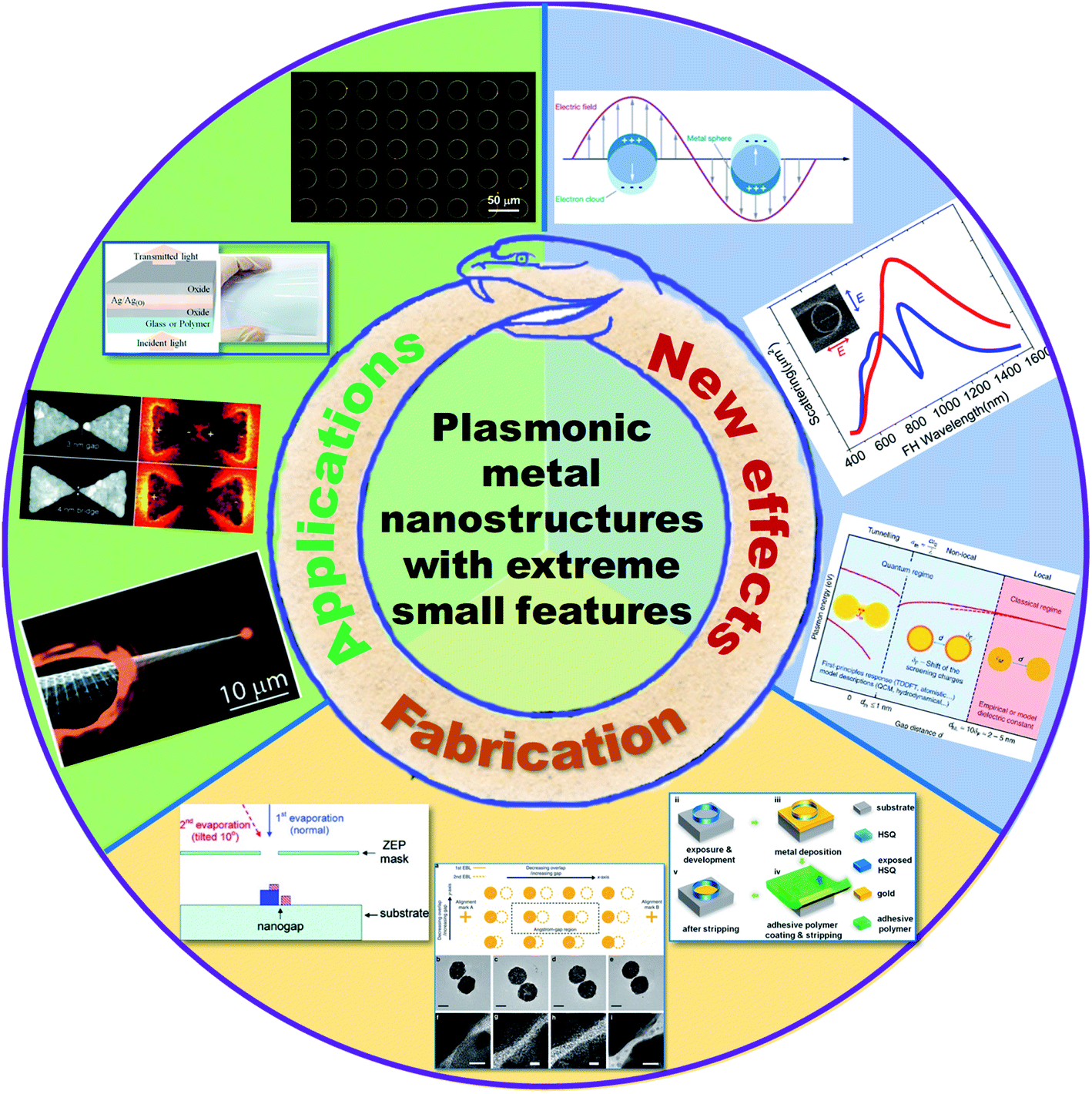
As known, the unique response of metals to incident light is dominated by the collective behavior of free electrons in metals.12 In the early 20th century, Drude first explained the collective oscillation behavior of metal free electrons by using an incident frequency dependent complex permittivity, i.e. the Drude model.13 The core idea is that the response of metals to the incident light is mainly dominated by the free electrons, mainly derived from the valence electrons, in the metal. The ions maintain the neutrality of the entire metal and do not interact with free electrons, meaning that the situation is equivalent to a large number of free electrons in a uniform metal positive ion background field. Under the first-order approximation of the Drude model, the interaction between light and metal can be regarded as the forced oscillation of a damped harmonic oscillator with a natural frequency of zero under the incident electric field E. Through the kinematics solution of the damped harmonic oscillator and the introduction of the metal macroscopic polarization, the complex permittivity and complex refractive index of the metal can be obtained respectively.The surface plasmon oscillation, the collective free electron oscillation behavior occuring at the interface between the metal and the dielectric, can propagate along the interface or be localized in the metal nanostructure, which generally includes the propagating surface plasmons (also called surface plasmon polaritons, SPP) and localized surface plasmons (LSP).14 The collectively oscillating electrons on the metal–dielectric interface form alternately distributed positive and negative charges along a certain direction of the interface, causing the collective oscillating energy of the electrons propagating forward (SPP). The oscillation frequency of SPP satisfies the dispersion relationship obtained by Maxwell's electromagnetic equations and appropriate boundary conditions, which can be expressed as,
 | (2-1) |
 | (2-2) |
SPP is a quasi-static surface bound wave; the coupling ability of incident light and free electrons and the binding ability of electric field near the interface are close to zero. As ω = 0, there is no incident light hitting the metal. As εd → −εm,  and
and 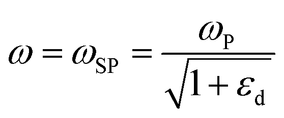 . ωSP is the limiting frequency of short wavelength, indicating that the incident light cannot be transmitted inside or on the surface of the metal and the metal exhibits extremely high reflectivity. Since the propagation constant β → ∞, the wavelength tends to zero, and the wave vector component in the normal direction of the interface tends to infinity, and the oscillating field decays rapidly in the normal direction of the interface and is greatly confined near the interface. In the small area near the interface, the effective dielectric constant of the metal–dielectric system εeff = εm + εd = 0. Therefore, the SPP is a quasi-static surface wave near the frequency ωSP. Fig. 2 shows the metal full-frequency dispersion relationship.15 In fact, the electronic damping frequency of real metal is not equal to zero (γ ≠ 0), so β does not completely approach infinity as ω = ωSP, a finite value allows a certain combination mode between ωSP and ωP.
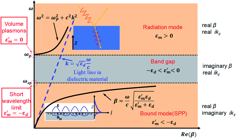 | ||
| Fig. 2 The full frequency dispersion relation of metal materials. | ||
LSP is a non-propagating surface wave formed by the coupling of free electrons in metal nanostructures and incident light. The curved surface of the metal structures can provide an effective restoring force for the collectively oscillating electrons driven by the light field. Therefore, the maximum value of field enhancement can be generated near the surface of the metal nanostructures at a specific frequency, corresponding to the localized surface plasmon resonance (LSPR).4 LSP can be directly excited by the incident light because the scattering effect of the curved surface in metal nanostructure on the incident light field makes it a wide wave vector value distribution. The optical properties of metal nanostructures are dominated by LSPR, while the resonance peak position and full width at half maximum (FWHM) of the spectra depend on the geometric parameters of the structure, material composition and the surrounding environment.
In 1908, Gustav Mie applied Maxwell's equations and appropriate boundary conditions to calculate the optical response of metal micro–nanospheres (Mie theory).16
Soon after, Richard Gans broke the limitations of Mie theory and extended it to Gans–Mie theory, being able to describe the optical response of ellipsoidal metal particles.17,18 Until then, the related theories are capable of describing most of the plasmonic metal nanostructures and corresponding effects in a reliable way.
3. Plasmonic metal nanotips (PMNTs) with ultra-small tip sizes
The investigation of the electromagnetic properties of metal tip structures can date back to the invention of the lightning rod in the early 18th-century, in which, the excellent charge conduction and localization abilities of the metal lightning rod perfectly demonstrate the most important and remarkable properties of metal tip structures. In contrast to the bulk metal lightning rod, metal nanotips demonstrate fascinating and far-reaching electromagnetic properties in optics, photonics and photoelectronics.19–24 The most remarkable plasmon effect of metal nanotips is LSPR-enabled extremely great electromagnetic field energy focus and charge localization at the tip. Such a plasmon induced high density of energy localization in an ultra-small area or a point gives rise to lots of significant applications in single molecule detection, field emission, nonlinear photonics, beyond classic light diffraction limit, high-resolution imaging energy/spectra enhancement etc.25–31It is commonly known that the geometry and dielectric environment have a great influence on the SPR behavior of metal nanostructures.32–34 In most of the PMNT involved fields, the smoother surface, smaller diameter and shaper tip are always the holy grail since the electromagnetic enhancement is inversely proportional to the feature size of the structure. Although metallic tips and tapers have been fabricated via the metallization of fibers, electrochemical etching, electron-beam induced deposition, complex multistep processes, or standard metal deposition, the controllable and efficient fabrication of high-quality PMNTs is challenging.35–38 Electrochemical etching of metal nanowires is generally the simplest strategy to obtain high quality PMNTs with an apex of around 50–60 nm, even to sub-10 nm based on the anisotropic etching rate of metal materials. As shown in the inset in Fig. 3a, the tip apex is sharper than 50 nm.39 Noble metal gold (Au) and silver (Ag) nanotips can be obtained by electrochemical etching of gold and Ag nanowires, which demonstrate high spectral enhancement ability.40 Jens Steidtner and Bruno Pettinger demonstrated an ultrahigh vacuum tip enhanced Raman technology, achieving 15 nm resolution on single dye molecule imaging with Au nanotips with radii of 15–20 nm.41 Coating noble metal Au and Ag films on electrochemically etched W nanotips is another effective electrochemical etching process to obtain high quality PMNTs. Because the charge and electromagnetic field are generally confined on the surface of the plasmonic metal structures, the W core only imposes a weak influence on the SPR behavior of the noble metal coating layer.42 In such core–shell metal nanotip structures, electromagnetic etching of the tungsten core guarantees high quality tip topology and the noble metal coating shell makes sure efficient light coupling. Besides, followed by the subsequent focused ion beam (FIB) milling process, a kind of asymmetrical Au nanotip with an end diameter of 15 nm was fabricated, showing promising application in two photon excitation near-field fluorescence imaging.43 In the fields of tip enhanced spectroscopy, detection, field emission and imaging, the tips are integrated with an atomic force microscope (AFM) and scanning tunneling microscope (STM), becoming two powerful tools in scientific studies. Benefiting from the ultra-high SPR excitation, energy focusing and about 104 field enhancement, tip-enhanced near-field spectroscopy is now able to reach ultra-high sensitivity and resolution at the single molecule/single layer molecule level.26,44
 | ||
| Fig. 3 (a) Scanning electron microscope (SEM) images of a typical Ag tip. (b and c) SEM images of a conical metallic tip with a grating coupler on the shaft and principle of the nonlocal excitation of the tip apex. (d) Micro-to nanoscale optical mode transformation on a tip. (e) Single-crystalline Au taper obtained from an electrochemical etching process. (f) Upon illumination of the grating coupler and SPPs propagate to the apex. (g and h) Schematic measurement principle and spatially resolved photoluminescence maps of Er upconversion emission. (i) SEM images of the sharp metallic pyramids (reproduced with permission from ref. 39 and 45 Copyright 2007, ref. 46 Copyright 2011, ref. 47 Copyright 2016, ref. 48 Copyright 2010, ref. 49 Copyright 2007, the American Chemical Society). | ||
The far-field coupling related nanofocusing, waveguide and nanolight source are another kind of vital fields for PMNTs. In contrast to tip-enhanced near spectroscopy, in far-field coupling systems, due to intrinsically short dephasing times and small absorption cross sections, high efficiency energy coupling, transformation and emission in metal nanotips are desperately required. Mark I. Stockman predicted theoretically that SPPs propagating toward the tip of a tapered plasmonic waveguide will slow down and asymptotically stopped when they tend to the tip, causing accumulation of energy and giant local fields at the tip.24 Such a rapid 3D adiabatic nanofocusing lays the foundation of the high-efficiency coupling of the far-field radiation to the near-field zone, where the 3D energy concentration occurs at the tip of a smoothly tapered metal nanoplasmonic waveguide.50 On the basis of this, for overcoming problems with background illumination in apertureless microscopy and higher coupling efficiency, grating coupling of surface plasmon onto metal nanotips was proposed and being used as a nano-confined light source (Fig. 3b and c).45 By writing one-dimensional gratings onto the tip of 3D tapered conical nanotips through focused gallium ion beam sputtering, Ropers et al. demonstrated an efficient nonlocal optical excitation of the apex of a nanostructured metal taper based on SPP grating–coupling.51 The SPPs propagate over more than 10 μm along the tip shaft toward the apex of the tip, where they are reradiated into the far field. Raschke et al., subsequently, found that the breakdown of the adiabatic conditions occurred only within the last 10 s of nanometers.46,52 Despite the symmetry breaking side-on illumination and the resulting SPP excitation confined along the azimuth, the tip effectively acts as a mode filter, giving rise to a propagation-induced, nanoscopic SPP excitation with radial symmetry at the apex, and suggesting the robustness of conical SPP focusing with respect to asymmetries and imperfections in the SPP generation. The resulting dipolar nanoemitter with ∼20 nm spatial confinement, that is, more than 1 order of magnitude beyond the diffraction limit, represents a novel light source. Soon after, by nanoscale field concentration via adiabatic SPP nanofocusing into monolithic Au tips, the same group demonstrated the independent nanometer spatial and femtosecond temporal optical waveform control, achieving a 10 nm spatially and few-femtosecond temporally confined excitation, as shown in Fig. 3d, showing great potential in scattering-type scanning near-field optical microscopy (s-SNOM).46 Becker and co-workers observed a coherent light scattering from a nanometer-sized metal tip-thin film gap region, finding a steep increase in scattering intensity in a near-field signal selected in k-space.47 As shown in Fig. 3e and f, this gap plasmon is different from conventional adiabatic nanofocusing determined apertureless scattering type SNOM, which allows confinement of light at the very apex of the taper to dimensions that are not limited by its apex diameter. Besides, the gap type localized plasmonic field intensity can exceed that of a bare apex mode by at least 2 orders of magnitude, revealing broader applications.
Despite the above conventional PMNTs, for specific purpose and scale-up fabricating requirements, some unconventional alien PMNTs also were purposely fabricated with various nano-fabricating techniques. Fig. 3g and h demonstrate laterally tapered planar Ag waveguide concentrated infrared surface SPPs.48 Taper/hole array microstructures are fabricated in a 140 ± 5 nm thick Ag film on the sample by electron beam lithography (EBL) followed by lift-off. By using erbium (Er) upconversion luminescence technology, the excitation, propagation, and concentration of SPPs in laterally tapered Ag waveguides are visualized. Thereafter, their study on tapered Au waveguide on a planar dielectric confirmed that SPP focusing is the dominant mechanism producing the spot of maximum intensity at the taper tip, and the nanofocusing is attributed to a guided SPP mode that has an asymmetric electric field distribution across the tapered waveguide. Park et al. fabricated vertically aligned funnel-shaped 3D PMNT arrays by directional photofluidization lithography (DPL), with which, the sharpness, shape, and orientation nanofunnel tips can be precisely controlled in a scalable and deterministic manner. A 3D plasmonic nanofocusing of light with patterned metallic pyramids is demonstrated in Fig. 3i.49 Gratings on the faces of the pyramids convert linearly polarized light into plasmons that propagate toward and converge at a ∼10 nm apex. 3D Au and Ag pyramids plasmonic light nanofocusing tip structures with smooth surfaces were fabricated by a simple and impurity-isolated template stripping process. Moreover, the plasmonic properties in a combined structure with a metallic pyramid and an integrated C-shaped aperture, metallic thin layer and a dielectric pyramidal body structure composed of a tip and one-side metal-coated pyramidal cantilever tips were also investigated, exhibiting remarkable applications in non-linear photonics.53–56
4. Plasmonic ultra-thin metal films
Ultra-thin metal films (UTMFs) are another interesting plasmonic structures with a long history. In ancient China, an ultrathin gold film was generally stuck to great Buddha to create a powerful and solemn atmosphere. After thousand times of repeated forging, a piece of thin Au plate turns into a hundred nanometer ultrathin Au film. The excellent mechanical ductility and chemical stability make sure the uniformity and corrosion resistance of the sticky Au film, enabling thousand years' shininess, holiness and resplendence of the Buddha. Currently, with the thickness of UTMFs down to the nanometer or atomic level, unique properties, such as new quantum optical effects, peculiar dielectric properties and strong plasmon field enhancement abilities lead to more exciting applications in optical sensing, imaging and flexible displays.57–59 Magnetron sputtering, thermal evaporation, electron beam evaporation, atomic layer deposition (ALD) and molecular-beam epitaxy (MBE) are traditional methods to fabricate UTMFs.57,60–62 However, large surface roughness and discontinuity of metal films are common disadvantages of sputtering and evaporation processes. Although ALD and MBE are theoretically able to control atomic level thickness and good continuity during the metal film growth, the low yield of ALD and rigorous substrate matching of MBE are bottlenecks for these two strategies.As schematically illustrated in Fig. 4, the growth of metal films is generally governed by three known models, that is, Volmer–Weber (bulk island), Frank–van der Merwe (layer by layer) and Stranski–Krastanov (layer-plus-bulk).63–65 During the growth of metal films, the presence of step and kink Ehrlich–Schwoebel effects (SESE and KESE) leads to arbitrary orientation of surface morphology. The diffusion of atoms along the steps not only affects the morphological stability of the steps, but also can induce up-step mass current leading to mound formation. Consequently, reducing the Ehrlich–Schwoebel carrier become an impactful way to improve the metal film quality.64 Introducing hybrid materials (Al, Cu, Ti Ni etc.), acting as the adsorption center and seeds to promote the nucleation of host metals, is an effective way to obtain UTMFs with small roughness.66–68
 | ||
| Fig. 4 The schematic illustration of general growth models of metal films. | ||
The inset SEM images (without (left) and with a Cu seed layer (right), the scale bars are 500 nm) and the plot in Fig. 5a demonstrate that after 1 nm of Cu seed layer deposition, atomically smooth and stable Ag films with 0.5 nm roughness on a silica substrate were successfully fabricated.69 The introduced Cu promotes nucleation, thus reducing the grain size. The same strategy was demonstrated by Al-doped Ag films, in which, 15 nm of 4% Al atom doped Ag films maintained smooth surface morphology even after 300 °C annealing in N2, exhibiting excellent thermal stability.68 The Al atoms enhance the nuclei density of films on an oxide surface due to the much larger bond strength of Al–O bonds than Ag–O bonds, and a capping layer spontaneously formed over the Al-doped Ag films restrains the surface diffusion and mass transportation of Ag atoms, strengthening the thermal stability of Ag films. The semiconductor or metal buffer layers are also crucial in fabricating sub-10 nm UTMFs.70 The surface defects of buffer layer anchor the metal atoms, decreasing the atom diffusion, and strong bonding between metal atoms and semiconductor non-metal atoms inhibits the grain growth, reducing the surface roughness. Recently, Volkov et al., depending on the monolayer MoS2 buffer layer, achieved 3–4 nm thickness ultra-thin Au films with continuous smooth morphology and Drude plasmonic response on a SiO2 substrate.71 Besides, by introducing surfactants and additives (metallic surfactants, molecular monolayer surfactants, polymer surfactants, metal additives and gas additives), seed layer-free growth, self-assembled organosilane monolayer linkers polymers etc. were also used for preparing sub-10 nm UTMFs. The substitution of metal atoms with polymers in the buffer layer decreases the cost and eliminates the subsequent deterioration of the optical and electrical properties of the metal thin films.
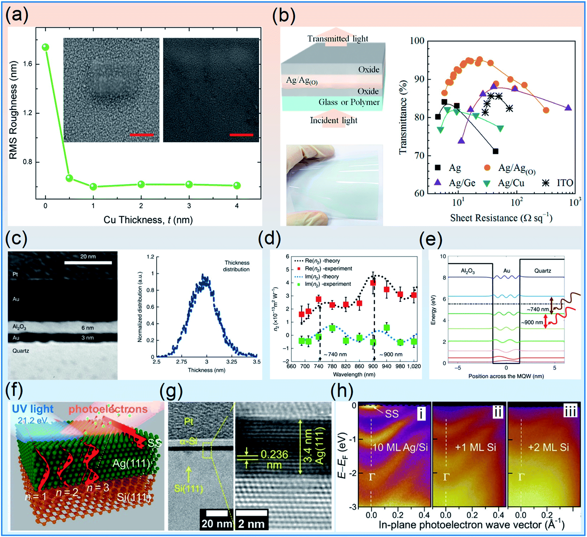 | ||
| Fig. 5 (a) Variation of RMS roughness for the 6 nm Ag film with seed layer thickness.69 (b) Comparison of total transmittance vs. sheet resistance of different flexible TEs.72 (c) Cross-sectional TEM image of the sample and the statistics of the film thickness. (d) Wavelength dependence of the Kerr coefficient and calculated quantized energy states and their corresponding wave functions (e).73 (f and g) Sketch of a Ag (111) film deposited on Si and HRTEM images of the transversal cross-section of the sample. (h) ARPES intensity as a function of electron energy relative to the Fermi energy and parallel wave vector74 (reproduced with permission from ref. 69 Copyright 2013, ref. 72 Copyright 2018, ref. 74 Copyright 2019, the American Chemical Society, and ref. 73 Copyright 2016, the Authors). | ||
For a long time, one of the most important applications of UTMFs is the transparent electrodes in flexible devices.75 The strong SPR, high electrical conductivity and low loss in visible and near-infrared of Ag and Au make them perfect substitutions for traditional indium tin oxide film (ITO) film materials. The good malleability and flexibility of Au and Ag UTFMs bridge the gap between rigid ITO films and flexible photoelectrical devices. More importantly, the general UTMF fabrication methods are compatible with standard CMOS (complementary metal-oxide-semiconductor transistor) and MEMS (micro-electromechanical systems) nano-manufacturing, promising better compatibility and integrated performance.76 Yun's group demonstrated a nitrogen-doped copper film with an average transmittance of 84% over a spectral range of 380–1000 nm and a sheet resistance lower than 20 Ω sq−1. The corresponding flexible organic solar cell achieves a power conversion efficiency of 7.1%, exceeding that (6.6%) of solar cells utilizing the conventional ITO film (Fig. 5b).72 In the flexible photoelectrical device field, Liu et al. demonstrated giant Kerr response of ultrathin Au films from quantum size effects in metal quantum well (MQW) structures (Fig. 5c–e).73 The measured nonlinear Kerr susceptibility reaches 2.06 × 10⁻¹⁵ m−2 V−2, showing a four orders of magnitude enhancement compared with the intrinsic value of bulk Au. Compared with the LSPR based nonlinear effects, the MQWs have the advantages of broadband operation and free of scattering, promising high compatibility with existing nano-photonic waveguides for integrated nonlinear optics. Moreover, although the SPR on metal films is generally localized on the surface of the film, new SPR effects occur as the thickness scales down to several atoms of UTMFs. Compared to the 5 nm thick Au film, the 3 nm thick Au film fabricated by a cryogenic temperature deposition process not only displays improved transmittance, but also degraded relative electric permittivity, revealing decreased plasmonic adsorption. El-Fattah et al. demonstrated wafer scale 8 atomic monolayer (∼1.9 nm) crystalline Ag films with excellent plasmonic and electrical properties, as shown in Fig. 5f–h.74 Despite the plasmonic resonance shift, they also obtained sharp near-infrared optical spectra with a quality factor of ∼4 and strong plasmon localization in such an atomic UTMF, suggesting great potential for electro-optical modulation and optical sensing applications. Recently, Pruneri and co-workers demonstrated plasmons in few-nanometer-thick Au UTMFs, with clear evidence of new dispersion regimes and large electrical tunability.77,78 Resonance peaks at wavelengths of 1.5–5 μm are shifted by hundreds of nanometres and amplitude-modulated by tens of percent through gating using relatively low voltages. Combined with a large-scale fabrication approach, the fabricated films can find applications in transparent conductors, plasmon-enhanced spectroscopy, optical biosensing and electrochromic devices.
Beyond the new plasmonic effects and applications mentioned above, UTMFs imply broader future applications in the fields of optoelectronics, nonlinear optics, plasmon-enhanced detection and sensing, thermal manipulation, two photon emission and plasmonic color printing.79–81
5. Quantum plasmonics in ultra-small metal particles
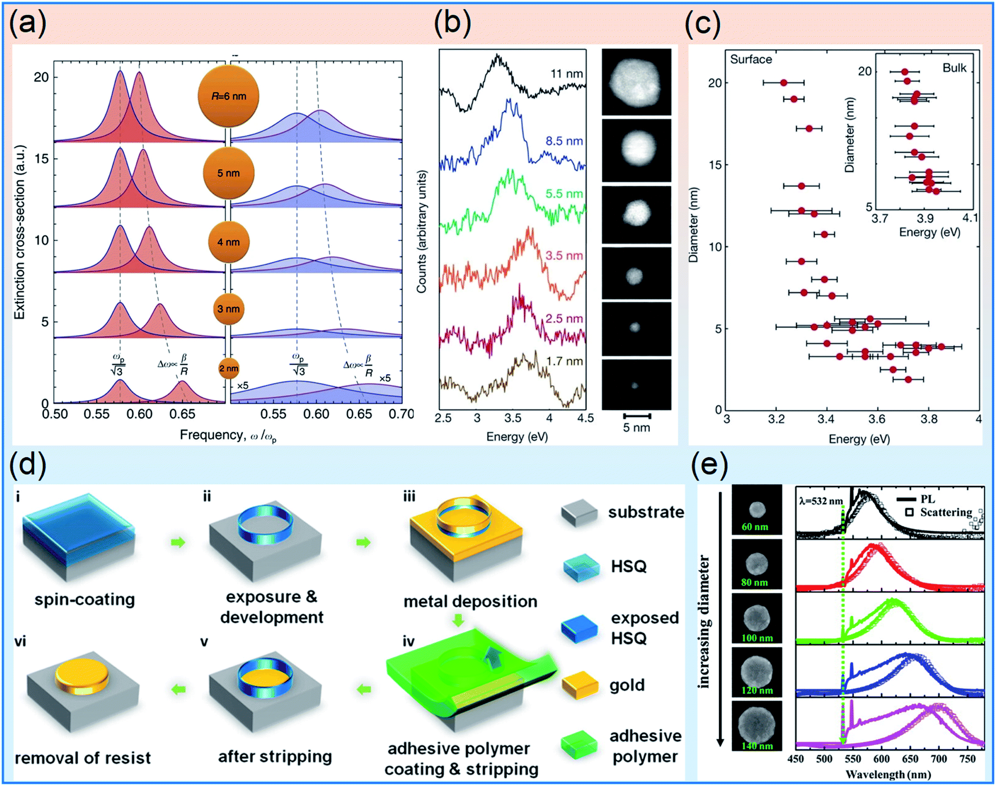
Ultra-small metal particles (USMPs) are one of the simplest but extraordinarily vital plasmonic structures. With the decease of particle size, the plasmonic behaviors of USMPs evolve from classical electrodynamic theory to quantum theory. The quantum size effect, nonlocal effect, electron density spill-out and tunneling effect become prominent as the particle size scales down to the sub-nanometer scale.82–88The plasmonic spectrum of a single noble metal spherical nanoparticle experiences a blue-shift with the gradual decrease of the particle size, and such a dependence can be well-described by classical electrodynamic theory. However for USMPs with size smaller than ∼2 nm, things seem to go in a confused way, both blue-shift and red-shift of plasmonic spectra appeared.89,90 The underlying reason is that as the particle size scales down to the sub-nanometer scale, the quantum effects cannot be neglected. In certain circumstances, the quantum effects even play a dominating role in determining the spectral behaviors of the USMPs. In 1987, S. Das Sarma investigated the surface-plasmon excitation in simple metals using a hydrodynamical model based on an electron gas-based nonlocal theory.82 The infrared divergence inherent in local theories is suppressed by nonlocal corrections, and as the velocity of the probe particle vanishes, the excitation probability goes to zero. He also showed that for low energy external protons interacting with the metal surface, nonlocal effects reduce the excitation probability compared with the local theory. For a long period, such nonlocal theories prevail in many quantum plasmonic systems. In 2014, Mortensen et al. put forward a comparatively simple semiclassical generalized non-local optical response theory that unifies quantum pressure convection effects and induced charge diffusion kinetics for plasmonic nanostructures.91 The theory described both the frequency shifts and size-dependent damping in individual metallic nanoparticles as well as the broadening of the crossover regime from bonding dipole plasmons to charge-transfer plasmons in plasmonic nanoparticle dimers (Fig. 6a). However, with hard-wall boundaries, the standard hydrodynamic Drude model is capable of giving out accurate quantitative predictions for the optical response of plasmonic metal nanoparticles. For the nanosystem where the surface effect caused by the electron density spill-out in free space cannot be neglected, the standard hydrodynamic Drude model is less accurate. Toscano et al. studied the resonance shifts and spill-out effects in self-consistent hydrodynamic nanoplasmonics.92 They constructed a self-consistent hydrodynamic model to explain the size-dependent surface resonance shifts of Na and Ag nanowires and nanospheres. The theory provides a good attempt to develop a versatile hydrodynamic theory and numerical method that account for both retardation and electronic spill-out.
 | ||
| Fig. 6 (a) Extinction cross-section for the dipole resonance in a metal sphere.91 (b) Collection of normalized, deconvoluted EELS data from Ag particles. (c) Plot of the SPR energy versus particle diameter, with the inset depicting bulk resonance energies.93 (d) Schematic illustration of the “SPL” approach.94 (e) PL of Au nanodisks with different sizes95 (reproduced with permission from ref. 91 Copyright 2014, ref. 93 Copyright 2012 Springer Nature, ref. 94 Copyright 2016 and ref. 95 Copyright 2012, the American Chemical Society). | ||
Yet with lots of challenges, the experimental investigation on USMPs also demonstrates exciting advances. The theoretical descriptions and experimental results of USMPs with size larger than 10 nm are well matched under the classical electrodynamic framework, and will not be the main points here. The USMPs or clusters are generally synthesized by bottom-up wet chemical processes, and in some occasions, ligands are indispensable in precise control of the cluster size and atom numbers. The addition of ligands may weaken the optical response of metal USMPs and clusters due to metal–ligand interaction. In 2012, Scholl et al. synthesized individual ligand-free silver nanoparticles and investigated the plasmon resonances by aberration-corrected TEM imaging and monochromated scanning TEM electron energy-loss spectroscopy (EELS).93 They found that as the diameter of nanoparticle decreases from 20 nm to less than 2 nm, the plasmon resonance blue-shifts to higher energy by 0.5 eV, which is a substantial deviation from classical predictions, indicating a transition to the quantum-influenced regime (Fig. 6b and c). Soon after, Haberland pointed out that the blueshift of LSPR with the decrease of particle size in Scholl's work is flawed, because they neglected the influence of the carbon substrate and possibly the residual ligand. A convincing way is taking both the small and large size limit into account in the study of size dependent plasmon resonance in metal nanoparticles.90 Therefore, what is the small-particle limit of the surface plasmon becomes an unavoidable and fundamental question to be answered.
In 2016, Zhou et al. carefully studied the evolution from the plasmon to exciton state in ligand-protected atomically precise gold nanoparticles.96 They investigated the transition from the metallic (or plasmonic) to molecular state in metal nanoparticles by performing ultrafast spectroscopic studies based on atomically precise thiolate-protected Au25, Au38, Au144, Au333, Au∼520 and Au∼940 nanoparticles. Three distinct states: metallic (size larger than Au333, larger than 2.3 nm), transition regime (between Au333 and Au144, 2.3–1.7 nm) and non-metallic or excitonic state (smaller than Au144, smaller than 1.7 nm) are clearly demonstrated. The results of CO oxidation and electrocatalytic oxidation of alcohol proved that the transition state apparently impacts the catalytic ability of the nanoparticles, providing a solid guide to the synthesis of atomic metal catalysts in the catalysis process. Furthermore, Higaki and co-workers observed sharp transition from nonmetallic Au246 to metallic Au279 with nascent SPR using thiolate-protected Au nanoparticles.89 By femtosecond transient absorption spectroscopic analysis and steady-state absorption spectroscopy, they found that the Au279 nanocluster shows the metallic state of the particle while Au246 displays a nonmetallic electronic structure of the nanocluster. The findings are surprising that only 33 gold atoms lesser of Au246 than that of Au279, but the optical properties and electron dynamics between Au246 and Au279 are dramatically distinguished from each other. Recently, Wang's group investigated the plasmonic evolution of atomically size-selected Au clusters by electron energy loss spectroscopy (EELS).97 They systematically investigated the plasmonic response of Au clusters with atom number (N) from 100 to 70![[thin space (1/6-em)]](https://www.rsc.org/images/entities/char_2009.gif) 000. The bulk plasmon remains unchanged above Au887 and disappears as N decreases to 887. The SPR firstly redshifts from 2.4 to 2.3 eV above Au887 and blueshifts towards 2.6 eV down to Au300 and finally splits into 3 fine features. Naturally, an evolution picture of plasmon physics with atomically-precise was revealed and divided to 3 regimes, i.e. classical plasmon (Au887 to Au70000), quantum confinement corrected plasmon (Au300 to Au887) and molecule related plasmon (particle size less than Au300). The observations from solid-state plasmon classical electrodynamics, quantum confinement corrected plasmon physics, and molecular plasmon theory pave the way for novel applications of plasmonic USMPs. Note that the changes in crystal structures during the size decrement are also the vital phenomena that should be considered in investigating the quantum size effects of USMPs.98,99
000. The bulk plasmon remains unchanged above Au887 and disappears as N decreases to 887. The SPR firstly redshifts from 2.4 to 2.3 eV above Au887 and blueshifts towards 2.6 eV down to Au300 and finally splits into 3 fine features. Naturally, an evolution picture of plasmon physics with atomically-precise was revealed and divided to 3 regimes, i.e. classical plasmon (Au887 to Au70000), quantum confinement corrected plasmon (Au300 to Au887) and molecule related plasmon (particle size less than Au300). The observations from solid-state plasmon classical electrodynamics, quantum confinement corrected plasmon physics, and molecular plasmon theory pave the way for novel applications of plasmonic USMPs. Note that the changes in crystal structures during the size decrement are also the vital phenomena that should be considered in investigating the quantum size effects of USMPs.98,99
Compared with ultra-small clusters synthesized by bottom-up wet chemistry, the artificial metal atoms/molecules fabricated by top-down techniques, such as EBL, FIB, chemical etching RIE etc., possess much larger size. However, benefiting from the better size and morphology control ability of top-down nanofabrication approaches, the investigation on the plasmonic optical properties and applications of artificial monomer atoms is always of great importance and desirable.100
To overcome the low efficiency and high time-consumption of transitional top-down approaches, recently, our group developed a “Sketch and Peel” lithography (SPL) approach for large scale, high efficiency, multiscale and high precision metal nanostructure fabrication (Fig. 6d).94 By taking the method analogous to paper-cutting, in the SPL approach, only the outside outlines of nanostructures are needed to be exposed, which greatly improves the fabrication efficiency of EBL. Moreover, the effective inhibition of the proximity effect enables ultra-high precision and shape control ability. We estimate that the fabrication efficiency is improved by hundreds of times. By extending the idea to the FIB process, we found that the SPL process is compatible to state-of-the-art helium ion beam milling technology and both the fabrication efficiency and precision are greatly improved.101 Furthermore, by introducing a self-assembled monolayer to engineer the surface energy of the substrate, the adhesiveness of the Al film outside the outline template is significantly decreased to implement the selective peeling process, and various plasmonics Al nanostructures with sub-20 nm feature sizes were successfully achieved by the SPL approach, suggesting the tremendous potential and fabricating ability of the technology.102–104 With regard to optical properties and applications of artificial plasmonic metal atoms, the hybridization model for the plasmon response of complex nanostructures provides a simple effective guideline.105 As shown in Fig. 6e, Hu et al. performed a systematic study on the photoluminescence (PL) and scattering spectra of EBL defined individual Au nanodisk structures.95 They found that the PL spectra and scattering spectra of individual Au nanodisks showed the same dependencies on shape, size, and plasmon coupling as the particle plasmon resonances, providing conclusive evidence that the PL in Au nanostructures indeed occurs via radiative damping of plasmon resonances driven by excited electrons in the metal itself and the PL peak position can be adjusted by their plasmon resonances. Subsequently, Chen et al. found that the Cr adhesion layer between the SiO2 substrate and Au nanostructures not only weakens the scattering intensity of the structures, but also leads to the red-shift of the spectral position.106 Lawrence J. Tauzin et al. explored the relationship between plasmon damping and PL in Au nanorods. The damping resulting from poor crystallinity in nanostructures and adhesion layers can be quantitatively linked to the decrease in PL quantum yield, and the annealing process can improve the emission intensity of lithographically prepared Au nanorods.107
6. Plasmon coupling in metal nanogaps
Plasmon metal nanogaps, have a unique and vital position in light–matter interactions. Sub-nanometer metal nanogaps are able to focus the incident light into the region beyond the classic diffraction limit, and have wide applications in subwavelength waveguides, molecular detection, plasmonic antennas, medical treatment, and nano-optics.108–112 As the distance of nanogaps scales down to sub-nanometer, some quantum effects, such as nonlocal electromagnetic effects, optical rectification, inelastic electron tunneling, rings interference generally emerged (Fig. 7).113 In this small section, we will briefly give a comprehensive discussion on the typical advances in theories, fabrication and applications of sub-nanometer nanogaps. | ||
| Fig. 7 The impact of quantum mechanical effects on plasmonic resonances113 (reproduced with permission from Copyright 2016, the Authors). | ||
Plasmonic metal split rings (PMSRs) with sub-nanometer split gaps
The PMSR nanostructure with a sub-nanometer split gap is a crucial and unique gap structure, in which, generally, the distance of split gaps can be well-controlled by top-down fabrication processes. For large metal split rings, the main attention is focused on their excellent applications in THz applications.110 For PMSRs with sub-nanometer split gaps, top-down EBL and FIB are two of the most vital and popular techniques. Besides, new strategies and methods are also demonstrated. For example Gwinner et al. proposed a fast and cheap, large-area, high-coverage shadow nanosphere lithography technique to fabricate periodic metallic split-ring resonator structures.114 In this fabrication process, the inner- and outer-ring diameters, gap angles, as well as thickness and periodicity of the metallic split-ring resonator structures can be well controlled.The unique geometry structures of PMSRs with sub-nanometer split gaps enable them with many attractive nonlinear effects, such as pronounced Fano resonance, high-order harmonic wave generation and light twisting. For example, Cao et al. designed gradient–rotation split-ring antenna metasurfaces to simultaneously generate and separate pure optical vortices in a broad wavelength range, which has the potential in miniaturized on-chip orbital angular momentum-multiplexers.115 As shown in Fig. 8a and b, by hybridizing with nanodisks, the split-ring resonators/disk nanocavities with strong Fano resonance are capable of generating high-order magnetic modes, indicating great promise in refraction index sensors.116 Besides, multiple-split rings with sub-nanometer feature sizes can confine the LSPR and the associated field enhancements to specific areas, meaning higher flexibility in manipulating the parameters of field hot spots, thus leading to higher capability and availability for sensing.117 More interestingly, by decreasing the inner radius of split rings to zero, split nanodisks are obtained. Fang et al., introduced a single metallic nanodisk with a missing wedge shaped slice to support a Fano resonance, in which, the coupling between a hybridized plasmon resonance of the disk and a narrower quadrupolar mode supported by the edge of the missing wedge slice supports the Fano line.118 Very recently, we demonstrated the pronounced Fano resonance in the near-infrared region using Au split nanodisk structures fabricated by the SPL process. The ultra-small split gaps of 15 nm enable strong plasmon coupling and field enhancement in the gap region.119 The Fano resonance behavior can be easily controlled by changing the disk diameter and split length. We found that the Fano resonances observed in the split nanodisks are induced by mode interference between the bright antibonding dipole mode of split disks and the subradiant mode supported by the narrow split gap. Enabled by the giant near-field enhancement, strong wavelength-dependent second harmonic generation was observed under near-infrared excitation in split nanodisks (Fig. 8c and d). Recently, a tunable dual-split-disk resonator composed of top and bottom Au split-disk resonators in the THz wave was theoretically demonstrated, which exhibits electromagnetically induced transparency characteristics and a high merit factor, showing potential in sensing, programing, filtering, and attenuating devices.
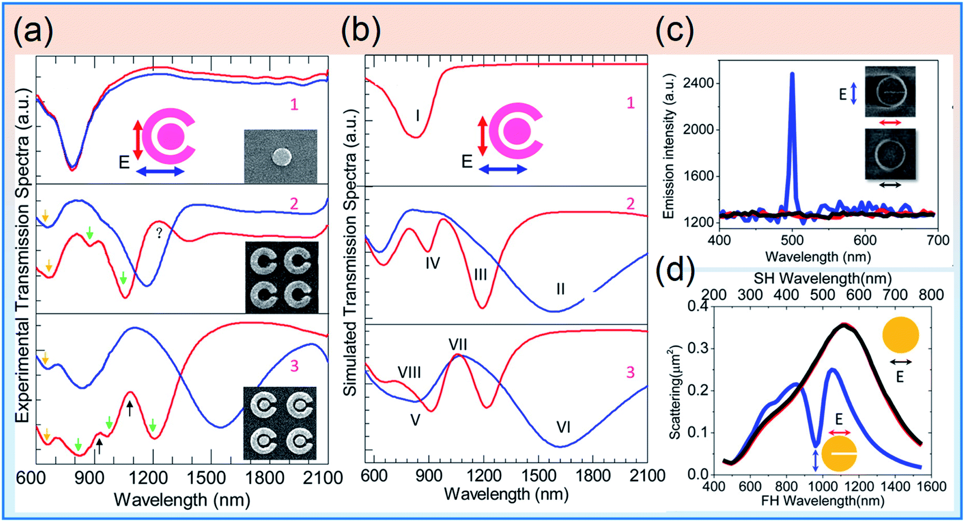 | ||
| Fig. 8 (a and b) Experimental (a) and calculated (b) transmission spectra of disk (1), SRR (2), and SRR/D (3) arrays.116 (c and d) Measured SH emission and SH emission intensity versus the incident wavelength (c) and calculated scattering spectra (d) for the single split and perfect nanodisks119 (reproduced with permission from ref. 116 Copyright 2013 and ref. 119 Copyright 2016, the American Chemical Society). | ||
Artificial plasmonic metal nanoparticle pairs (APMNPs) with sub-nanometer nanogaps
Two closely positioned APMNPs with sub-nanometer nanogaps are the simplest and extremely significant nanostructures in the plasmonic coupling field. The high controllability in fabricating artificial plasmonic molecules by top-down micro/nano-manufacturing methods makes APMNPs an ideal candidate to explore new effects in sub-nanometer gap size structures. Generally, the gap regions, the so-called electromagnetic energy “hot spots”, enable huge field density and large intensity enhancement, thus leading to great potential in sensing and detection.120 The gap distance between two nanoparticles can be precisely controlled. With the gap size of APMNPs down to sub-nanometer, the associated optical properties also experienced a transition from classic electrodynamics to quantum dynamics, that is, the quantum nonlinear effects, such as size effect, nonlocal effect, electron spill-out effect, Coulomb block effect and quantum tunneling effect will gradually become pronounced.121In general, top-down and bottom-up nanofabrication techniques are all capable of fabricating paired metal nanoparticles with sub-nanometer gaps.122 Compared to highly controlled top-down approaches, bottom-up wet chemical synthesis processes are more superior in obtaining ultra-small nanogaps.123 However, both techniques have shortcomings in fabricating APMNPs with sub-nanometer gaps, so optimizations on high-efficiency, reliability and time/economy consuming fabrication approaches are always desirable and indispensable. In top-down methods, the proximity effect in lithography is the biggest challenge. In 2002, Liu et al. developed an automated proximity effect correction algorithm based on the self-consistent exposure equalization technique to fabricate electrode pairs.124 Koh et al. patterned triangle dimers with sub-1 nm gaps on electron-transparent 30 nm thick silicon nitride transmission electron microscope (TEM) windows based on the fact that the substrate with lower density and atomic number could greatly reduce the range and intensity of the proximity effect during the lithography process.125 In 2010, Theiss et al. demonstrated an angle evaporation technique that can fabricate arrays of plasmonic nanoparticles with the gap size of 1 nm (Fig. 9a).126 As shown in Fig. 9b, a two-step EBL process to decrease overlap was proposed by Zhu and Crozier, and metallic dimers with angstrom-scale gaps were achieved.127 Lately, Hoogenboom's group developed an electron-beam induced deposition etch mask method, achieving Au dimers with sub-10 nm spacing distance.128 For the FIB process, Ga-ion beams generally only can obtain structures with gap size larger than 10 nm due to the low resolution. Carl Zeiss Company reported a 4 nm nanogap on a suspended Au film obtained using He-ion lithography.129 Recently, by combing EBL, reaction ion etching, HF etching and Ga+ FIB milling processes, Cui et al. developed a method to produce ∼2 nm Au gap electrodes.130 Our group also developed a series of EBL-based approaches to reliably fabricate nanostructures with sub-10 nm gaps (Fig. 9c).94,101–104,119,131–139 Besides, other methods such as capillary-force self-assembling of patterned nanostructures, tip-based approaches, controlled metal deposition and breaking or crack strategies are also able to achieve sub-10 nm gap APMNPs, which recently have been reviewed by Yang et al., and will not be discussed in this paper.140
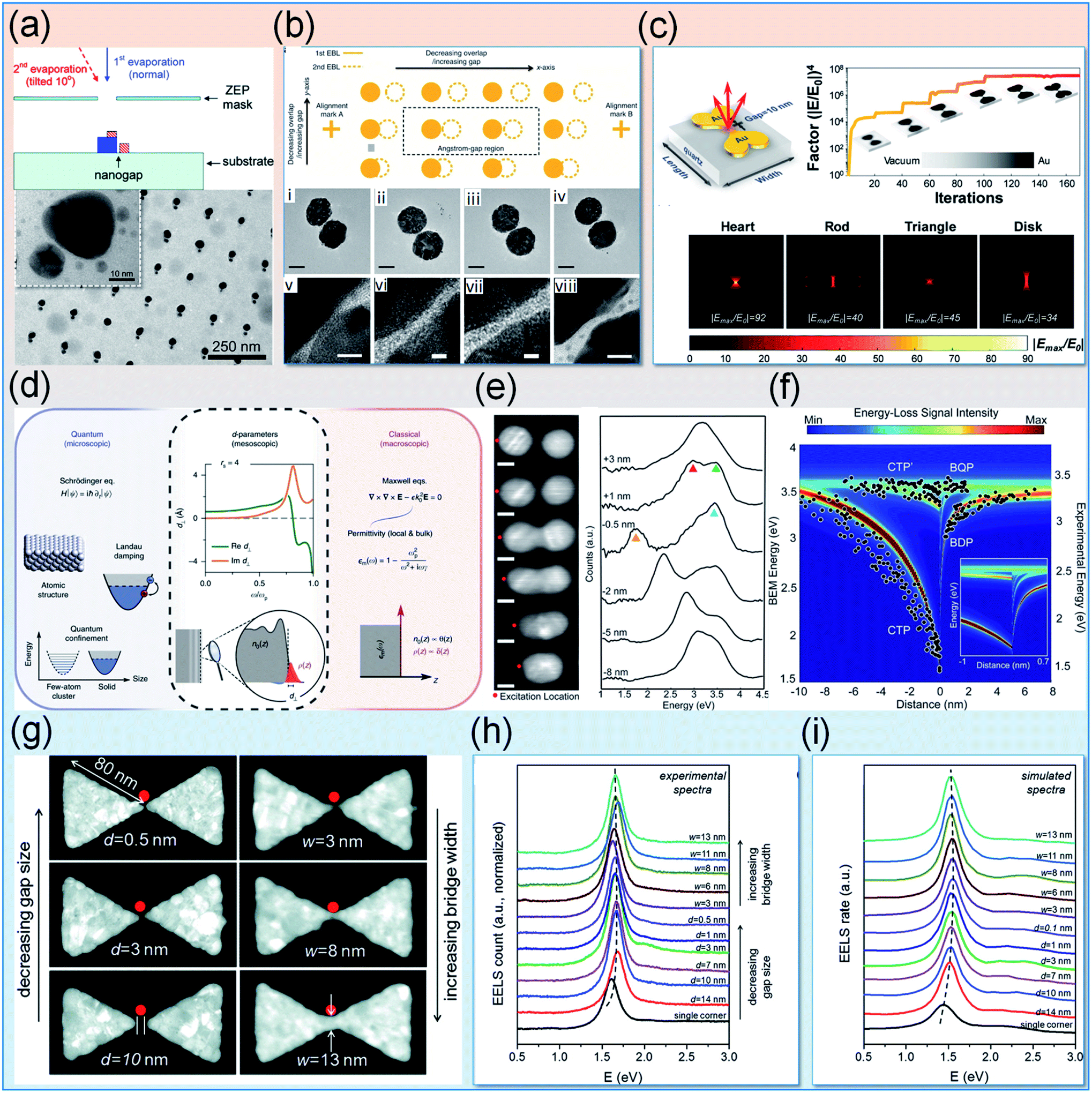 | ||
| Fig. 9 (a) Schematic diagram of the angle evaporation technique and the SEM of obtained nanostructures.126 (b) Schematic depiction of the two-step EBL process and TEM images of four representative dimers.127 (c) The 3D model and the electric-field distribution of heart-, rod-, triangle-, and disk-shaped Au nanoparticle dimers.102 (d) Nonclassical mesoscopic electrodynamics via d-parameters.141 (e) STEM images correlated with experimental plasmonic spectra and theoretical field profiles of a merging dimer. (f) Comparison of classical BEM EELS calculations with experimental EELS resonances.123 (g–i) Representative HAADF STEM images of the experimental samples with different junction geometries (g), experimental EELS spectra (h) and simulated spectra (i) of the dark modes of structures136 (reproduced with permission from ref. 102 Copyright 2020 Wiley-VCH, ref. 123 Copyright 2013, ref. 126 Copyright 2010 and ref. 136 Copyright 2012 the American Chemical Society, ref. 127 Copyright 2014, Nature Publishing Group, ref. 141 Copyright 2020, the Authors). | ||
To better understand and illustrate the optical response transition of APMNPs from classic to quantum effects, innovative advances and developments are presented uninterruptedly in the past few decades. Early studies on the quantum tunneling exposed that when the “hot spot” between two Ag nanospheres is small, its local field is almost identical to a replaced plate.142 As the gap size is smaller than 0.6 nm, the quantum tunneling will dramatically reduce the enhancing ability of the interstice between nanoparticles.143 In 2011, Esteban et al. proposed a quantum-corrected model that incorporates quantum-mechanical effects within a classical electrodynamic framework.144 Tserkezis et al. carefully studied the underlying reasons for nonlocal damping induced plasmon-enhanced fluorescence reduction in ultra-narrow gaps.145 Recently, by incorporating Feibelman d-parameters, as displayed in Fig. 9d, Gonçalves and co-workers demonstrated that the neglect of quantum effects in sub-nanometer gap structures can be well-remedied in a unified theoretical treatment of mesoscopic electrodynamics, which bridged the gap between the purely quantum and classical domains.141 Along with theoretical advancements, experimental investigations on the quantum effects of APMNPs also showed enormous progress. Baumberg's group revealed the quantum regime of tunneling plasmonics by measuring the electrical and optical properties of Au nanostructures with controllable sub-nanometer separation at the same time.122 Combining with the quantum models of plasmonic systems, the singularities predicted by the classical theories were eliminated. Their experimental results suggest that the quantum tunneling constructs a quantum limit for plasmonic field confinement (∼10−8λ3 for visible light). In 2013, by employing STEM and EELS, Scholl et al. demonstrated the observation of quantum tunneling between two coupled plasmonic Ag nanoparticles as the gap size is reduced to atomic dimensions.123 Their observations demonstrate a gradual transition from classical calculations to quantum theories, accompanied by the transition of optical spectra from the redshift of the dominant dipolar peak to electron tunneling induced intensity reduction as the gap size is gradually reduced from 7 nm to smaller than ∼0.5 nm (Fig. 9e and f). Furthermore, the bonding dipolar mode is substituted by a dipolar charge transfer mode in the overlapped particle systems. Nijhuis et al. presented another interesting quantum plasmonic gap system, a molecular tunnel junction, composed of self-assembled monolayer bridged plasmonic resonators at length scales in the range of 0.4 to 1.3 nm. The tunnel barrier width and height can be controlled by the properties of the molecules. Depending on EELS, they directly observed the showing that the potential plasmonic induced tunneling can be observed in reconciling molecular electronics.146
It is worth noting that artificial plasmonic metal dimers are also crucial parts in revealing the quantum size effects of APMNPs with sub-nanometer gaps. Artificial metal dimer molecules are the simplest inter-coupling structures that are composed of two “atoms”. The inter-coupling of two “atoms” makes metal dimers having more complex LSPR modes.122,147–151 Zuloaga et al. proposed a fully quantum mechanical description of the plasmon resonances in a metal dimer by using time-dependent density functional theory, showing that for gap sizes below 1 nm quantum mechanical effects will greatly shape the optical response and drastically decrease the field enhancements relative to classical predictions.152 In 2012, we fabricated nanoprisms with varying gap and bridge widths. By systematic reduction of the gap to 0.5 nm size and narrowing the bridge to 3 nm width (Fig. 9g), we observed, for the first time, the gradual appearance of the charge-transfer plasmon mode and identify higher-order antenna modes, shedding light on the evolution of plasmon modes in the transition regime from a disappearing gap to a conductive bridge between two metal nanoprisms (Fig. 9h and i).136 One year later, we developed a three-dimensional nonlocal hydrodynamic solution of Maxwell's equations and investigated the electron-energy loss probing of nonlocal effects in metal structures below the nanoscale.132 For connected bowties, we showed that it is the dipole–dipole mode that is most affected by nonlocality, resulting in blueshifts as large as 0.7 eV for a dimer made up of prisms with a side length of 5 nm. The experimental EELS for Au nanoprisms connected by bridges as narrow as 1.6 nm indicated that nonlocal effects do not appear to be pronounced. In such nanoprisms, quantum confinement and granularity at the nanometer scale need to be taken into consideration. In addition to classic boundary limit investigation, nonlinear effects and corresponding application of plasmonic metal dimers are also inspiring. Capasso et al. reported a bowtie plasmonic quantum cascade laser antenna that can confine coherent mid-infrared radiation well below the diffraction limit, showing great potential in spatial-resolved high-resolution chemical and biological imaging and spectroscopy.153 Soon after, nanogap detectors for fast DNA analysis,154 high-harmonic generation devices,147,155 and single-molecule sensing systems based on artificial plasmonic metal dimers with sub-nanometer gaps are also demonstrated.156–158 Moreover, the single-particle level sensor composed of two different materials can be achieved by a named hetero-plasmonic dimer.159 Wang's group systematically investigated the coupling behaviors of 2D homo- and hetero-plasmonic dimers with universal sub-10 nm gaps. They found that compared with homo-dimers of Au–Au and Ag–Ag, the primitive Au and Ag plasmon modes differ in energy, leading to much weaker hybridization.160
3D plasmonic metal nanostructures (3D-PMNs) with sub-nanometer gaps
3D-PMNs are more effective than those supported by in-plane coupling since the coupling between plasmonic structures and the supported substrates weakens the inter-coupling of plasmonic metal structures. With added dimensions, decoupled 3D-PMNs enable higher flexibility in geometric structures, coupling modes and possible applications. 3D-PMNs are capable of many amazing properties and applications, including geometric and coupling mode variabilities, decreased substrate-induced loss and enhanced plasmon coupling efficiency. Besides, high-aspect ratio nanostructures are potentially of great importance in biological sensing and X-ray diffraction.Hatab et al. described plasmonic interactions in suspended Au bowtie nanoantenna with sub-10 nm gap distance by EBL and following metal deposition processes, achieving up to 2 orders of magnitude additional enhancement compared with that of bowtie structures directly attached on substrates (Fig. 10a).161 The improved SERS enhancement is attributed to a plasmonic nanocavity effect occurring when the plasmonic interactions enter a strongly coupled regime. Wang's group's described a 3D plasmonic Au mushroom array refractive index sensing with a Wood's anomaly and the LSPR interference induced figure of merits of ∼108, which is comparable to the theoretically predicted upper limit for standard SPP resonance sensors.166 In 2014, Chirumamilla and co-workers introduced novel complex 3D star-shaped Au nanostructures with interparticle spacing below 10 nm by EBL and the subsequent reaction-ion etching approach. Endowed with multiple tips that are decoupled from the substrate, the 3D Au nanostar dimer exhibits the ability for single-/few-molecule detection by SERS.167 Soon after, the same group fabricated bimetallic 3D nanostar dimers in ring cavities, achieving the recyclable and robust SERS substrates for signal detection from few molecules (Fig. 10b and c).162 Very recently, Wu et al. fabricated high aspect-ration collapsible nanofinger-like plasmonic structures with precisely controllable nanogaps of sub-10 nm by combining nanoprinting lithography, reaction-ion etching, metal deposition and ALD processes. Depending on this approach, they simultaneously observed fluorescence and the Raman signal in the same spectra, providing an opportunity to analyze plasmon enhanced fluorescence with in situ local field enhancement monitoring.168
 | ||
| Fig. 10 (a) Schematic illustration of elevated Au bowties on top of Si posts, the calculated spatial distribution of the E field intensity, SEM image and SERS spectra of bowtie substrates.161 (b and c) The fabrication process (b) and SEM image (c) of AgAu 3D nanostar dimer.162 (d) The schematic illustration of atomic layer lithography. (e) The top-view SEM of a 5 nm-wide annular gap in a 200 nm–thick Ag film.163 (f) Schematic flow and corresponding SEM images in each stage of the fabrication process used for the coaxial nanocavity array using glancing-angle ion polishing.164 (g) Conceptual schematics of the self-folding of nanocylinders with plasmonic nanogaps for bimolecular sensing165 (reproduced with permission from ref. 161 Copyright 2010, ref. 162 Copyright 2014, ref. 164 Copyright 2016, ref. 165 Copyright 2020, the American Chemical Society, and ref. 163 Copyright 2013, Nature Publishing Group). | ||
Another interesting 3D PMNs are vertically oriented gap structures with the gap size less than 1 nm, which are mainly demonstrated by Kim and Oh et al. in the University of Minnesota.163,164,169–175 In 2013, as shown in Fig. 10d and e, they introduced an atomic layer lithography process and successfully fabricated wafer-scale vertically oriented gaps in opaque metal films along the entire contour of a millimetre-sized pattern, with gap widths as narrow as 9.9 Å.163 With such reliable ultra-small nanogaps, they not only observed resonant transmission of near-infrared waves through 1.1 nm-wide gaps (l/1295, an effective refractive index of 17.8), but also a resonant transmission of millimetre waves through 1.1 nm-wide gaps (l/4000000, inferring a field enhancement factor of 25000). The method is capable of producing sub-nanometer gaps over millimetre-scale contours, enabling resonantly enhanced transmission of THz waves. Soon after, based on the same approach, they experimentally demonstrate that even the refractive index change produced by only a 1 nm thick dielectric overlayer (Al2O3 film) can be detected by the THz waves confined in sub-10 nm metallic gaps.170 Besides, the method is also extended to the high-throughput fabrication of resonant metamaterials with ultra-small coaxial apertures by combining with glancing angle ion polishing (Fig. 10f). The constructed ultra-compact, high aspect-ratio coaxial nanocavities with 2 nm gaps and 100 nm diameters exhibit higher order resonances at optical and the zeroth-order F–P mode frequencies.164 Recently, they further demonstrated the broader applications of these vertically oriented gap structures with sub-10 nm gaps in low-power optical trapping of nanoparticles and proteins, high-contrast infrared absorption spectroscopy, and nanogap electrodes, as well as mid-infrared nonlocality and quantum plasmonics.169,171,175–178 The work on vertically oriented gap structures with sub-1 nm structures greatly strengthens the power and ability of extreme small gap structures, which also promise more possibility and potential in metal plasmonic nonlinear optics and plasmonic quantum photonics.
Beyond top-down micro/nanofabricating processes, Dai et al. demonstrated a self-assembled 3D nano-split ring originating from a 2D nanobelt for plasmon-enhanced optofluidic sensing (Fig. 10g). The realized segmented nanocylinders were achieved by electron irradiation triggered self-assembly. The optical response of the 3D plasmonic nanostructures shows an intensity enhancement over 22 times.165 Although, 3D PMNs generally enable higher coupling efficiency, the difficulties in precisely and large scale fabricating of 3D-PMNs inhibit the practical applications, the advances and breakthroughs in the more efficient and economic approaches will have heavy impact on the fields.
7. Summary and outlook
In summary, plasmonic metal nanostructures with extremely small feature sizes play crucial roles in the fields of nanophotonics, sensing, nonlinear optical effects, spectral filtering, high-resolution imaging, light focusing and quantum optics, especially in the areas that are beyond the ability of conventional devices, such as quantum nonlocality, quantum tunneling and high-order harmonic wave generation. Nowadays, motivated by the pursuit of scientific limit and technological innovation, plasmonic metal nanostructures with extremely small features have demonstrated amazing and exciting ability in light manipulation that is far beyond the capability of conventional optical devices. Specifically, plasmonic metal metamaterials play important role in quantum and nonlinear photonics, as well as related applications. Combined with dielectric and ultrathin 2D layer nanomaterials, plasmonic metal nanostructures with extremely small feature sizes are capable of opening up a new era for planar nanofocusing, ultra-high resolution sensing, ultra-high sensitive detection and energy conversion devices and systems.179–187 Moreover, the advancement in tiny metal nanoholes also promises valuable and promising applications.188 However, the inherent high loss of metals, high cost and low manufacturing efficiency of traditional nanofabrication techniques are the main obstacles that restrict the wide and large-scale application of plasmonic metal nanostructures with extremely small feature sizes. Therefore, the advances in nanofabrication technologies, more efficient structural design and material hybrids will speed up the development of the field. Specifically, by hybridizing with functional materials, the sensitivity, precision, range and flexibility of light manipulation will be further improved, thus leading to more exciting and versatile functionalities for broader applications, as well as continuous innovation of novel concepts and effects.Author contributions
H. Shi and X. Zhu prepared the original draft, S. Zhang and M. Zheng collected and classified the references and figures, H. Shi, G. Wen and H. Duan discussed the topic and keypoints of the manuscript, and G. Wen and H. Duan provided funding support. All of the authors discussed the content of the manuscript and reviewed the draft.Conflicts of interest
The authors declare no conflicts of interest.Acknowledgements
This work was supported by the Key Program of National Natural Science Foundation of China (No. 11832009), the College Science Foundation of Bureau of Education of Guangzhou Municipality (No. 202032830), Guangzhou Municipal Science and Technology Bureau Basic and Applied Basic Research Foundation (Grant No. 202102020962), the National Natural Science Foundation of China (No. 11672104, No. 12004150), and the Chair Professor of Lotus Scholars Program in Hunan Province (No. XJT2015408). M. Z. was supported by the Guangdong Basic and Applied Basic Research Foundation (Grant No. 2020A1515110971) and Jihua Laboratory (X201321XQ200).References
- N. J. Halas, S. Lal, W. S. Chang, S. Link and P. Nordlander, Chem. Rev., 2011, 111, 3913–3961 CrossRef CAS
.
- S. M. Morton, D. W. Silverstein and L. Jensen, Chem. Rev., 2011, 111, 3962–3994 CrossRef CAS PubMed
- A. Kristensen, J. K. W. Yang, S. I. Bozhevolnyi, S. Link, P. Nordlander, N. J. Halas and N. A. Mortensen, Nat. Rev. Mater., 2016, 2, 16088 CrossRef
- W. A. Murray and W. L. Barnes, Adv. Mater., 2007, 19, 3771–3782 CrossRef CAS
- G. V. Hartland, Chem. Rev., 2011, 111, 3858–3887 CrossRef CAS PubMed
- K. M. Mayer and J. H. Hafner, Chem. Rev., 2011, 111, 3828–3857 CrossRef CAS PubMed
- M. Li, S. K. Cushing and N. Wu, Analyst, 2015, 140, 386–406 RSC
- H. Yu, Y. Peng, Y. Yang and Z.-Y. Li, npj Comput. Mater., 2019, 45, 1–14 Search PubMed
- S. A. Maier, S. R. Andrews, L. Martin-Moreno and F. J. Garcia-Vidal, Phys. Rev. Lett., 2006, 97, 176805 CrossRef PubMed
- J. Christensen, A. Manjavacas, S. Thongrattanasiri, F. H. L. Koppens and F. J. García de Abajo, ACS Nano, 2012, 6, 431–440 CrossRef CAS PubMed
- R. Zhang, Y. Zhang, Z. C. Dong, S. Jiang, C. Zhang, L. G. Chen, L. Zhang, Y. Liao, J. Aizpurua, Y. Luo, J. L. Yang and J. G. Hou, Nature, 2013, 498, 82–86 CrossRef CAS PubMed
-
S. A. Maier, Plasmonics: Fundamentals and Applications, Springer Science & Business Media, New York, 2007 Search PubMed
- P. Drude, Ann. Phys., 1900, 306, 566–613 CrossRef
- K. A. Willets and R. P. Van Duyne, Annu. Rev. Phys. Chem., 2007, 58, 267–297 CrossRef CAS PubMed
- X. P. Zhu, H. M. Shi, S. Zhang, Z. Q. Chen, M. J. Zheng, Y. S. Wang, S. W. Xue, J. Zhang and H. G. Duan, Acta Phys. Sin., 2019, 68(14), 147304 Search PubMed
- G. Mie, Ann. Phys., 1908, 330, 377–445 CrossRef
- M. Meier and A. Wokaun, Opt. Lett., 1983, 8, 581–583 CrossRef CAS PubMed
- R. Gans, Ann. Phys., 1912, 342, 881–900 CrossRef
- S.-W. Hla, L. Bartels, G. Meyer and K.-H. Rieder, Phys. Rev. Lett., 2000, 85, 2777–2780 CrossRef CAS PubMed
- A. Bouhelier, M. Beversluis, A. Hartschuh and L. Novotny, Phys. Rev. Lett., 2003, 90, 013903 CrossRef CAS PubMed
- H. G. Frey, S. Witt, K. Felderer and R. Guckenberger, Phys. Rev. Lett., 2004, 93, 200801 CrossRef PubMed
- J. M. Gerton, L. A. Wade, G. A. Lessard, Z. Ma and S. R. Quake, Phys. Rev. Lett., 2004, 93, 180801 CrossRef PubMed
- T. Ichimura, N. Hayazawa, M. Hashimoto, Y. Inouye and S. Kawata, Phys. Rev. Lett., 2004, 92, 220801 CrossRef PubMed
- M. I. Stockman, Phys. Rev. Lett., 2004, 93, 137404 CrossRef PubMed
- T. Schmid, L. Opilik, C. Blum and R. Zenobi, Angew. Chem., Int. Ed., 2013, 52, 5940–5954 CrossRef CAS PubMed
- F. Lu, M. Jin and M. A. Belkin, Nat. Photonics, 2014, 8, 307–312 CrossRef CAS
- B. N. Tugchin, N. Janunts, A. E. Klein, M. Steinert, S. Fasold, S. Diziain, M. Sison, E.-B. Kley, A. Tünnermann and T. Pertsch, ACS Photonics, 2015, 2, 1468–1475 CrossRef CAS
- B. Xue, D. Wang, J. Zuo, X. Kong, Y. Zhang, X. Liu, L. Tu, Y. Chang, C. Li, F. Wu, Q. Zeng, H. Zhao, H. Zhao and H. Zhang, Nanoscale, 2015, 7, 8048–8057 RSC
- L. Meng and Z. Yang, Nanophotonics, 2018, 7, 1325–1332 CAS
- F. Walla, M. M. Wiecha, N. Mecklenbeck, S. Beldi, F. Keilmann, M. D. Thomson and H. G. Roskos, Nanophotonics, 2018, 7, 269–276 Search PubMed
- M. Yang, M. S. Mattei, C. R. Cherqui, X. Chen, R. P. Van Duyne and G. C. Schatz, Nano Lett., 2019, 19, 7309–7316 CrossRef CAS PubMed
- H. Shi, S. Zhang, X. Zhu, Y. Liu, T. Wang, T. Jiang, G. Zhang and H. Duan, ACS Appl. Mater. Interfaces, 2017, 9, 36907–36916 CrossRef CAS PubMed
- H. Shi, X. Wang, M. Zheng, X. Wu and Y. Chen, Adv. Mater. Interfaces, 2016, 3, 1600588 CrossRef
- P. K. Jain, K. S. Lee, I. H. El-Sayed and M. A. El-Sayed, J. Phys. Chem. B, 2006, 110, 7238–7248 CrossRef CAS PubMed
- M. Schenk, M. Kruger and P. Hommelhoff, Phys. Rev. Lett., 2010, 105, 257601 CrossRef PubMed
- Y. Lin, Y. Zou, Y. Mo, J. Guo and R. G. Lindquist, Sensors, 2010, 10, 9397–9406 CrossRef CAS PubMed
- S. Kharintsev, A. Alekseev and J. Loos, Spectrochim. Acta, Part A, 2017, 171, 139–143 CrossRef CAS PubMed
- M. Kruger, M. Schenk and P. Hommelhoff, Nature, 2011, 475, 78–81 CrossRef PubMed
- W. Zhang, B. S. Yeo, T. Schmid and R. Zenobi, J. Phys. Chem. C, 2007, 111, 1733–1738 CrossRef CAS
- A. B. Zrimsek, N. Chiang, M. Mattei, S. Zaleski, M. O. McAnally, C. T. Chapman, A. I. Henry, G. C. Schatz and R. P. Van Duyne, Chem. Rev., 2017, 117, 7583–7613 CrossRef CAS PubMed
- J. Steidtner and B. Pettinger, Phys. Rev. Lett., 2008, 100, 236101 CrossRef PubMed
- C. C. Neacsu, G. A. Reider and M. B. Raschke, Phys. Rev. B: Condens. Matter Mater. Phys., 2005, 71, 201402 CrossRef
- E. J. Sánchez, L. Novotny and X. S. Xie, Phys. Rev. Lett., 1999, 82, 4014–4017 CrossRef
- E. M. van Schrojenstein Lantman, T. Deckert-Gaudig, A. J. Mank, V. Deckert and B. M. Weckhuysen, Nat. Nanotechnol., 2012, 7, 583–586 CrossRef CAS
- C. Ropers, C. C. Neacsu, T. Elsaesser, M. Albrecht, M. B. Raschke and C. Lienau, Nano Lett., 2007, 7, 2784–2788 CrossRef CAS PubMed
- S. Berweger, J. M. Atkin, X. G. Xu, R. L. Olmon and M. B. Raschke, Nano Lett., 2011, 11, 4309–4313 CrossRef CAS PubMed
- S. F. Becker, M. Esmann, K. Yoo, P. Gross, R. Vogelgesang, N. Park and C. Lienau, ACS Photonics, 2016, 3, 223–232 CrossRef CAS
- E. Verhagen, L. Kuipers and A. Polman, Nano Lett., 2007, 7, 334–337 CrossRef CAS PubMed
- N. C. Lindquist, P. Nagpal, A. Lesuffleur, D. J. Norris and S. H. Oh, Nano Lett., 2010, 10, 1369–1373 CrossRef CAS PubMed
- F. De Angelis, G. Das, P. Candeloro, M. Patrini, M. Galli, A. Bek, M. Lazzarino, I. Maksymov, C. Liberale, L. C. Andreani and E. Di Fabrizio, Nat. Nanotechnol., 2010, 5, 67–72 CrossRef CAS PubMed
- C. Ropers, C. C. Neacsu, M. B. Raschke, M. Albrecht, C. Lienau and T. Elsaesser, Jpn. J. Appl. Phys., 2008, 47, 6051–6054 CrossRef CAS
- S. Berweger, J. M. Atkin, R. L. Olmon and M. B. Raschke, J. Phys. Chem. Lett., 2012, 3, 945–952 CrossRef CAS
- S. Lee, J. Shin, Y.-H. Lee and J.-K. Park, ACS Nano, 2010, 4, 7175–7184 CrossRef CAS PubMed
- T. Umakoshi, Y. Saito and P. Verma, Nanoscale, 2016, 8, 5634–5640 RSC
- R. Kato, K. Taguchi, R. Yadav, T. Umakoshi and P. Verma, Nanotechnology, 2020, 31, 335207 CrossRef CAS PubMed
- X. Chen, N. C. Lindquist, D. J. Klemme, P. Nagpal, D. J. Norris and S. H. Oh, Nano Lett., 2016, 16, 7849–7856 CrossRef CAS PubMed
- Y.-J. Lu, J. Kim, H.-Y. Chen, C. Wu, N. Dabidian, C. E. Sanders, C.-Y. Wang, M.-Y. Lu, B.-H. Li, X. Qiu, W.-H. Chang, L.-J. Chen, G. Shvets, C.-K. Shih and S. Gwo, Science, 2012, 337, 450 CrossRef CAS
- L. Britnell, R. M. Ribeiro, A. Eckmann, R. Jalil, B. D. Belle, A. Mishchenko, Y. J. Kim, R. V. Gorbachev, T. Georgiou, S. V. Morozov, A. N. Grigorenko, A. K. Geim, C. Casiraghi, A. H. C. Neto and K. S. Novoselov, Science, 2013, 340, 1311 CrossRef CAS PubMed
- T. Stefaniuk, P. Wróbel, E. Górecka and T. Szoplik, Nanoscale Res. Lett., 2014, 9, 153 CrossRef PubMed
- U. Diebold, J.-M. Pan and T. E. Madey, Surf. Sci., 1995, 331–333, 845–854 CrossRef CAS
- A. Kossoy, V. Merk, D. Simakov, K. Leosson, S. Kéna-Cohen and S. A. Maier, Adv. Opt. Mater., 2015, 3, 71–77 CrossRef CAS
- J. H. Park, P. Ambwani, M. Manno, N. C. Lindquist, P. Nagpal, S. H. Oh, C. Leighton and D. J. Norris, Adv. Mater., 2012, 24, 3988–3992 CrossRef CAS PubMed
- O. Pierre-Louis, M. R. D'Orsogna and T. L. Einstein, Phys. Rev. Lett., 1999, 82, 3661–3664 CrossRef CAS
- P. Politi and J. Villain, Phys. Rev. B: Condens. Matter Mater. Phys., 1996, 54, 5114–5129 CrossRef CAS PubMed
- S. A. Chambers, T. Droubay, D. R. Jennison and T. R. Mattsson, Science, 2002, 297, 827 CrossRef CAS PubMed
- S. Conoci, S. Petralia, P. Samorì, F. M. Raymo, S. Di Bella and S. Sortino, Adv. Funct. Mater., 2006, 16, 1425–1432 CrossRef CAS
- A. Anders, E. Byon, D.-H. Kim, K. Fukuda and S. H. N. Lim, Solid State Commun., 2006, 140, 225–229 CrossRef CAS
- D. Gu, C. Zhang, Y.-K. Wu and L. J. Guo, ACS Nano, 2014, 8, 10343–10351 CrossRef CAS
- N. Formica, D. S. Ghosh, A. Carrilero, T. L. Chen, R. E. Simpson and V. Pruneri, ACS Appl. Mater. Interfaces, 2013, 5, 3048–3053 CrossRef CAS PubMed
- M. Todeschini, A. Bastos da Silva Fanta, F. Jensen, J. B. Wagner and A. Han, ACS Appl. Mater. Interfaces, 2017, 9, 37374–37385 CrossRef CAS PubMed
- D. I. Yakubovsky, Y. V. Stebunov, R. V. Kirtaev, G. A. Ermolaev, M. S. Mironov, S. M. Novikov, A. V. Arsenin and V. S. Volkov, Adv. Mater. Interfaces, 2019, 6, 1900196 CrossRef
- G. Zhao, W. Shen, E. Jeong, S. G. Lee, S. M. Yu, T. S. Bae, G. H. Lee, S. Z. Han, J. Tang, E. A. Choi and J. Yun, ACS Appl. Mater. Interfaces, 2018, 10, 27510–27520 CrossRef CAS PubMed
- H. Qian, Y. Xiao and Z. Liu, Nat. Commun., 2016, 7, 13153 CrossRef CAS PubMed
- Z. M. Abd El-Fattah, V. Mkhitaryan, J. Brede, L. Fernandez, C. Li, Q. Guo, A. Ghosh, A. R. Echarri, D. Naveh, F. Xia, J. E. Ortega and F. J. Garcia de Abajo, ACS Nano, 2019, 13, 7771–7779 CrossRef CAS PubMed
- D. S. Ghosh, T. L. Chen and V. Pruneri, Appl. Phys. Lett., 2010, 96, 041109 CrossRef
- J. Yun, Adv. Funct. Mater., 2017, 27, 1606641 CrossRef
- R. Yu, P. Mazumder, N. F. Borrelli, A. Carrilero, D. S. Ghosh, R. A. Maniyara, D. Baker, F. J. García de Abajo and V. Pruneri, ACS Photonics, 2016, 3, 1194–1201 CrossRef CAS
- R. Yu, V. Pruneri and F. J. Garcia de Abajo, Sci. Rep., 2016, 6, 32144 CrossRef CAS
- N. Luhmann, D. Hoj, M. Piller, H. Kahler, M. H. Chien, R. G. West, U. L. Andersen and S. Schmid, Nat. Commun., 2020, 11, 2161 CrossRef CAS PubMed
- Y. Muniz, A. Manjavacas, C. Farina, D. A. R. Dalvit and W. J. M. Kort-Kamp, Phys. Rev. Lett., 2020, 125, 033601 CrossRef CAS PubMed
- S. S. Raja, C. W. Cheng, Y. Sang, C. A. Chen, X. Q. Zhang, A. Dubey, T. J. Yen, Y. M. Chang, Y. H. Lee and S. Gwo, ACS Nano, 2020, 14, 8838–8845 CrossRef CAS PubMed
- S. Das Sarma, Phys. Rev. B: Condens. Matter Mater. Phys., 1987, 36, 3026–3030 CrossRef CAS PubMed
- V. Yannopapas, E. Paspalakis and N. V. Vitanov, Phys. Rev. Lett., 2009, 103, 063602 CrossRef PubMed
- S. Ali, H. Terças and J. T. Mendonça, Phys. Rev. B: Condens. Matter Mater. Phys., 2011, 83, 153401 CrossRef
- Z. Jacob and V. M. Shalaev, Science, 2011, 334, 463–464 CrossRef CAS
- J. S. Fakonas, H. Lee, Y. A. Kelaita and H. A. Atwater, Nat. Photonics, 2014, 8, 317–320 CrossRef CAS
- W. Yan, M. Wubs and N. Asger Mortensen, Phys. Rev. Lett., 2015, 115, 137403 CrossRef PubMed
- S. I. Bozhevolnyi and J. B. Khurgin, Nat. Photonics, 2017, 11, 398–400 CrossRef CAS
- T. Higaki, M. Zhou, K. J. Lambright, K. Kirschbaum, M. Y. Sfeir and R. Jin, J. Am. Chem. Soc., 2018, 140, 5691–5695 CrossRef CAS PubMed
- H. Haberland, Nature, 2013, 494, E1–E2 CrossRef CAS
- N. A. Mortensen, S. Raza, M. Wubs, T. Sondergaard and S. I. Bozhevolnyi, Nat. Commun., 2014, 5, 3809 CrossRef CAS PubMed
- G. Toscano, J. Straubel, A. Kwiatkowski, C. Rockstuhl, F. Evers, H. Xu, N. A. Mortensen and M. Wubs, Nat. Commun., 2015, 6, 7132 CrossRef PubMed
- J. A. Scholl, A. L. Koh and J. A. Dionne, Nature, 2012, 483, 421–427 CrossRef CAS PubMed
- Y. Chen, Q. Xiang, Z. Li, Y. Wang, Y. Meng and H. Duan, Nano Lett., 2016, 16, 3253–3259 CrossRef CAS PubMed
- H. Hu, H. Duan, J. K. W. Yang and Z. X. Shen, ACS Nano, 2012, 6, 10147–10155 CrossRef CAS PubMed
- M. Zhou, C. Zeng, Y. Chen, S. Zhao, M. Y. Sfeir, M. Zhu and R. Jin, Nat. Commun., 2016, 7, 13240 CrossRef CAS PubMed
- S. Lu, L. Xie, K. Lai, R. Chen, L. Cao, K. Hu, X. Wang, J. Han, X. Wan, J. Wan, Q. Dai, F. Song, J. He, J. Dai, J. Chen, Z. Wang and G. Wang, Natl. Sci. Rev., 2020, nwaa282, DOI:10.1093/nsr/nwaa1282
- T. Higaki, C. Liu, C. Zeng, R. Jin, Y. Chen, N. L. Rosi and R. Jin, Angew. Chem., Int. Ed., 2016, 55, 6694–6697 CrossRef CAS PubMed
- M. W. Heaven, A. Dass, P. S. White, K. M. Holt and R. W. Murray, J. Am. Chem. Soc., 2008, 130, 3754–3755 CrossRef CAS PubMed
- G. Haran and L. Chuntonov, Chem. Rev., 2018, 118, 5539–5580 CrossRef CAS PubMed
- Y. Chen, K. Bi, Q. Wang, M. Zheng, Q. Liu, Y. Han, J. Yang, S. Chang, G. Zhang and H. Duan, ACS Nano, 2016, 10, 11228–11236 CrossRef CAS PubMed
- Y. Chen, Y. Hu, J. Zhao, Y. Deng, Z. Wang, X. Cheng, D. Lei, Y. Deng and H. Duan, Adv. Funct. Mater., 2020, 30, 2000642 CrossRef CAS
- Y. Chen, Z. Shu, Z. Feng, L. a. Kong, Y. Liu and H. Duan, Adv. Funct. Mater., 2020, 30, 2002549 CrossRef CAS
- Y. Chen, S. Zhang, Z. Shu, Z. Wang, P. Liu, C. Zhang, Y. Wang, Q. Liu, H. Duan and Y. Liu, Adv. Opt. Mater., 2019, 8, 1901202 CrossRef
- E. Prodan, C. Radloff, N. J. Halas and P. Nordlander, Science, 2003, 302, 419 CrossRef CAS PubMed
- Z. Chen, P. Li, S. Zhang, Y. Chen, P. Liu and H. Duan, Nanotechnology, 2019, 30, 335201 CrossRef CAS PubMed
- L. J. Tauzin, Y.-y. Cai, K. W. Smith, S. A. Hosseini Jebeli, U. Bhattacharjee, W.-S. Chang and S. Link, ACS Photonics, 2018, 5, 3541–3549 CrossRef CAS
- M. Husnik, M. W. Klein, N. Feth, M. König, J. Niegemann, K. Busch, S. Linden and M. Wegener, Nat. Photonics, 2008, 2, 614–617 CrossRef CAS
- C. Ciracì, E. Poutrina, M. Scalora and D. R. Smith, Phys. Rev. B: Condens. Matter Mater. Phys., 2012, 85, 201403 CrossRef
- I. Al-Naib, E. Hebestreit, C. Rockstuhl, F. Lederer, D. Christodoulides, T. Ozaki and R. Morandotti, Phys. Rev. Lett., 2014, 112, 183903 CrossRef PubMed
- A. I. Kuznetsov, A. E. Miroshnichenko, Y. H. Fu, V. Viswanathan, M. Rahmani, V. Valuckas, Z. Y. Pan, Y. Kivshar, D. S. Pickard and B. Luk'yanchuk, Nat. Commun., 2014, 5, 3104 CrossRef PubMed
- F. Alpeggiani, S. D'Agostino, D. Sanvitto and D. Gerace, Sci. Rep., 2016, 6, 34772 CrossRef CAS PubMed
- W. Zhu, R. Esteban, A. G. Borisov, J. J. Baumberg, P. Nordlander, H. J. Lezec, J. Aizpurua and K. B. Crozier, Nat. Commun., 2016, 7, 11495 CrossRef CAS PubMed
- M. C. Gwinner, E. Koroknay, L. Fu, P. Patoka, W. Kandulski, M. Giersig and H. Giessen, Small, 2009, 5, 400–406 CrossRef CAS PubMed
- J. Zeng, L. Li, X. Yang and J. Gao, Nano Lett., 2016, 16, 3101–3108 CrossRef CAS PubMed
- Q. Zhang, X. Wen, G. Li, Q. Ruan, J. Wang and Q. Xiong, ACS Nano, 2013, 7, 11071–11078 CrossRef CAS PubMed
- A. W. Clark and J. M. Cooper, Adv. Mater., 2010, 22, 4025–4029 CrossRef CAS PubMed
- Z. Fang, J. Cai, Z. Yan, P. Nordlander, N. J. Halas and X. Zhu, Nano Lett., 2011, 11, 4475–4479 CrossRef CAS PubMed
- S. Zhang, G. C. Li, Y. Chen, X. Zhu, S. D. Liu, D. Y. Lei and H. Duan, ACS Nano, 2016, 10, 11105–11114 CrossRef CAS PubMed
- S. Dodson, M. Haggui, R. Bachelot, J. Plain, S. Li and Q. Xiong, J. Phys. Chem. Lett., 2013, 4, 496–501 CrossRef CAS
- D. C. Marinica, A. K. Kazansky, P. Nordlander, J. Aizpurua and A. G. Borisov, Nano Lett., 2012, 12, 1333–1339 CrossRef CAS
- K. J. Savage, M. M. Hawkeye, R. Esteban, A. G. Borisov, J. Aizpurua and J. J. Baumberg, Nature, 2012, 491, 574–577 CrossRef CAS PubMed
- J. A. Scholl, A. Garcia-Etxarri, A. L. Koh and J. A. Dionne, Nano Lett., 2013, 13, 564–569 CrossRef CAS PubMed
- K. Liu, P. Avouris, J. Bucchignano, R. Martel, S. Sun and J. Michl, Appl. Phys. Lett., 2002, 80, 865–867 CrossRef CAS
- A. L. Koh, A. I. Fernandez-Dominguez, D. W. McComb, S. A. Maier and J. K. Yang, Nano Lett., 2011, 11, 1323–1330 CrossRef CAS PubMed
- J. Theiss, P. Pavaskar, P. M. Echternach, R. E. Muller and S. B. Cronin, Nano Lett., 2010, 10, 2749–2754 CrossRef CAS PubMed
- W. Zhu and K. B. Crozier, Nat. Commun., 2014, 5, 5228 CrossRef CAS PubMed
- I. G. C. Weppelman, P. C. Post, C. T. H. Heerkens, C. W. Hagen and J. P. Hoogenboom, Microelectron. Eng., 2016, 153, 77–82 CrossRef CAS
- D. Elswick, M. Ananth, L. Stern, J. Marshman, D. Ferranti and C. Huynh, Microsc. Microanal., 2013, 19, 1304–1305 CrossRef
- A. Cui, Z. Liu, H. Dong, Y. Wang, Y. Zhen, W. Li, J. Li, C. Gu and W. Hu, Adv. Mater., 2015, 27(19), 3002–3006 CrossRef CAS PubMed
- H. Duan, H. Hu, K. Kumar, Z. Shen and J. K. W. Yang, ACS Nano, 2011, 5, 7593–7600 CrossRef CAS PubMed
- A. Wiener, H. Duan, M. Bosman, A. P. Horsfield, J. B. Pendry, J. K. W. Yang, S. A. Maier and A. I. Fernández-Domínguez, ACS Nano, 2013, 7, 6287–6296 CrossRef CAS PubMed
- L. Wu, H. Duan, P. Bai, M. Bosman, J. K. W. Yang and E. Li, ACS Nano, 2013, 7, 707–716 CrossRef CAS PubMed
- M. Zheng, Y. Chen, Z. Liu, Y. Liu, Y. Wang, P. Liu, Q. Liu, K. Bi, Z. Shu, Y. Zhang and H. Duan, Microsyst. Nanoeng., 2019, 5, 54 CrossRef PubMed
- H. Duan and K. K. Berggren, Nano Lett., 2010, 10, 3710–3716 CrossRef CAS PubMed
- H. Duan, A. I. Fernandez-Dominguez, M. Bosman, S. A. Maier and J. K. Yang, Nano Lett., 2012, 12, 1683–1689 CrossRef CAS
- Q. Xiang, Y. Chen, Z. Li, K. Bi, G. Zhang and H. Duan, Nanoscale, 2016, 8, 19541–19550 RSC
- H. Duan, H. Hu, H. K. Hui, Z. Shen and J. K. Yang, Nanotechnology, 2013, 24, 185301 CrossRef PubMed
- X. Wang, X. Zhu, H. Shi, Y. Chen, Z. Chen, Y. Zeng, Z. Tang and H. Duan, ACS Appl. Mater. Interfaces, 2018, 10, 35607–35614 CrossRef CAS PubMed
- Y. Yang, C. Gu and J. Li, Small, 2019, 15, e1804177 CrossRef PubMed
- P. A. D. Gonçalves, T. Christensen, N. Rivera, A. P. Jauho, N. A. Mortensen and M. Soljacic, Nat. Commun., 2020, 11, 366 CrossRef PubMed
- A. Liebsch, Phys. Rev. B: Condens. Matter Mater. Phys., 1993, 48, 11317–11328 CrossRef CAS PubMed
- T. V. Teperik, P. Nordlander, J. Aizpurua and A. G. Borisov, Phys. Rev. Lett., 2013, 110, 263901 CrossRef CAS PubMed
- R. Esteban, A. G. Borisov, P. Nordlander and J. Aizpurua, Nat. Commun., 2012, 3, 825 CrossRef PubMed
- C. Tserkezis, N. A. Mortensen and M. Wubs, Phys. Rev. B, 2017, 96, 085413 CrossRef
- S. F. Tan, L. Wu, J. K. W. Yang, P. Bai, M. Bosman and C. A. Nijhuis, Science, 2014, 343, 1496–1498 CrossRef CAS PubMed
- S. Kim, J. Jin, Y. J. Kim, I. Y. Park, Y. Kim and S. W. Kim, Nature, 2008, 453, 757–760 CrossRef CAS PubMed
- A. Kinkhabwala, Z. Yu, S. Fan, Y. Avlasevich, K. Müllen and W. E. Moerner, Nat. Photonics, 2009, 3, 654–657 CrossRef CAS
- P. Neutens, P. Van Dorpe, I. De Vlaminck, L. Lagae and G. Borghs, Nat. Photonics, 2009, 3, 283–286 CrossRef CAS
- C. Ciracì, R. T. Hill, J. J. Mock, Y. Urzhumov, A. I. Fernández-Domínguez, S. A. Maier, J. B. Pendry, A. Chilkoti and D. R. Smith, Science, 2012, 337, 1072 CrossRef PubMed
- U. Hohenester and C. Draxl, Phys. Rev. B, 2016, 94, 165418 CrossRef
- J. Zuloaga, E. Prodan and P. Nordlander, Nano Lett., 2009, 9, 887–891 CrossRef CAS PubMed
- N. Yu, E. Cubukcu, L. Diehl, D. Bour, S. Corzine, J. Zhu, G. Höfler, K. B. Crozier and F. Capasso, Opt. Express, 2007, 15, 13272–13281 CrossRef PubMed
- X. Liang and S. Y. Chou, Nano Lett., 2008, 8, 1472–1476 CrossRef CAS PubMed
- M. K. Kim, H. Sim, S. J. Yoon, S. H. Gong, C. W. Ahn, Y. H. Cho and Y. H. Lee, Nano Lett., 2015, 15, 4102–4107 CrossRef CAS PubMed
- S. S. Aćimović, M. P. Kreuzer, M. U. González and R. Quidant, ACS Nano, 2009, 3, 1231–1237 CrossRef PubMed
- Z. Fang, L. Fan, C. Lin, D. Zhang, A. J. Meixner and X. Zhu, Nano Lett., 2011, 11, 1676–1680 CrossRef CAS PubMed
- G. C. Li, Y. L. Zhang, J. Jiang, Y. Luo and D. Y. Lei, ACS Nano, 2017, 11, 3067–3080 CrossRef CAS PubMed
- N. Liu, M. L. Tang, M. Hentschel, H. Giessen and A. P. Alivisatos, Nat. Mater., 2011, 10, 631–636 CrossRef CAS PubMed
- M. Zhang, N. Large, A. L. Koh, Y. Cao, A. Manjavacas, R. Sinclair, P. Nordlander and S. X. Wang, ACS Nano, 2015, 9, 9331–9339 CrossRef CAS PubMed
- N. A. Hatab, C. H. Hsueh, A. L. Gaddis, S. T. Retterer, J. H. Li, G. Eres, Z. Zhang and B. Gu, Nano Lett., 2010, 10, 4952–4955 CrossRef CAS PubMed
- A. Gopalakrishnan, M. Chirumamilla, F. De Angelis, A. Toma, R. P. Zaccaria and R. Krahne, ACS Nano, 2014, 8, 7986–7994 CrossRef CAS PubMed
- X. Chen, H. R. Park, M. Pelton, X. Piao, N. C. Lindquist, H. Im, Y. J. Kim, J. S. Ahn, K. J. Ahn, N. Park, D. S. Kim and S. H. Oh, Nat. Commun., 2013, 4, 2361 CrossRef PubMed
- D. Yoo, N. C. Nguyen, L. Martin-Moreno, D. A. Mohr, S. Carretero-Palacios, J. Shaver, J. Peraire, T. W. Ebbesen and S. H. Oh, Nano Lett., 2016, 16, 2040–2046 CrossRef CAS PubMed
- C. Dai, Z. Lin, K. Agarwal, C. Mikhael, A. Aich, K. Gupta and J. H. Cho, Nano Lett., 2020, 20, 6697–6705 CrossRef CAS PubMed
- Y. Shen, J. Zhou, T. Liu, Y. Tao, R. Jiang, M. Liu, G. Xiao, J. Zhu, Z. K. Zhou, X. Wang, C. Jin and J. Wang, Nat. Commun., 2013, 4, 2381 CrossRef PubMed
- M. Chirumamilla, A. Toma, A. Gopalakrishnan, G. Das, R. P. Zaccaria, R. Krahne, E. Rondanina, M. Leoncini, C. Liberale, F. De Angelis and E. Di Fabrizio, Adv. Mater., 2014, 26, 2353–2358 CrossRef CAS PubMed
- C. Wu, A. B. Khanikaev, R. Adato, N. Arju, A. A. Yanik, H. Altug and G. Shvets, Nat. Mater., 2011, 11, 69–75 CrossRef PubMed
- J. Y. Kim, B. J. Kang, J. Park, Y. M. Bahk, W. T. Kim, J. Rhie, H. Jeon, F. Rotermund and D. S. Kim, Nano Lett., 2015, 15, 6683–6688 CrossRef CAS PubMed
- H.-R. Park, X. Chen, N.-C. Nguyen, J. Peraire and S.-H. Oh, ACS Photonics, 2015, 2, 417–424 CrossRef CAS
- K. Lee, J. Jeong, Y.-M. Bahk, J. Rhie, I.-K. Baek, B. J. Lee, Y. H. Kang, S. Hong, G.-S. Park and D.-S. Kim, ACS Photonics, 2016, 3, 537–542 CrossRef CAS
- D. Yoo, K. L. Gurunatha, H. K. Choi, D. A. Mohr, C. T. Ertsgaard, R. Gordon and S. H. Oh, Nano Lett., 2018, 18, 3637–3642 CrossRef CAS PubMed
- D. Yoo, D. A. Mohr, F. Vidal-Codina, A. John-Herpin, M. Jo, S. Kim, J. Matson, J. D. Caldwell, H. Jeon, N. C. Nguyen, L. Martin-Moreno, J. Peraire, H. Altug and S. H. Oh, Nano Lett., 2018, 18, 1930–1936 CrossRef CAS PubMed
- D. Yoo, F. Vidal-Codina, C. Ciraci, N. C. Nguyen, D. R. Smith, J. Peraire and S. H. Oh, Nat. Commun., 2019, 10, 4476 CrossRef PubMed
- C. Ciracì, F. Vidal-Codina, D. Yoo, J. Peraire, S.-H. Oh and D. R. Smith, ACS Photonics, 2020, 7, 908–913 CrossRef
- M. A. Seo, H. R. Park, S. M. Koo, D. J. Park, J. H. Kang, O. K. Suwal, S. S. Choi, P. C. M. Planken, G. S. Park, N. K. Park, Q. H. Park and D. S. Kim, Nat. Photonics, 2009, 3, 152–156 CrossRef CAS
- A. Toma, S. Tuccio, M. Prato, F. De Donato, A. Perucchi, P. Di Pietro, S. Marras, C. Liberale, R. Proietti Zaccaria, F. De Angelis, L. Manna, S. Lupi, E. Di Fabrizio and L. Razzari, Nano Lett., 2015, 15, 386–391 CrossRef CAS PubMed
- A. Barik, X. Chen and S.-H. Oh, Nano Lett., 2016, 16, 6317–6324 CrossRef CAS PubMed
- I. Kim, G. Yoon, J. Jang, P. Genevet, K. T. Nam and J. Rho, ACS Photonics, 2018, 5, 3876–3895 CrossRef CAS
- K. Huang, Z. Dong, S. Mei, L. Zhang, Y. Liu, H. Liu, H. Zhu, J. Teng, B. Luk'yanchuk, J. K. W. Yang and C.-W. Qiu, Laser Photonics Rev., 2016, 10, 500–509 CrossRef CAS
- G. Hu, X. Hong, K. Wang, J. Wu, H.-X. Xu, W. Zhao, W. Liu, S. Zhang, F. Garcia-Vidal, B. Wang, P. Lu and C.-W. Qiu, Nat. Photonics, 2019, 13, 467–472 CrossRef CAS
- A. Schirato, M. Maiuri, A. Toma, S. Fugattini, R. Proietti Zaccaria, P. Laporta, P. Nordlander, G. Cerullo, A. Alabastri and G. Della Valle, Nat. Photonics, 2020, 14, 723–727 CrossRef
- H. Sroor, Y.-W. Huang, B. Sephton, D. Naidoo, A. Vallés, V. Ginis, C.-W. Qiu, A. Ambrosio, F. Capasso and A. Forbes, Nat. Photonics, 2020, 14, 498–503 CrossRef CAS
- S. Divitt, W. Zhu, C. Zhang, H. J. Lezec and A. Agrawal, Science, 2019, 364, 890 CrossRef CAS
- M. Khorasaninejad, W. T. Chen, R. C. Devlin, J. Oh, A. Y. Zhu and F. Capasso, Science, 2016, 352, 1190 CrossRef CAS
- A. M. Shaltout, V. M. Shalaev and M. L. Brongersma, Science, 2019, 364, eaat3110 CrossRef PubMed
- M. Khorasaninejad, A. Ambrosio, P. Kanhaiya and F. Capasso, Sci. Adv., 2016, 2, e1501258 CrossRef PubMed
- C. Genet and T. W. Ebbesen, Nature, 2007, 445, 39–46 CrossRef CAS PubMed
| This journal is © The Royal Society of Chemistry 2021 |