
 Open Access Article
 This Open Access Article is licensed under a
 Creative Commons Attribution 3.0 Unported Licence
The role of carbon dots – derived underlayer in hematite photoanodes†
Qian
Guo
a,
Hui
Luo
b,
Jifang
Zhang
c,
Qiushi
Ruan
 d,
Arun
Prakash Periasamy
a,
Yuanxing
Fang
e,
Zailai
Xie
e,
Xuanhua
Li
f,
Xinchen
Wang
e,
Junwang
Tang
d,
Joe
Briscoe
a,
Magdalena
Titirici
b and
Ana Belen
Jorge
*a
d,
Arun
Prakash Periasamy
a,
Yuanxing
Fang
e,
Zailai
Xie
e,
Xuanhua
Li
f,
Xinchen
Wang
e,
Junwang
Tang
d,
Joe
Briscoe
a,
Magdalena
Titirici
b and
Ana Belen
Jorge
*a
aSchool of Engineering and Materials Science, Queen Mary University of London, E1 4NS, London, UK. E-mail: a.sobrido@qmul.ac.uk
bDepartment of Chemical Engineering, Imperial College London, SW7 2AZ, London, UK
cTsinghua-Foxconn Nanoscience Research Center, Department of Physics, Tsinghua University, Beijing 100084, P. R. China
dDepartment of Chemical Engineering, University College London, Torrington Place, WC1E 7JE, London, UK
eState Key Laboratory of Photocatalysis on Energy and Environment College of Chemistry, Fuzhou University, Fuzhou 350116, P. R. China
fSchool of Materials Science and Engineering, Northwestern Polytechnical University, Xi'an 710072, P. R. China
First published on 24th September 2020
Abstract
Hematite is a promising candidate as photoanode for solar-driven water splitting, with a theoretically predicted maximum solar-to-hydrogen conversion efficiency of ∼16%. However, the interfacial charge transfer and recombination greatly limits its activity for photoelectrochemical water splitting. Carbon dots exhibit great potential in photoelectrochemical water splitting for solar to hydrogen conversion as photosensitisers and co-catalysts. Here we developed a novel carbon underlayer from low-cost and environmental-friendly carbon dots through a facile hydrothermal process, introduced between the fluorine-doped tin oxide conducting substrate and hematite photoanodes. This led to a remarkable enhancement in the photocurrent density. Owing to the triple functional role of carbon dots underlayer in improving the interfacial properties of FTO/hematite and providing carbon source for the overlayer as well as the change in the iron oxidation state, the bulk and interfacial charge transfer dynamics of hematite are significantly enhanced, and consequently led to a remarkable enhancement in the photocurrent density. The results revealed a substantial improvement in the charge transfer rate, yielding a charge transfer efficiency of up to 80% at 1.25 V vs. RHE. In addition, a significant enhancement in the lifetime of photogenerated electrons and an increased carrier density were observed for the hematite photoanodes modified with a carbon underlayer, confirming that the use of sustainable carbon nanomaterials is an effective strategy to boost the photoelectrochemical performance of semiconductors for energy conversion.
Introduction
Due to their low cost and non-toxicity, carbon materials have been widely developed for a broad range of application across multiple fields, from energy and optoelectronic devices to sensors.1–6 Recently, one particular field where carbons find new potential is in photoelectrochemical (PEC) water splitting, which is considered a promising renewable approach for solar energy conversion to clean and renewable chemical fuels that can help overcome the current energy crisis and environmental problems.7,8 Since the pioneering work in the 1970s that demonstrated photocatalytic water splitting using titanium dioxide,9 multiple semiconductor materials have been developed as photoelectrodes for PEC water splitting, including ZnO, Fe2O3, WO3, BiVO4, SrTiO3, Ta3N, and C3N4.10–15 However, the charge transfer and recombination at the interface of substrate/electrode and electrode/electrolyte significantly hinders their PEC water splitting efficiency.16 To address this, various strategies have been explored, such as doping, surface passivation, and substrate engineering.17–22Carbon materials have shown to be able to address these interface-related issues by serving as conductive scaffolds, mediators, overlayers, and sacrificial underlayers, to accelerate electron transport and transfer and facilitate charge separation, hence improving their PEC performance.23–29 Hou et al.30 reported the use of N-doped graphene as conductive nanoscaffolds for g-C3N4 photoanodes, which led to a remarkable photoelectrochemical performance for water oxidation, due to the multidimensional electron transport pathways, short charge transport time and distance, as well as effective separation and transport of photogenerated charge carriers. Particularly, carbon dots feature exceptional photoluminescence and photo-induced electron transfer properties, attracting increasing attention for their application in PEC. Carbon quantum dots applied on ZnO nanowire photoanodes was demonstrated to be able to enhance the visible-light absorption of ZnO nanowire photoanodes, thus improving incident photon-to-current efficiency by over 10 times.31 Moradlou et al.23 reported the use of carbon quantum dots as nano-scaffolds for α-Fe2O3 growth, which led to a remarkable photoelectrochemical performance, due to the improvement in charge-transfer rate and suppression of electron–hole recombination derived from the increased hole-diffusion length in conducting nano-scaffold structure. Liang and co-workers32 found that surface decoration of carbon quantum dots on TiO2 photoanodes could reduce the electron–hole recombination, attributed to the electron-trapping property of carbon quantum dots. Very recently, a N-doped carbon overlayer applied on α-Fe2O3 photoanodes was shown to suppress interface charge recombination by passivating surface states, thus improving the photocurrent of hematite photoanodes.25–27 Although carbon materials have played multiple roles in photoelectrodes, to the best of our knowledge, the use of carbon as underlayer in hematite photoanodes has not yet been reported.
Underlayers, introduced between substrate and semiconductor, can play a critical role in the PEC performance, by acting as a barrier for the suppression of electron back injection from fluorine-doped tin oxide (FTO) substrates to photoelectrodes,21,33 or as an electron transport layer for accelerating the electron transport from the semiconductor electrodes to the FTO substract,34 leading to higher charge separation yield. Additionally, underlayers have the potential to act as doping source for the semiconductor electrode material and improve the bulk conductivity.22,35 Underlayers can also help reduce the lattice mismatch between FTO and semiconductor films.36,37 Le Formal and co-workers36 demonstrated that SiOx and Nb2O5 underlayers act as lattice strain buffers, improving crystallinity and uniformity of hematite films, and leading to less recombination at the interface.
Here we focus on the engineering of a carbon underlayer and exploration of its role in the structural and photoelectrochemical properties of hematite (α-Fe2O3) photoanodes. The carbon underlayer has been produced from carbon dots using biomass as raw material through a facile hydrothermal process. Carbon dots feature unique photoluminescence, electron trapping and electron transfer properties,38,39 are stable, low cost, nontoxic and easy to prepare.40 Hematite (α-Fe2O3) is considered one of the most exceptional photoanode candidates due to its nearly ideal bandgap, abundancy, nontoxicity, and chemical and photo stability. However, its intrinsic low conductivity, short hole diffusion length (2–4 nm), and poor carrier lifetime (∼10−6 s), which lead to multiple charge recombination pathways, substantially limit the performance of hematite as photoanode.41,42 The as-synthesized carbon underlayer is expected to act as an electron transport layer and serve as dopant source for bulk C doping. The role of the carbon layer in the hematite photoanodes was carefully investigated by a combination of structural, compositional and electrochemical characterization techniques.
Experimental
Materials
Chitosan (medium molecular weight), ethylenediamine, iron(III) chloride hexahydrate (FeCl3·6H2O, ≥99.0%), sodium nitrate (NaNO3, ≥99.0%), and fluorine-tin-oxide (FTO, SnO2/F, ∼13 Ω sq−1) glass substrates were purchased from Sigma-Aldrich. Hydrochloric acid (HCl, 35 wt%) was provided by VWR Chemicals. Acetone and isopropanol were purchased from Fisher Chemicals. All reagents and solvents were used as received without further purification. All solutions were prepared with deionized water (∼18.25 MΩ cm, 25 °C) produced by a Milli-Q Element System (Millipore, Molsheim, France).Preparation of carbon dots-derived underlayer (UCDs)
The carbon dots (CDs) were firstly synthesized by the hydrothermal carbonization of chitosan (1.4 g) and ethylenediamine (580 μL) in 35 mL of water at 200 °C for 12 hours, followed by centrifugation at 20![[thin space (1/6-em)]](https://www.rsc.org/images/entities/char_2009.gif) 000 rpm for 20 min and then filtration with standard syringe filters. FTO substrates were cut into 5 cm × 1 cm pieces and ultrasonically cleaned by acetone, isopropanol, and water, sequentially. The clean FTO substrates with their conductive surface facing down were put into 50 mL autoclaves containing 20 mL of solutions with different volumes of CDs solution (5 mL, 10 mL, 15 mL, and 20 mL, respectively), and then treated hydrothermally at 150 °C for 6 hours. The produced UCDs prepared with different volumes of CDs solution (5 mL, 10 mL, 15 mL, 20 mL) are denoted as UCDs (5), UCDs (10), UCDs (15), UCDs (20), respectively, as summarized in Table 1.
000 rpm for 20 min and then filtration with standard syringe filters. FTO substrates were cut into 5 cm × 1 cm pieces and ultrasonically cleaned by acetone, isopropanol, and water, sequentially. The clean FTO substrates with their conductive surface facing down were put into 50 mL autoclaves containing 20 mL of solutions with different volumes of CDs solution (5 mL, 10 mL, 15 mL, and 20 mL, respectively), and then treated hydrothermally at 150 °C for 6 hours. The produced UCDs prepared with different volumes of CDs solution (5 mL, 10 mL, 15 mL, 20 mL) are denoted as UCDs (5), UCDs (10), UCDs (15), UCDs (20), respectively, as summarized in Table 1.
| Synthesis conditions | Carbon underlayers (UCDs) | Hematite/UCDs |
|---|---|---|
| 5 mL CDs solution + 15 mL water | UCDs(5) | H/UCDs(5) |
| 10 mL CDs solution + 15 mL water | UCDs(10) | H/UCDs(10) |
| 15 mL CDs solution + 15 mL water | UCDs(15) | H/UCDs(15) |
| 20 mL CDs solution + 15 mL water | UCDs(20) | H/UCDs(20) |
Fabrication of hematite photoanodes with UCDs (H/UCDs)
H/UCDs photoanodes were fabricated by directly growing hematite (α-Fe2O3) nanorod arrays on the as-prepared UCDs. The obtained UCDs substrates were placed into a 50 mL of autoclave containing 0.1 M FeCl3, 1 M NaNO3, and 60 μL of HCl, and thermally treated at 100 °C for 6 hours. A uniform yellow film of iron oxyhydroxide (FeOOH) was obtained. The FeOOH/UCDs were rinsed with distilled water, followed by thermal annealing at 550 °C for two hours in air to produce hematite (H), α-Fe2O3. The same process was applied to all UCDs substrates, producing the photoanodes denoted as H/UCDs (5), H/UCDs (10), H/UCDs (15), and H/UCDs (20), respectively, as shown in Table 1. A pristine hematite photoanode was also fabricated for comparison using the same procedure described above.Structural characterization
Field emission scanning electron microscopy (FESEM, JEOL JSM-6301F) with an acceleration voltage of 5 kV was used to study the morphology of the as-prepared UCDs and H/UCDs photoanodes. Atomic force microscopy (AFM, NanoWizard 4, JPK, Berlin, Germany) in tapping mode was used to image the as-prepared UCDs underlayer on FTO. Transmission electron microscopy (TEM, JEOL 2100 Plus) was employed to examine the CDs and photoanode samples at 200 kV of electron beam energy. High-angle annular dark-field imaging- scanning transmission electron microscope (HAADF-STEM) images and electron energy loss spectroscopy (EELS) mapping was done with a probe aberration-corrected analytical electron microscope JEOL ARM200CF with operation voltage set at 200 kV at the ePSIC facilities in Diamond Light Source. Copper grids with lacey carbon film were used as sample holder for the TEM and STEM-EELS measurements. The samples for TEM and STEM-EELS were prepared through a mechanical process reported elsewhere.16 Attenuated total reflectance Fourier Transform infrared spectroscopy (FTIR) spectra were recorded by using a Bruker Tensor 27 instrument in the range from 4000 cm−1 to 500 cm−1. UV-vis absorption spectra of all photoanodes were recorded with a UV-vis spectrophotometer (Lambda 950, PerkinElmer) equipped with an integrating sphere (150 mm diameter sphere covered with Spectralon as the reflecting material, PerkinElmer) within a wavelength range of 350 to 800 nm and a step of 1 nm. Photoluminescence spectra were investigated using a PerkinElmer LS55 spectrofluorimeter with Xenon pulsed flash lamp. X-ray diffraction (XRD) patterns were performed with a Panalytical Xpert Pro diffractometer with Cu Kα radiation (1.5418 Å). X-ray photoelectron spectroscopy (XPS) analysis was carried out on a Thermo Scientific NEXSA XPS system with an Al Kα X-ray source, and the data was analysed by Thermo Avantage software.Photoelectrochemical measurements
Photocurrent measurements were carried out using a computer-controlled potentiostat (Gamry Instrument Interface 5000E) under both continuous and chopped illumination of 100 mW cm−2 with Xe light source (Newport 450 W) calibrated using a Newport reference solar cell and meter (91550 V). Samples with a geometric area of 1 cm2 were illuminated from the back of the FTO substrate. Linear sweep voltammetry (LSV) measurements were conducted at a scan rate of 10 mV s−1 in the voltage range of 0.7 V–1.6 V vs. RHE using a three-electrode system with a platinum foil as counter electrode and Ag/AgCl (KCl sat.) as reference electrode. 1 M NaOH solution (pH 13.6) was employed as electrolyte, previously purged with N2 (g). Photoelectrochemical impedance spectroscopy (PEIS) measurements were conducted in a frequency range from 10 kHz to 0.1 Hz, with an AC voltage amplitude of 10 mV in the potential range from 0.8 V to 1.5 V vs. RHE with 0.05 V step size, using the same set up for the LSV tests. Intensity modulated photocurrent spectroscopy (IMPS) analysis was carried out using a potentiostat (IVIUM technology) under modulated illumination (37.5 mW cm2) of 365 nm LED (ModuLightmodule, IVIUM technology) in a three-electrode configuration as that for LSV tests at varying potentials from 0.95 V to 1.35 V vs. RHE with a step of 0.05 V. A modulation of 10% in light intensity was applied, over a frequency range from 10 kHz to 0.1 Hz at each potential step. PEIS and IMPS spectra were fitted using Zview software (Scribner).
Results and discussion
Characterization of CDs and UCDs
The carbon dots (CDs) synthesized to be used as underlayer (UCDs) exhibited a spherical shape and an average diameter of 4 nm (Fig. 1a). This correlates with the sizes usually obtained for CDs.43 In order to get a better understanding of their electronic structure and optical properties, UV-vis absorption spectroscopy and photoluminescence (PL) emission spectroscopy measurements were conducted (Fig. 1b). As expected, the CDs solution exhibits a strong, broad light absorption in the UV region at ∼280 nm, with a tail extending into the visible range. The absorption at ∼280 nm is attributed to the π → π* transition of C![[double bond, length as m-dash]](https://www.rsc.org/images/entities/char_e001.gif) C bonds, while the visible light absorption is due to the n → π* transition of CO bonds.44 Their PL spectra show a strong emission at around 450 nm under 390 nm excitation wavelength, with a slight shift to larger wavelength values with increasing excitation wavelength. This also correlates with the behaviour typically is observed in CDs.43 FT-IR spectroscopy was performed to determine the functional groups present in the CDs and in the deposited UCDs (Fig. S1a†). In the case of the CDs, stretching vibrations corresponding to –O–H/N–H (∼3275 cm−1), C–H (∼2925 cm−1 and ∼2855 cm−1), CO (∼1642 cm−1), and C–O (∼1003 cm−1) bonds as well as N–H bond bending vibrations (∼1542 cm−1), demonstrated the existence of oxygen-containing groups and amino groups at the CDs surface.45 In the case of the UCDs, the FTIR spectrum also features C–O, C–H and N–H functional groups, although the intensity of the bands is significantly lower, probably due to the small thickness of the UCDs layer deposited onto the FTO (Fig. S1a†). The XPS survey scans of both CDs and UCDs (Fig. S1b†) also confirmed that the main components are C, N and O, consistent with the FT-IR data.
C bonds, while the visible light absorption is due to the n → π* transition of CO bonds.44 Their PL spectra show a strong emission at around 450 nm under 390 nm excitation wavelength, with a slight shift to larger wavelength values with increasing excitation wavelength. This also correlates with the behaviour typically is observed in CDs.43 FT-IR spectroscopy was performed to determine the functional groups present in the CDs and in the deposited UCDs (Fig. S1a†). In the case of the CDs, stretching vibrations corresponding to –O–H/N–H (∼3275 cm−1), C–H (∼2925 cm−1 and ∼2855 cm−1), CO (∼1642 cm−1), and C–O (∼1003 cm−1) bonds as well as N–H bond bending vibrations (∼1542 cm−1), demonstrated the existence of oxygen-containing groups and amino groups at the CDs surface.45 In the case of the UCDs, the FTIR spectrum also features C–O, C–H and N–H functional groups, although the intensity of the bands is significantly lower, probably due to the small thickness of the UCDs layer deposited onto the FTO (Fig. S1a†). The XPS survey scans of both CDs and UCDs (Fig. S1b†) also confirmed that the main components are C, N and O, consistent with the FT-IR data.
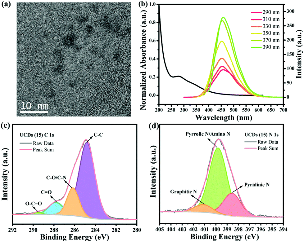 | ||
| Fig. 1 (a) TEM image of the as-prepared CDs; (b) UV-vis spectrum and PL emission spectra at various excitation wavelengths for the as-prepared CDs aqueous solution; (c) C 1s and (d) N 1s core-level spectra of UCDs (15). | ||
The contents of C, N and O were determined to be 53.72%, 15.39% and 30.89%, respectively. The high-resolution XPS spectrum of the C 1s line (Fig. 1c) for the UCDs (15) sample was deconvoluted into five components: C–C (284.8 eV, 68.49%), C–O/C–N (286.2 eV, 19.18%), CO (287.8 eV, 10.96%), O–CO (289.5 eV, 1.37%), suggesting the existence of graphitic, aliphatic, nitrous, and oxygenated C.45 In the case of the N 1s line (Fig. 1d), three types of N species were found, pyridinic N (C–NC, 398.6 eV, 23.29%), pyrrolic N/amino N (C–N–C/N–H, 399.8 eV, 68.49%), and graphitic N (N–(C)3, 401.1 eV, 8.22%),46,47 existing both at the surface and inside the core structure. The presence of different types of N groups have shown to be beneficial for charge-transport properties.48
The deposition of the UCDs onto the FTO was also assessed by SEM and AFM (Fig. S2†), where a homogeneous film could be clearly seen covering the surface of the FTO substrate.
Characterization of H/UCDs photoanodes
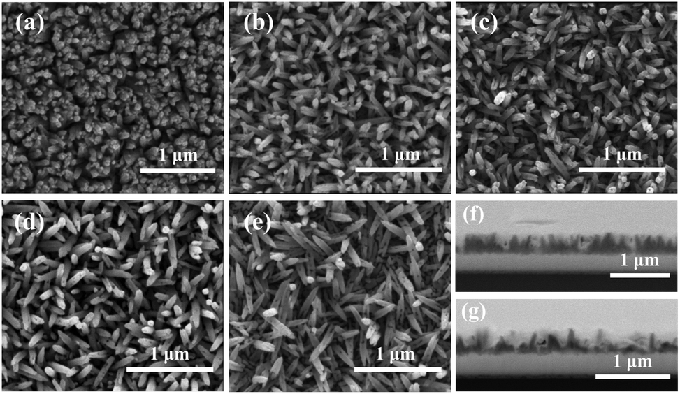 | ||
| Fig. 2 SEM images of (a) pristine hematite, (b) H/UCDs (5), (c) H/UCDs (10), (d) H/UCDs (15), (e) H/UCDs (20); cross-section SEM images of the (f) pristine hematite and (g) H/UCDs (10) photoanodes. | ||
The chemical composition and electronic structure of pristine hematite and H/UCDs (15) photoanodes were studied by HAADF-STEM with EELS mapping (Fig. 3). As expected, the individual C, O, Fe, and combined Fe + O + C RGB EELS mapping images revealed that pristine hematite and the H/UCDs (15) are mostly composed of Fe and O. Although C is observed for both samples, the weak and randomly distributed C signal detected in the pristine hematite is attributed to environmental adventitious carbon as a consequence of being exposed to air (Fig. 3a). In contrast, the strong and more uniform distribution of carbon along the edges of the H/UCDs (15) nanorods (Fig. 3b) suggests that in this case the C comes most likely from the UCDs layer. We believe this C may have been introduced in the hematite via decomposition and volatilization of the carbon underlayer during the transformation of FeOOH into α-Fe2O3 (hematite). The derived C overlayer on hematite is expected to contribute to suppressing surface charge recombination by passivating surface states, thus boosting the photocurrent of hematite photoanodes.25–27
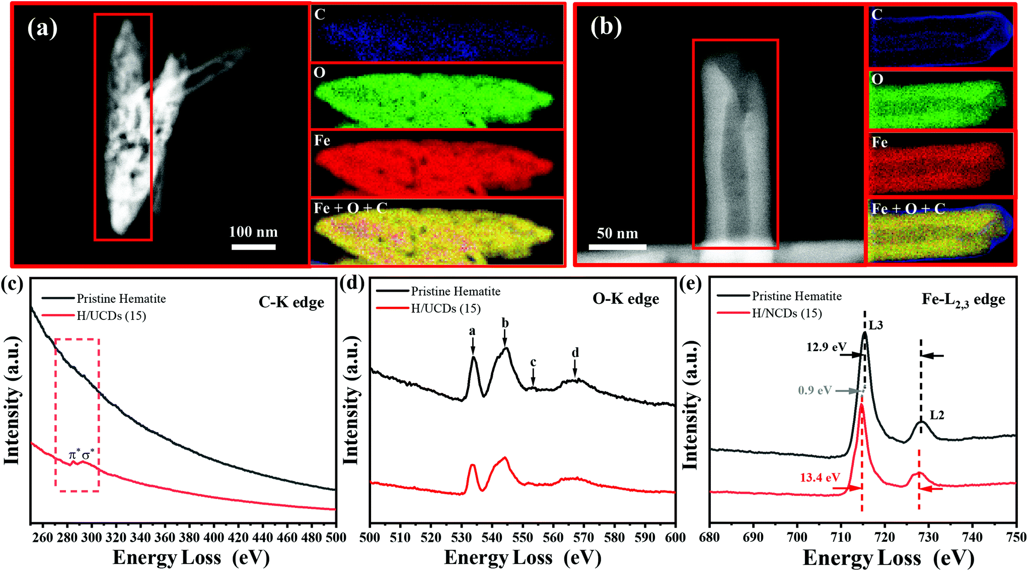 | ||
| Fig. 3 EELS chemical composition maps obtained from the highlighted area in red on the ADF-STEM selected on one of the nanorod from the pristine hematite sample (a) and H/UCDs (15) sample (b); (c) C–K edge, (d) O–K edge, and (e) Fe-L2,3 edge spectrum of the pristine hematite and the H/UCDs (15). | ||
Fig. 3c and d, and e present the corresponding EELS spectra of the C K edge, O K edge, and Fe L2,3 edge for pristine hematite and H/UCDs (15). The corresponding zero-loss peaks of EELS spectrum were provided in Fig. S4.† In the case of the H/UCDs (15), the C signal displays a first peak at 285 eV, induced by π* molecular orbital transitions due to the presence of sp2 bonding, and a second peak at 290 eV induced by transitions to σ* orbitals. In the case of pristine hematite, four peaks (a–d) were identified (Fig. 3d) for the O–K edge signal. Peak a is related to the hybridization of the O 1s to 2p with the Fe 3d orbital, while peak b is associated with the hybridization between the O 2p orbital and the Fe 4s and 4p orbitals. Peaks c and d are caused by the scattering of the third and the first oxygen coordination shells.49–51 There are no significant differences between the O–K edge spectrum of pristine hematite and H/UCDs (15), indicating similar oxygen coordination and electronic environment for both samples. The L edge spectrum of metal cations can be used to probe their ionization state through the analysis of the relative position and intensity of individual L3 and L2 edges.49,51,52 The Fe L3 peak of the H/UCDs (15) exhibited a chemical shift of 0.9 eV toward lower energy compared to that of the pristine hematite (Fig. 3e). The separation between L3 and L2 peaks increases from 12.9 eV for the pristine hematite to 13.4 eV for H/UCD (15). In addition, the intensity ratio of L3/L2 is ca. 5.2 for the H/UCDs (15), whereas the value for pristine hematite is ca. 5.5. These results suggest a change in the ionization state of the Fe in the H/UCDs (15), which has previously been attributed to either partial change in the oxidation state from Fe3+ to Fe2+ due to the Fe–C coordination or the formation of oxygen vacancies.49,51,52 Due to the polaron hopping mechanism in hematite, the existence of Fe2+ could significantly increase the conductivity of the material.53,54
The XPS survey spectra (Fig. S4b†) for pristine hematite and H/UCDs samples indicate that all of the prepared photoanode surfaces consist of Fe, O and C. The presence of C in the XPS spectrum of the pristine hematite is attributed to adventitious carbon contamination. For the Fe 2p XPS line (Fig. 4a), two dominant peaks corresponding to Fe 2p1/2 (∼724.3 eV) and Fe 2p3/2 (∼711.1 eV) are observed, accompanied by their shakeup satellite peaks centered at 718.7 eV and 732.9 eV (Fe 2p1/2, sat and Fe 2p3/2, sat), confirming the presence of Fe3+ as Fe2O3.
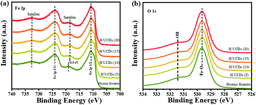 | ||
| Fig. 4 (a) High resolution XPS of Fe 2p line, (b) High resolution XPS of O 1s line for pristine hematite and H/UCDs photoanodes. | ||
55 Importantly, a careful inspection of Fe 2p spectrum reveals that a red shift (0.5 eV) of the Fe 2p1/2 satellite towards lower energy (Fig. 4a) for the H/UCDs samples relative to that of the pristine hematite, suggesting the existence of Fe2+ or Fe–C bonds, which is consistent with the EELS data.56–58 The O 1s spectrum (Fig. 4b) exhibited a main line at 530.0 eV with a shoulder peak at 531.5 eV for all samples, corresponding to the coordination of Fe–O bond and surface hydroxyl species, respectively.55,59
Pristine hematite and H/UCDs show similar optical absorbance edge, from ∼600 to ∼400 nm, indicating the introduction of UCDs does not have a significant effect on the UV-vis absorption range of hematite photoanodes (Fig. S6a†). However, the absorbance intensity for the H/UCDs samples was lower than that of the pristine hematite, this being particularly notable for the H/UCDs (20) sample, which can be explained by the fact that the shortened and obliquely oriented H/UCDs nanorods produce a reduction in the light absorption relative to the thicker and vertically oriented pristine hematite sample, as already predicted from the SEM images of the H/UCDs samples.60 The Tauc plots for an indirect and a direct band gap are shown in Fig. S6b and S6c,† respectively, showed a band gap of around 1.73 eV for the indirect transition and around 1.80 eV for the direct transition with no significant changes among the different samples.
Photoelectrochemical (PEC) performance and mechanism studies
 | ||
| Fig. 5 LSV curves under (a) light and (b) chopped conditions for pristine hematite and H/UCDs photoanodes. (c) Linear fitting of Mott–Schottky plots for hematite and H/UCDs samples. (d) Nyquist plots of hematite and H/UCDs samples at 1.25 v vs. RHE and inset shows the enlarged view of circled area. | ||
The Efb value for the H/UCDs samples shifts to higher potentials, i.e. from 0.43 V vs. RHE for pristine hematite to 0.67 V vs. RHE for H/UCDs (15). This anodic shift of Efb with an increased Nd is unexpected, as an increase in Nd usually yields a negative shift of Efb by raising the Fermi level (Ef) closer to the conduction band (ECB), thus promoting band bending to accelerate the charge separation. This phenomenon has been previously reported for other doping systems with enhanced photocurrents. However, it has not been satisfactorily explained yet.65–67 The Mott–Schottky measurements at different frequencies (3 kHz and 5 kHz), further confirmed these observations (Fig. S8 and Table S2†) and attributed the enhanced PEC performance for the H/UCDs photoanodes to the increased Nd.
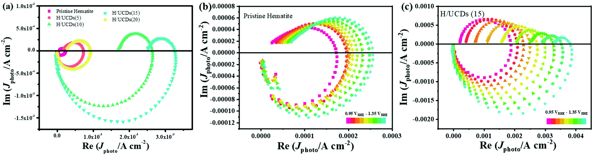 | ||
| Fig. 6 IMPS plots for (a) pristine hematite and H/UCDs photoelectrodes; (b) pristine hematite; (c) H/UCDs (15). | ||
The rate constants, kct (hole transfer rate constant) and krec (surface charge recombination rate constant), the overall charge transfer efficiency (CTE), as well as the diffusion lifetime of the photogenerated electrons carriers (τd) at various potential determined from the IMPS characteristic constants (the frequencies at the minimum and maximum of the semicircles, the low- and high-frequency intercepts) are shown in Fig. 7. Detailed calculation steps can be found elsewhere.68,75 The kct values for all samples (Fig. 7a) increase with increasing potentials. The H/UCDs (10) and H/UCDs (15) exhibit comparable kct values, which are much higher than the rest of the samples. The kct value of H/UCDs (15) at 1.25 V vs. RHE. is almost four times than that of the pristine hematite, indicating an improved hole transfer at its electrode/electrolyte interface. The krec values for H/UCDs (10) and H/UCDs (15) are found decrease with the increase of the potential, whereas the krec values for H/UCDs (5), H/UCDs (20) and hematite remain constant with similar values as a result of Fermi level pinning effects (Fig. 7b). The H/UCDs (10) and H/UCDs (15) samples show a reduced krec compared to that of pristine hematite at potentials above 1.15 V and 1.05 V vs. RHE, respectively. The reduced krec for H/UCDs (10) and H/UCDs (15) indicate a lower surface recombination at the surface state. Note that the H/UCDs (15) has lower krec but similar kct compared to H/UCDs (10). This suggests that the further improved photocurrent of H/UCDs (15) relative to that of H/UCDs (10) is primarily attributed to the decrease in charge recombination. The H/UCDs (20) shows a similar krec as that of the pristine hematite, whereas the H/UCDs (5) exhibits a lower krec. This phenomenon suggests that is the kct, rather than krec, one of the main factors contributing to the increase in photocurrent for the H/UCDs (20). The CTE presented in Fig. 7c further demonstrates the improved charge transfer process for H/UCDs (10) and H/UCDs (15) as a result of their higher kct and lower krec. All the H/UCDs photoelectrodes show a distinct enhancement in τd as compared to the pristine hematite, i.e. the τd of H/UCDs (15) (Fig. 7d). A longer τd means an improved back electron collection and a less recombination during the transfer of electrons to the substrate at the substrate-electrode interface, which allows more holes to be transferred to the electrode surface for water oxidation, hence contributing to the photocurrent enhancement.76 Thus, the IMPS results further reveal that the improved photocurrent for H/UCDs samples is due to the enhanced kct, reduced krec, as well as extended τd.
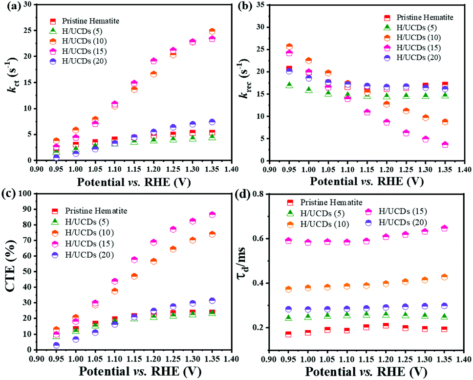 | ||
| Fig. 7 (a) ktr, (b) krec, (c) charge transfer efficiency (CTE), and (d) diffusion lifetime of the photogenerated charge carriers calculated from IMPS plots. | ||
Conclusions
Carbon underlayers produced from biomass – derived carbon dots through a facile hydrothermal process were introduced in hematite photoanodes, in order to enhance the photoresponse of hematite for application in solar-driven water splitting. The formation of this carbon underlayer in combination with a hematite thin film photoelectrode resulted in a remarkable increase in photocurrent density (0.35 mA cm−2 at 1.23 V vs. RHE) compared to pristine hematite. The presence of the carbon underlayer contributes to the back electron collection and transfer, as all the H/UCDs photoelectrodes exhibited longer τd than pristine hematite. Among all the H/UCDs, H/UCDs (15) exhibited the best performance. The promoted back electron collection led to an increase in the carrier concentration in bulk and hole accumulation in surface states for water oxidation. This could be confirmed by the higher Cbulk and Css values of H/UCDs photoelectrodes relative to the pristine hematite.The presence of UCDs also led to the formation of a carbon overlayer via partial decomposition and volatilization of the UCDs during the transformation of FeOOH into hematite, as evidenced by the EELS mapping. The carbon overlayer has been demonstrated to be able to help passivate surface state thus promoting the hole transfer and suppressing charge recombination, which correlates well with the remarkable kct and krec for H/UCDs (10) and H/UCDs (15). Finally, the presence of UCDs and its partial decomposition and volatilization induce the incorporation of C in hematite, resulting in partial change in the oxidation state from Fe3+ to Fe2+ by Fe–C coordination or oxygen vacancy, as indicated by the EELS and XPS analysis. The oxidation state change can improve the bulk conductivity through the polaron hopping mechanism, in good agreement with the improved Nd indicated by Mott–Schottky measurement. This work has shown for the first time a remarkable enhancement of the hematite photocurrent density through the application of a carbon underlayer between FTO and hematite. The triple role of the carbon underlayer that (1) improved the FTO/hematite interfacial properties, (2) provided a carbon source for the formation of an overlayer, and (3) promoted the reduction of some Fe3+ to Fe2+, led to a significant enhancement of bulk and interfacial charge transfer dynamics in hematite, and hence a remarkable improvement in the photoactivity.
Conflicts of interest
There are no conflicts to declare.Acknowledgements
ABJ would like to thank EPSRC (EP/P031323/1) for the financial support. QG and HL acknowledge the CSC scholarship. YF and XW thank the Royal Society for the Advanced Newton Fellowship (NAF\R1\180198), National Natural Science Foundation of China (21703040 and 21861130353) for the financial support. QR acknowledges the UCL Dean's prize and China CSC scholarship. QR and JT acknowledge the financial supports from UK EPSRC (EP/N009533/1) and the Leverhulme Trust (RPG-2017-122). We thank Dr Russell Bayley and Dr Vicente Araullo-Peters for the help of material characterization and the Diamond Light Source for access and support in use of the electron Physical Science Imaging Centre (Instrument E01 proposal MG22447).References
- Q. Ma, Y. Yu, M. Sindoro, A. G. Fane, R. Wang and H. Zhang, Adv. Mater., 2017, 29, 1605361 CrossRef.
- J. Wang, P. Nie, B. Ding, S. Dong, X. Hao, H. Dou and X. Zhang, J. Mater. Chem. A, 2017, 5, 2411–2428 RSC.
- J. Briscoe, A. Marinovic, M. Sevilla, S. Dunn and M. Titirici, Angew. Chem., Int. Ed., 2015, 54, 4463–4468 CrossRef CAS.
- R. Sekiya, Y. Uemura, H. Murakami and T. Haino, Angew. Chem., Int. Ed., 2014, 53, 5619–5623 CrossRef CAS.
- Y. Si, X. Wang, C. Yan, L. Yang, J. Yu and B. Ding, Adv. Mater., 2016, 28, 9512–9518 CrossRef CAS.
- L. Wang, Q. Zhang, S. Chen, F. Xu, S. Chen, J. Jia, H. Tan, H. Hou and Y. Song, Anal. Chem., 2014, 86, 1414–1421 CrossRef CAS.
- Y. Tachibana, L. Vayssieres and J. R. Durrant, Nat. Photonics, 2012, 6, 511 CrossRef CAS.
- M. Grätzel, Nature, 2001, 414, 338 CrossRef.
- A. Fujishima and K. Honda, Nature, 1972, 238, 37 CrossRef CAS.
- X. Yang, A. Wolcott, G. Wang, A. Sobo, R. C. Fitzmorris, F. Qian, J. Z. Zhang and Y. Li, Nano Lett., 2009, 9, 2331–2336 CrossRef CAS.
- A. Kay, I. Cesar and M. Grätzel, J. Am. Chem. Soc., 2006, 128, 15714–15721 CrossRef CAS.
- W. Li, P. Da, Y. Zhang, Y. Wang, X. Lin, X. Gong and G. Zheng, ACS Nano, 2014, 8, 11770–11777 CrossRef CAS.
- T. W. Kim and K.-S. Choi, Science, 2014, 343, 990–994 CrossRef CAS.
- Y. Li, T. Takata, D. Cha, K. Takanabe, T. Minegishi, J. Kubota and K. Domen, Adv. Mater., 2013, 25, 125–131 CrossRef CAS.
- J. Bian, Q. Li, C. Huang, J. Li, Y. Guo, M. Zaw and R.-Q. Zhang, Nano Energy, 2015, 15, 353–361 CrossRef CAS.
- P. Tang, H. Xie, C. Ros, L. Han, M. Biset-Peiro, Y. He, W. Kramer, A. P. Rodriguez, E. Saucedo, J. R. Galan-Mascaros, T. Andreu, J. R. Morante and J. Arbiol, Energy Environ. Sci., 2017, 10, 2124–2136 RSC.
- W. J. Jo, J. W. Jang, K. j. Kong, H. J. Kang, J. Y. Kim, H. Jun, K. Parmar and J. S. Lee, Angew. Chem., Int. Ed., 2012, 51, 3147–3151 CrossRef CAS.
- S. Shen, J. Jiang, P. Guo, C. X. Kronawitter, S. S. Mao and L. Guo, Nano Energy, 2012, 1, 732–741 CrossRef CAS.
- R. Liu, Z. Zheng, J. Spurgeon and X. Yang, Energy Environ. Sci., 2014, 7, 2504–2517 RSC.
- Y. Lin, S. Zhou, S. W. Sheehan and D. Wang, J. Am. Chem. Soc., 2011, 133, 2398–2401 CrossRef CAS.
- T. Hisatomi, H. Dotan, M. Stefik, K. Sivula, A. Rothschild, M. Graetzel and N. Mathews, Adv. Mater., 2012, 24, 2699–2702 CrossRef CAS.
- L. Steier, I. Herraiz-Cardona, S. Gimenez, F. Fabregat-Santiago, J. Bisquert, S. D. Tilley and M. Grätzel, Adv. Funct. Mater., 2014, 24, 7681–7688 CrossRef CAS.
- O. Moradlou, Z. Rabiei, A. Banazadeh, J. Warzywoda and M. Zirak, Appl. Catal., B, 2018, 227, 178–189 CrossRef CAS.
- J. Y. Kim, J.-W. Jang, D. H. Youn, J. Y. Kim, E. S. Kim and J. S. Lee, RSC Adv., 2012, 2, 9415–9422 RSC.
- J. Deng, X. Lv, J. Gao, A. Pu, M. Li, X. Sun and J. Zhong, Energy Environ. Sci., 2013, 6, 1965–1970 RSC.
- T. H. Wang, C.-C. Chiang, Y.-L. Wu, C. Lin, Y.-J. Cheng, Y.-K. Hsieh, C.-F. Wang and C. Huang, Appl. Catal., B, 2017, 207, 1–8 CrossRef CAS.
- M. P. Cardona, M. Li, W. Li, J. McCall, D. Wang, Y. Li and C. Yang, Mater.Today Energy, 2018, 8, 8–14 CrossRef.
- A. Annamalai, A. G. Kannan, S. Y. Lee, D.-W. Kim, S. H. Choi and J. S. Jang, J. Phys. Chem. C, 2015, 119, 19996–20002 CrossRef CAS.
- Y. Liu, W. Li, J. Li, Y. Yang and Q. Chen, RSC Adv., 2014, 4, 3219–3225 RSC.
- Y. Hou, Z. Wen, S. Cui, X. Feng and J. Chen, Nano Lett., 2016, 16, 2268–2277 CrossRef CAS.
- C. X. Guo, Y. Dong, H. B. Yang and C. M. Li, Adv. Energy Mater., 2013, 3, 997–1003 CrossRef CAS.
- Z. Liang, H. Hou, Z. Fang, F. Gao, L. Wang, D. Chen and W. Yang, ACS Appl. Mater. Interfaces, 2019, 11, 19167–19175 CrossRef CAS.
- T.-Y. Yang, H.-Y. Kang, K. Jin, S. Park, J.-H. Lee, U. Sim, H.-Y. Jeong, Y.-C. Joo and K. T. Nam, J. Mater. Chem. A, 2014, 2, 2297–2305 RSC.
- D. Wang, G. Chang, Y. Zhang, J. Chao, J. Yang, S. Su, L. Wang, C. Fan and L. Wang, Nanoscale, 2016, 8, 12697–12701 RSC.
- Z. Luo, T. Wang, J. Zhang, C. Li, H. Li and J. Gong, Angew. Chem., Int. Ed., 2017, 56, 12878–12882 CrossRef CAS.
- F. Le Formal, M. Grätzel and K. Sivula, Adv. Funct. Mater., 2010, 20, 1099–1107 CrossRef CAS.
- O. Zandi, J. A. Beardslee and T. Hamann, J. Phys. Chem. C, 2014, 118, 16494–16503 CrossRef CAS.
- Y. Wang and A. Hu, J. Mater. Chem. C, 2014, 2, 6921–6939 RSC.
- D. Bhattacharya, M. K. Mishra and G. De, J. Phys. Chem. C, 2017, 121, 28106–28116 CrossRef CAS.
- V. Sharma, P. Tiwari and S. M. Mobin, J. Mater. Chem. B, 2017, 5, 8904–8924 RSC.
- S. R. Pendlebury, A. J. Cowan, M. Barroso, K. Sivula, J. Ye, M. Grätzel, D. R. Klug, J. Tang and J. R. Durrant, Energy Environ. Sci., 2012, 5, 6304–6312 RSC.
- K. Sivula, F. Le Formal and M. Grätzel, ChemSusChem, 2011, 4, 432–449 CrossRef CAS.
- P. Anilkumar, X. Wang, L. Cao, S. Sahu, J.-H. Liu, P. Wang, K. Korch, K. N. Tackett Ii, A. Parenzan and Y.-P. Sun, Nanoscale, 2011, 3, 2023–2027 RSC.
- Y. Park, J. Yoo, B. Lim, W. Kwon and S.-W. Rhee, J. Mater. Chem. A, 2016, 4, 11582–11603 RSC.
- L. Lin, X. Song, Y. Chen, M. Rong, T. Zhao, Y. Jiang, Y. Wang and X. Chen, Nanoscale, 2015, 7, 15427–15433 RSC.
- R. Hu, L. Li and W. J. Jin, Carbon, 2017, 111, 133–141 CrossRef CAS.
- C. Hu, C. Yu, M. Li, X. Wang, Q. Dong, G. Wang and J. Qiu, Chem. Commun., 2015, 51, 3419–3422 RSC.
- H. Luo, S. Dimitrov, M. Daboczi, J.-S. Kim, Q. Guo, Y. Fang, M.-A. Stoeckel, P. Samorì, O. Fenwick, A. B. Jorge Sobrido, X. C. Wang and M. Titirici, ACS Appl. Nano Mater., 2020, 3, 3371–3381 CrossRef CAS.
- C. Colliex, T. Manoubi and C. Ortiz, Phys. Rev. B: Condens. Matter Mater. Phys., 1991, 44, 11402 CrossRef CAS.
- C. Wang, Y. Wang, X. Liu, H. Yang, J. Sun, L. Yuan, G. Zhou and F. Rosei, Nanotechnology, 2015, 27, 035702 CrossRef.
- Y. L. Chueh, M. W. Lai, J. Q. Liang, L. J. Chou and Z. L. Wang, Adv. Funct. Mater., 2006, 16, 2243–2251 CrossRef CAS.
- D. K. Mann, J. Xu, N. E. Mordvinova, V. Yannello, Y. Ziouani, N. González-Ballesteros, J. P. Sousa, O. I. Lebedev, Y. V. Kolen'ko and M. Shatruk, Chem. Sci., 2019, 10, 2796–2804 RSC.
- T. Liu, M. Morelli and Y. Li, Photoelectrochemical Solar Cells, 2018 pp. 159–218 Search PubMed.
- Y. Ling, G. Wang, J. Reddy, C. Wang, J. Z. Zhang and Y. Li, Angew. Chem., Int. Ed., 2012, 124, 4150–4155 CrossRef.
- J. Wang, N. H. Perry, L. Guo, L. Vayssieres and H. L. Tuller, ACS Appl. Mater. Interfaces, 2019, 11, 2031–2041 CrossRef CAS.
- M. Omran, T. Fabritius, A. M. Elmahdy, N. A. Abdel-Khalek, M. El-Aref and A. E.-H. Elmanawi, Appl. Surf. Sci., 2015, 345, 127–140 CrossRef CAS.
- H. Zhang, Y. K. Kim, H. Y. Jeong and J. S. Lee, ACS Catal., 2018, 9, 1289–1297 CrossRef.
- H. Zhang, W. Y. Noh, F. Li, J. H. Kim, H. Y. Jeong and J. S. Lee, Adv. Funct. Mater., 2019, 29, 1805737 CrossRef.
- C. Tang, B. Sun, M. Li, J. Zhang, X. Fan, F. Gao, Y. Tong, L. Dong and Y. Li, J. Mater. Chem. A, 2019, 7, 8050–8054 RSC.
- M. Li, Y. Yang, Y. Ling, W. Qiu, F. Wang, T. Liu, Y. Song, X. Liu, P. Fang and Y. Tong, Nano Lett., 2017, 17, 2490–2495 CrossRef CAS.
- Y. Ling, G. Wang, H. Wang, Y. Yang and Y. Li, ChemSusChem, 2014, 7, 848–853 CrossRef CAS.
- K. Sivula, R. Zboril, F. Le Formal, R. Robert, A. Weidenkaff, J. Tucek, J. Frydrych and M. Gratzel, J. Am. Chem. Soc., 2010, 132, 7436–7444 CrossRef CAS.
- R. Morrish, M. Rahman, J. D. MacElroy and C. A. Wolden, ChemSusChem, 2011, 4, 474–479 CrossRef CAS.
- Y. Ling, G. Wang, D. A. Wheeler, J. Z. Zhang and Y. Li, Nano Lett., 2011, 11, 2119–2125 CrossRef CAS.
- K. P. S. Parmar, H. J. Kang, A. Bist, P. Dua, J. S. Jang and J. S. Lee, ChemSusChem, 2012, 5, 1926–1934 CrossRef CAS.
- J. Y. Kim, H. Jun, S. J. Hong, H. G. Kim and J. S. Lee, Int. J. Hydrogen Energy, 2011, 36, 9462–9468 CrossRef CAS.
- F. Malara, A. Minguzzi, M. Marelli, S. Morandi, R. Psaro, V. Dal Santo and A. Naldoni, ACS Catal., 2015, 5, 5292–5300 CrossRef CAS.
- J. Zhang, R. García-Rodríguez, P. Cameron and S. Eslava, Energy Environ. Sci., 2018, 11, 2972–2984 RSC.
- B. Klahr, S. Gimenez, F. Fabregat-Santiago, T. Hamann and J. Bisquert, J. Am. Chem. Soc., 2012, 134, 4294–4302 CrossRef CAS.
- B. Klahr, S. Gimenez, F. Fabregat-Santiago, J. Bisquert and T. W. Hamann, Energy Environ. Sci., 2012, 5, 7626–7636 RSC.
- B. Klahr and T. Hamann, J. Phys. Chem. C, 2014, 118, 10393–10399 CrossRef CAS.
- N. Yatom, O. Neufeld and M. Caspary Toroker, J. Phys. Chem. C, 2015, 119, 24789–24795 CrossRef CAS.
- K. Zhu, N. R. Neale, A. Miedaner and A. J. Frank, Nano Lett., 2007, 7, 69–74 CrossRef CAS.
- D. Monllor-Satoca, M. Bärtsch, C. Fàbrega, A. Genç, S. Reinhard, T. Andreu, J. Arbiol, M. Niederberger and J. R. Morante, Energy Environ. Sci., 2015, 8, 3242–3254 RSC.
- Y. Tang and J. Arbiol, Nanoscale Horiz., 2019, 4, 1256–1276 RSC.
- C. Ding, Z. Wang, J. Shi, T. Yao, A. Li, P. Yan, B. Huang and C. Li, ACS Appl. Mater. Interfaces, 2016, 8, 7086–7091 CrossRef CAS.
- L. M. Peter, L. H. Wong and F. F. Abdi, ACS Appl. Mater. Interfaces, 2017, 9, 41265–41272 CrossRef.
- L. M. Peter, K. U. Wijayantha and A. A. Tahir, Faraday Discuss., 2012, 155, 309–322 RSC.
Footnote |
| † Electronic supplementary information (ESI) available. See DOI: 10.1039/d0nr06139e |
| This journal is © The Royal Society of Chemistry 2020 |