
 Open Access Article
 This Open Access Article is licensed under a
 Creative Commons Attribution 3.0 Unported Licence
Advances in van der Waals thermoelectric materials: prospects and challenges
Marco
Fronzi
 *a,
Paolo
Mele
b,
Amanda V.
Ellis
c and
Catherine
Stampfl
a
*a,
Paolo
Mele
b,
Amanda V.
Ellis
c and
Catherine
Stampfl
a
aSchool of Physics, The University of Sydney, Australia. E-mail: marco.fronzi@sydney.edu.au
bCollege of Engineering, Shibaura Institute of Technology, 307 Fukasaku, Minuma-ku, Saitama 337-8570, Japan
cSchool of Chemical Engineering, University of Melbourne, Australia
First published on 20th March 2025
Abstract
This paper provides a comprehensive review of models and advancements in the discovery of novel van der Waals (vdW) layered materials for thermoelectric applications. The theoretical complexities involved in predicting thermoelectric properties are explored, highlighting the key aspects and challenges in the accurate prediction of fundamental thermoelectric parameters. First-principles and semiclassical models are illustrated, and their respective strengths and limitations in guiding experimental efforts are discussed. The synthesis methods are discussed, suggesting the strengths and limitations of each approach. Current state-of-the-art characterisation techniques for measuring key thermoelectric properties are reported, along with examples of top-performing vdW materials. Critical challenges in developing high-efficiency thermoelectric materials are mentioned, suggesting future research directions.
 Marco Fronzi | Marco Fronzi is a Senior Research Scientist at the School of Physics, University of Sydney, specialising in computational condensed matter physics. He received his PhD from the University of Rome “Tor Vergata”. After his PhD, he was later awarded a Japan Society for the Promotion of Science Fellowship, and he has held research appointments in Japan, Ireland, China and Australia. His scientific interests focus on the application of quantum mechanical, semi-classical and machine learning models to understand and predict the properties of novel materials with technological relevance. His work explores materials for energy conversion applications, including thermoelectric, solar-to-chemical processes, photovoltaics and other energy conversion processes. |
 Paolo Mele | Prof. Paolo Mele is currently a tenured Professor at Shibaura Institute of Technology (Omiya campus, Saitama, Japan). He obtained a Masters degree in Chemistry and a PhD in Chemical Sciences from the University of Genoa (Italy). In 2003, he moved to ISTEC-SRL in Tokyo to study melt-textured ceramic superconductors. He then worked as a postdoc at Kyoto University (JSPS fellowship) from 2004 to 2007, Kyushu Institute of Technology (JST fellowship) from 2007 to 2011, Hiroshima University (as lecturer) from 2011 to 2014, and Muroran Institute of Technology (as Associate Professor) from 2015 to 2018, before reaching his current position. His research interests include materials for energy and sustainable development (superconductors and thermoelectrics); fabrication and characterization of thin films of oxides, ceramics, and metals; study of the effect of nanostructuration on physical properties; thermal transport; vortex matter and the development of new materials for photoelectrocatalysis. Recently, Prof. Mele has focused on the intersection of materials science and computational methods, with a particular emphasis on sustainable energy materials. |
 Amanda V. Ellis | Professor Ellis is the Head of the School of Chemical and Biomedical Engineering at The University of Melbourne, Australia. She graduated from the University of Technology, Sydney in 2003 and has undertaken postdoctoral appointments at Rensselaer Polytechnic Institute, New Mexico State University and Callaghan Innovations, NZ. She has been a Professor and Australian Research Future Fellow at Flinders University, South Australia. Her work focuses on interfacial engineering and chemistries of materials for energy storage/harvesting and device application. |
 Catherine Stampfl | Catherine Stampfl is a Professor in the School of Physics at The University of Sydney working in the area of computational condensed matter physics. She received her PhD from La Trobe University, Australia, and Habilitation from the Technical University, Berlin, Germany. She has worked at the Fritz-Haber-Institute of the Max-Planck Society, Berlin, in the Electronic Materials Laboratory at Xerox Palo Alto Research Center, California, in the Department of Physics and Astronomy, Northwestern University, Evanston Chicago. She has published over 300 papers and is a Fellow of the Australian Academy of Science and the Royal Society of New South Wales. |
I. Introduction
Thermoelectric transformation is a versatile form of energy conversion that efficiently uses the abundant waste heat generated by current industrial processes. This technology is not only advantageous for converting heat into electricity, enabling the recovery of energy that would otherwise be lost through the Seebeck effect, but it is also effective in reverse using electricity to drive cooling processes through the Peltier effect.1,2 These dual capabilities make thermoelectric materials highly valuable for both power generation and cooling applications, offering a sustainable solution to enhance energy efficiency and reduce overall energy consumption in various industries.Recently, the integration of thermoelectric materials in emerging technological areas has been reported. Of particular interest, thermoelectric materials are starting to find their way into artificial intelligence (AI) to implement functionalities such as hand motion recognition3 and robotic hand response.4 Further, they are used in fire alarming systems5 and smart building technologies6 where the conversion of thermal fluctuations into usable electrical signals improves automation and energy efficiency. These materials especially in the 2D van der Waals (vdW) systems have shown rather specific transport characteristics which make them very promising for future electronic and optoelectronic devices.
The thermoelectric conversion efficiency is quantified by the figure of merit, 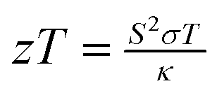 and the power factor PF = S2σ. In this expressions z is a dimensionless coefficient that reflects the material's performance, whereas S is the Seebeck coefficient, which quantifies the voltage generated in response to a temperature difference, σ is the electrical conductivity, T is the absolute temperature, and κ is the thermal conductivity.7 High zT values indicate high efficiency in thermal-to-electrical energy conversion, whereas the power factor (PF) quantifies the ability of a material to generate electrical power from a given temperature gradient.8
Van der Waals (vdW) layered materials have emerged as a promising class of thermoelectric materials.9 Their key feature consists in the low dimensionality of the chemical bonds along the x–y plane, held together by weak van der Waals forces along the perpendicular direction, allowing for easy mechanical exfoliation and the creation of atomically thin layers that can be combined as Lego blocks, offering a huge space of unexplored novel materials with exotic chemical and physical properties.10
The reduced dimensionality and consequent electronic wave-function confinement make this class of materials fundamentally different from their three-dimensional counterparts. Proper engineering of the layers can significantly enhance carrier mobility and reduce lattice thermal conductivity, leading to an increased thermoelectric figure of merit and overall conversion efficiency. These effects on key parameters are driven by quantum confinement, and highlight the potential for optimising thermoelectric properties in two-dimensional materials.11,12
Compared to bulk materials, the quantum confinement and reduced dimensionality in 2D systems can enhance the density of states near the Fermi level, leading to an improved Seebeck coefficient, while phonon scattering at the atomic scale can reduce thermal conductivity, thereby increasing the overall thermoelectric efficiency.
Recent advancements in the synthesis and characterisation of vdW layered materials have opened new avenues for optimising their thermoelectric performance.13 Various methods such as mechanical exfoliation, chemical vapour deposition (CVD), and solution-based techniques have been employed to produce high-quality vdW layers with controlled thickness and composition.10,14,15 Each method offers distinct advantages and challenges in terms of scalability, uniformity, and material quality. For instance, CVD can produce large-area monolayers suitable for practical applications, while solution-based methods offer a scalable route for mass production.16,17
Several layered 2D materials have been experimentally investigated for their thermoelectric performance, with maximised power factors achieved under specific conditions. The key categories of high-performing thermoelectric 2D materials include: transition metal dichalcogenides (TMDs), such as MoS2 and WSe2, which have shown promising results when carrier concentration is tuned through electric double-layer gating; titanium disulphide (TiS2), which exhibits moderate thermoelectric performance when intercalated with organic molecules due to enhanced charge transport; graphene, which, despite its intrinsically low Seebeck coefficient, achieves an exceptional power factor when placed on hexagonal boron nitride (h-BN), benefiting from reduced carrier scattering; and black phosphorus (bP), known for its anisotropic electronic properties, which demonstrates enhanced thermoelectric performance under electrostatic gating.
Table 1 summarises the main categories of layered 2D materials together with the notable features. These findings highlight the tunability of thermoelectric properties in 2D systems and underscore their potential for energy harvesting applications.
| Material family | Notable features |
|---|---|
| Transition metal dichalcogenides (TMDs) | Tunable electronic properties, ranging from semiconducting to metallic behaviours |
| Group IV–VI compounds | Anisotropic crystal structures with high Seebeck coefficients and low thermal conductivity |
| Janus monolayers | Structural asymmetry leads to anisotropic electronic and vibrational properties, resulting in high thermoelectric performance |
| MXenes | Surface functionalization can induce semiconducting properties with good thermoelectric performance |
Despite these advancements, several challenges remain, and achieving high zT values requires a delicate balance between electrical conductivity and thermal conductivity.18 Increasing electrical conductivity often leads to an increase in thermal conductivity, which can be detrimental to thermoelectric performance.8 Therefore, strategies to decouple these properties are critical, and the contribution of defects, grain boundaries, and layer-to-layer interactions plays a significant role.19 Additionally, the integration into functioning devices while maintaining their intrinsic properties is a challenge that needs to be addressed.20
This paper reviews the recent advancements in vdW layered thermoelectric materials, identifies the challenges faced in their development, and explores potential future research directions. We discuss various synthesis methods, the structural and electronic properties of these materials, and their thermoelectric performance. We also highlight recent experimental and theoretical frameworks that have contributed to our understanding of the fundamental mechanisms. By addressing the current challenges and exploring innovative solutions, we aim to provide insights into the future directions of research.
II. vdW layered structures as good thermoelectric materials
Achieving high thermoelectric performance requires optimising several interrelated parameters: the Seebeck coefficient (S), electrical conductivity (σ), and thermal conductivity (κ). The figure of merit, , combines these parameters into a single value that measures overall device efficiency. Increasing S can improve the voltage generated from a temperature gradient, but it often comes at the cost of reducing σ. Similarly, while reducing κ improves heat retention, it can be challenging because increasing σ often leads to a proportional increase in κ. The key to designing high-performance thermoelectric devices is to decouple these parameters, for instance by engineering materials with low lattice thermal conductivity but high electrical conductivity, such as vdW materials. By carefully balancing these parameters, researchers can design materials that perform optimally under real-world conditions. This requires not only an understanding of the material's intrinsic properties but also how these properties translate to device performance in practical applications.
The formulation of these quantities can be expressed as a function of the fundamental physical parameters. The Seebeck coefficient is:
 | (1) |
 | (2) |
Thermal conductivity, with contribution from electron and phonon diffusion (κ = κe + κp), has the general form:
 | (3) |
Here n is the number of particles per unit volume, 〈v〉 is the mean particle speed, λ is the mean free path, cV is molar heat capacity and NA is Avogadro's number.
A low lattice thermal conductivity, high electric conductivity and large Seebeck coefficient are desired to maintain a high zT. The complex inter-correlations between the variables in the definition of each thermoelectric parameter make it difficult to improve all the properties simultaneously.
In general, 2D materials can leverage their low dimensionality to address some of the challenges that make it difficult to simultaneously adjust all variables to a desired target (as schematically illustrated in Fig. 1). The potential benefit can be summarised here:
 | ||
| Fig. 1 a) Schematic trend of normalised properties as a function of carrier concentration for both 3D and 2D materials. The plot shows the behaviour of the Seebeck coefficient (S), electrical conductivity (σ), thermal conductivity (κ), power factor (S2σ), and figure of merit (zT) for carrier concentrations ranging from 1018 to 1022 cm−3. Solid lines represent 3D material properties: S (dark blue), σ (orange), κ (dark green), S2σ (dark red), and zT (red). Dashed and dotted lines represent corresponding 2D material properties: S2D (dark blue, dashed), σ2D (orange, dashed), κ2D (dark green, dashed), S2σ2D (dark red, dash-dotted), and zT2D (red, dash-dotted). The x-axis is logarithmically scaled to show the wide range of carrier concentrations, and the y-axis displays normalised properties with a limit up to 2.5. The legend at the top center provides a clear distinction between 3D and 2D properties for each parameter. b1) Schematic representation of the 2D structural and electronic features that potentially contribute to the shift of the variables in the plot a). Here, b2) represents the two dimensional phonon–phonon scattering, b3) localised phonon modes, as extracted from the work of Sun et al.21 | ||
1. 2D quantum confinement leads to a sharper density of states (g(ε,V)) near the Fermi level, which increases the energy dependence of the electronic states, thus increasing S.11,22 Firstly, the improvement in the Seebeck coefficient in superlattices is generated from the step-like n(ε,V), produced by n(ε,V) = g(ε,V)f, where g(ε,V) is the density of states (DOS) per unit volume and per unit energy. This g(ε,V) can be increased through carrier-pocket engineering in superlattices. When the width of the barrier layer is comparable to that of the quantum well, the localised electron wave function will be released. The anisotropy of the band structure offers a possibility of tuning the relative contributions of different carrier pockets at the Fermi surface by changing the superlattice parameters, such as the growth direction, lattice period, and layer thickness. This leads to a sharp shift in the local DOS and an increment of the Seebeck coefficient with little change in the carrier concentration, thus decoupling the electrical conductivity and the Seebeck coefficient. In doped layers, the presence of ionised impurity scattering centers confined in the potential well and blocked by the potential barrier reduces the carrier scattering events, resulting in higher carrier mobility, which has a slight influence also on phonon transport, leading to μ/κp values of a superlattice being much higher than those of bulk materials.
2. Interface effects can be divided into three categories: specular, diffuse, and hybrid (partially specular and partially diffuse). At a diffuse interface, the thermal conductivity along the layers is irrelevant to the transmissivity and reflectivity. Therefore, the thermophysical properties are decoupled and can be calculated from the individual layers separately.22
3. In the presence of delocalised graphene-like π-electrons, high electrical conductivity can be achieved. Furthermore, the 2D structure reduces scattering events, which increases charge carrier mobility.23 The heat carried by charges during transmission links electrical and electronic thermal conductivity through the Wiedemann–Franz law. Although electric and electronic thermal conductivity are distinct properties, they exhibit similar behaviour at a specific temperature, and essentially the ratio of these conductivities can be approximated to the Lorentz number.24
4. The weak interlayer vdW forces will result in low phonon transport across layers, significantly reducing lattice thermal conductivity.19,25 The phonon mean free path (MFP) is substantially different when comparing 2D and three-dimensional (3D) materials: in 2D materials, phonons are confined to two dimensions, which generally leads to different scattering mechanisms compared to 3D materials.26,27 Phonon–phonon scattering and boundary scattering tend to be more significant in 2D materials because of the increased surface-to-volume ratio. As a general trend, the reduced dimensionality in 2D materials like graphene or transition metal dichalcogenides can lead to longer phonon mean free paths, due to the fewer available scattering channels compared to 3D materials28 In 3D materials, phonons have more available scattering channels due to the higher number of degrees of freedom. This typically results in shorter phonon mean free paths compared to 2D materials.29 Furthermore, 2D superlattices can reduce thermal conductivity upon creation of phonon band gaps and flattened phonon dispersion relations, which limit the group velocity of phonons and enhance scattering, leading to lower thermal transport.30 However, phonon scattering depends on the nature of the specific interface that can be appropriately engineered, and phonon transmission can be either facilitated or hindered. Proper engineering of the interface and the presence of defects, grain boundaries, and interfaces in 2D heterostructures may increase phonon scattering, which disrupts the flow of heat-carrying phonons and reduces thermal conductivity. Furthermore, phonon modes can become localised, which effectively limits thermal conductivity as it reduces the overall phonon transmission across the material.21
5. The quantum-confinement produces a new kind of Umklapp scattering process. The finite layer thickness and the large superlattice constant lead to a small Brillouin zone in the stacking direction. The Umklapp process is confined in this small Brillouin zone, which reduced thermal conductivity. The effect also impacts the thermal conductivity along the layers.
III. Theoretical complexity in thermoelectric properties calculations
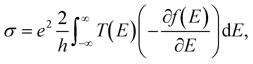
The calculation of thermoelectric parameters requires a detailed understanding of the electronic structure and phonon dynamics within a material.31,32 The Seebeck coefficient, for instance, is a function of the electron density and the transport distribution function, both of which are sensitive to the material's band structure and scattering mechanisms. Similarly, electrical conductivity is governed by the charge carriers' mobility and concentration, which are significantly affected by impurities, defects, and temperature. Thermal conductivity, particularly the lattice contribution, involves complex phonon scattering processes that are difficult to model accurately due to the intricate interactions between phonons, defects, and impurities within the crystal lattice.Within a quantum mechanics framework, the Seebeck coefficient can be reformulated as follows:
 | (4) |
The electrical conductivity in the (σαβ) directions is given by:
 | (5) |
Here, ℏ is the reduced Planck constant, V is the volume of the system, k is the wavevector, indicating the momentum state of an electron, Ĵα, Ĵβ are the current operators in the α and β directions, and ĜR(k, ε), ĜA(k, ε) are the retarded and advanced Green's functions, describing the propagation of electronic states and ε is the energy of the electronic states.
The electronic contribution to the thermal conductivity (κe) is:
 | (6) |
The phonon thermal conductivity (κp) is given by:
 | (7) |
The evaluation of the Seebeck coefficient, electrical conductivity, and thermal conductivities purely from first-principles calculations is challenging due to the complex nature of electron and phonon interactions. These calculations require accurate modelling of quantum states, many-body interactions, and non-equilibrium conditions, all of which are computationally intensive. Additionally, accurately accounting for temperature dependence and scattering processes adds further complexity. The quantum mechanical treatment of these quantities often involves advanced methods such as Greens functions and the Kubo formula, making the computations both resource-intensive and technically demanding.
A. Calculation approaches
Quantum mechanical methods, such as density functional theory (DFT), can provide accurate descriptions of the electronic and phonon structure and the behaviour of atomic systems at 0 K. The choice of the suitable exchange-correlation functional, which may significantly impact the energetics and geometry of the materials, can be complemented by a semi-empirical approach. Among the functionals, the local density approximation (LDA) is computationally efficient and works well for systems with slowly varying electron densities, such as simple metals and semiconductors.33,34 However, it tends to over-bind in 2D materials, leading to inaccurate interlayer distances and poor modelling of van der Waals (vdW) interactions, which are crucial for layered materials like graphene and transition metal dichalcogenides (TMDCs). The generalised gradient approximation (GGA) improves upon the LDA by considering the gradient of the electron density, offering better predictions for a wider range of materials, including molecules, surfaces, and bulk systems.35 The GGA, particularly the PBE functional, is widely used due to its balance between accuracy and computational cost. However, the GGA still underestimates binding energies and overestimates bond lengths in weakly bound systems, leading to possibly large inaccuracies in vdW materials. It also struggles with systems exhibiting strong electron correlation, such as certain TMDCs and complex oxides.35 Meta-GGA functionals, like strongly constrained and appropriately normed (SCAN), capture the delicate balance between covalent and vdW interactions, leading to more accurate modelling of these systems. However, the inclusion of higher-order terms in meta-GGA functionals increases computational complexity, making them more resource-intensive and potentially less consistent across different material types.36 Finally, hybrid functionals, such as B3LYP and HSE06, combine exact Hartree–Fock exchange with GGA or LDA, resulting in the highest accuracy for electronic properties, especially for 2D vdW materials.37 These functionals are effective for calculating accurate band gaps and other electronic properties in semiconductors, insulators, and systems with significant electron correlation. However, hybrid functionals are computationally demanding and their accuracy can be sensitive to the choice of parameters, such as the fraction of Hartree–Fock exchange, which may need to be tailored for specific systems.Additionally, van der Waals functionals must be included in DFT calculations due to the inability of DFT to capture dispersion interactions or long-range correlation effects, which is crucial in 2D materials. These functionals provide a way to incorporate non-local correlations and model weak interlayer interactions.38,39 Recent advancements have reduced the computational cost of vdW functionals, making them more comparable to traditional GGA functionals. This has allowed for their application in larger and more complex systems without significant computational penalties.40 A common issue with vdW functionals is their tendency to either overestimate or underestimate interaction strengths. For example, the original vdW-DF may overestimate long-range forces, while vdW-DF2 might underestimate key coefficients like the C6 term, affecting the accuracy of dispersion energy predictions.38,39 The performance of vdW functionals is closely tied to the choice of exchange functional. For instance, using revPBE in vdW-DF can result in inaccurate binding distances. Alternative exchange functionals, such as optB88, have been developed to improve accuracy, but the optimal choice is still strongly system dependent, and there is currently no vdW functional that performs consistently across different materials.38,39
Although the DFT models provide a detailed understanding of electronic structure, calculating thermoelectric parameters requires an additional theoretical framework to describe and quantify transport mechanisms.
The Boltzmann transport equation (BTE) is a common model used to approximate the theoretical value of these properties, within a semi-classical framework.41,42 Solving the BTE requires detailed knowledge of the relaxation times, which are influenced by various scattering mechanisms, including phonon–phonon, electron–phonon, and impurity scattering. Accurately determining these relaxation times often necessitates sophisticated computational techniques, such as ab initio molecular dynamics simulations, which can be computationally expensive and complex.43–45 Moreover, the interplay between electronic and thermal transport properties adds another layer of complexity.46 For instance, strategies to reduce thermal conductivity, such as introducing nano-structures or alloying, can adversely affect the electrical conductivity and the Seebeck coefficient. This interdependence means that theoretical models must simultaneously account for multiple transport phenomena and their interactions, making accurate predictions particularly challenging. For example, the phonon BTE describes thermal transport in a solid where phonons govern the process through vibrations of the crystal's atoms, and any alteration in these vibrations can significantly impact the thermal and electrical transport properties.47,48 Additionally, the relaxation time approximation simplifies the BTE by assuming that all scattering processes can be characterised by a single relaxation time, which is not always valid. This approximation is often used in conjunction with the Wigner–Boltzmann transport equation for systems with homogeneously distributed defects and under the assumption of a linear response to external electric fields.49,50
Within the semi-classical BTE approximations, the formulation of the Seebeck coefficient can be redefined as:51–53
 | (8) |
The integration over all possible energy states, accounting for the distribution of carriers and their energy-dependent transport properties, which are influenced by the material's electronic structure and various scattering mechanisms, makes the calculation of S relatively complex.
The electron conductivity is then given by:
 | (9) |
The integral requires precise knowledge of the energy-dependent transport distribution function and how the carrier distribution changes with energy, making it necessary to consider detailed interactions within the material.
The thermal conductivity in the context of electronic contributions (often denoted as κe) can be expressed quantum mechanically as:
 | (10) |
This expression is complex because it involves two integrals, one of which is included in σS2T, that account for the energy distribution of carriers and their transport properties. In particular, the second term (σS2T) accounts for the correlation between energy levels, adding further complexity to the calculations. An example of calculated S, σ and power factor (PF) within the BTE model is shown in Fig. 2.
 | ||
| Fig. 2 Seebeck coefficient (first row), electrical conductivity (second row) and power factor (third row) of selected vdW heterostructures under strain, calculated within the BTE model by Ahmad et al.54 | ||
The Landauer transport equations (LTE) provide an alternative model to understand electronic transport, particularly at the nanoscale. Unlike the BTE, Landauer theory models conductance as a quantum mechanical transmission problem.55–57 It assumes ballistic transport, where electrons traverse the material without scattering, making it ideal for analysing transport in mesoscopic systems like quantum dots and nanowires.58 While the BTE excels in describing diffusive transport where scattering is significant, Landauer theory gives a more accurate description in systems where quantum coherence is maintained over the length of the conductor. The Landauer approach is particularly useful in systems where quantum effects are non-negligible and where ballistic transport dominates, like low dimensional materials, offering a powerful alternative to the semi-classical nature of the BTE.59 Within the Landauer model the Seebeck coefficient, electron conductivity and electronic thermal conductivity become:51,60
 | (11) |
 | (12) |
 | (13) |
The Landauer formalism focuses on quantum mechanical aspects, particularly the transmission function that reflects the probability of carriers traversing a conductor. It is best suited for mesoscopic systems where phase coherence is crucial, whereas Boltzmann approximation relies on semiclassical assumptions, with a focus on scattering events, relaxation times, and velocities of carriers. It is more applicable to bulk materials where quantum coherence is not significant. Examples of the calculated electronic transmission, Seebeck coefficient, power factor, and thermoelectric figure of merit are shown in Fig. 3.
 | ||
| Fig. 3 Electronic transmission, Seebeck coefficient, power factor, and thermoelectric figure of merit are plotted around the Fermi level for a) 2H-ZrSe2, b) 2H-ZrTe2, c) 2H-HfS2, and d) 2H-HfSe2 using the LTE model.61 | ||
Both approaches are essential for comprehensively understanding transport phenomena, with Landauer theory providing a more straightforward, albeit idealised, perspective compared to the more complex, scattering-based BTE.62
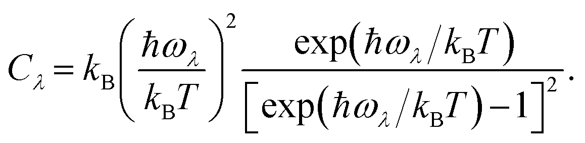
To evaluate the main contribution to thermal conductivity in semiconductors and insulators it is essential to analyse the underlying phonon dynamics, which still involves solving the transport equations, and can be approached using methods like the discrete ordinates method or spherical harmonics expansions. All these methods aim to solve the transport equations numerically, considering anisotropic relaxation times and accounting for phonon–phonon interactions.63–67 The phonon thermal conductivity quantified using lattice dynamics calculations is given by:
 | (14) |
 | (15) |
Here, N is the number of unit cells, Vc the volume of the unit cell, Cλ the mode heat capacity, vλ the phonon group velocity, τSMRTλ the single-mode relaxation time, ℏ the reduced Planck's constant, ωλ the phonon frequency, and nλ(T) the Bose–Einstein distribution function. Complexity arises from the need to integrate over all phonon frequencies and account for the frequency-dependent specific heat, phonon group velocity, and mean free path, which all depend on the intricate details of the lattice dynamics.
In nano-structures and low dimensional systems like quantum wells and superlattices, electron–phonon interactions can lead to non-equilibrium phonon distributions, and should be included for an accurate analysis.68–71
IV. Synthesis methods
Although the experimental measurement of thermoelectric properties requires well-established techniques, the fabrication of 2-dimensional vdW materials requires particular expertise due to the relative novelty of their synthesis and handling methods. The synthesis of 2D layered materials is typically achieved by employing mechanical exfoliation, chemical vapour deposition (CVD), and solution-based techniques.Mechanical exfoliation, also known as the “scotch tape” method, while effective for producing high-quality monolayers, faces challenges in scalability.10 Innovations in automated mechanical exfoliation systems have improved throughput and consistency, making the technique more practical for research applications.23 Detailed steps of this method are discussed in the following section.
CVD has emerged as a key technique for synthesising large-area, high-quality monolayers and heterostructures with precise control over layer thickness and composition. For example, CVD-grown monolayer MoS2 using sulphur and molybdenum hexacarbonyl precursors demonstrates high uniformity and excellent electronic properties, making it suitable for various electronic and optoelectronic applications.14 Additionally, the CVD synthesis of large-area graphene and transition metal dichalcogenides (TMDs) has facilitated the development of high-performance transistors and photodetectors.16
Solution-based methods, including liquid-phase exfoliation and chemical synthesis, offer scalable routes for producing large quantities of vdW materials. These methods involve dispersing bulk crystals in solvents followed by exfoliation through sonication or chemical reactions. The scalability and simplicity of solution-based methods make them attractive for industrial applications, despite challenges in achieving uniformity and controlling defects.15
A. Mechanical exfoliation
The mechanical exfoliation process has been a pioneering technique for isolating monolayers from bulk vdW layered materials. This method involves peeling layers from a bulk crystal using adhesive tape, which are then transferred onto a substrate. Its simplicity and effectiveness in producing high-quality monolayers made it popular in early studies of graphene and other 2D materials.10 However, despite its success in research applications, mechanical exfoliation faces significant limitations in scalability and reproducibility.The process of mechanical exfoliation typically involves several steps:
1. Preparation of bulk crystal: a bulk vdW crystal is cleaved to expose a fresh surface. This initial step is crucial as it ensures that the layers to be exfoliated are clean and free from contaminants, which can otherwise affect the quality of the exfoliated layers.10,23
2. Adhesive application: adhesive tape is applied to the cleaved surface and then peeled away, capturing thin layers of the material. This method has been successfully used to exfoliate a variety of vdW materials, including graphene, MoS2, and other transition metal dichalcogenides (TMDs).72,73
3. Transfer to substrate: the tape with exfoliated layers is pressed onto a substrate, such as silicon dioxide (SiO2) on silicon (Si), and then carefully removed to leave behind the 2D layers. This transfer step is critical to achieving well-aligned and defect-free monolayers.74
Several advancements have been made to refine this technique. For instance, using micro-trench structures has enabled the exfoliation of materials like bismuth to sub-10 nm thicknesses, which can then be analysed using atomic force microscopy and Raman spectroscopy.75 Similarly, mechanical exfoliation has been employed to produce high-mobility layers of GdTe3.76
One of the significant achievements with this method is the ability to produce heterostructures in a relatively easy way.73 Additionally, this method has facilitated the analysis of electronic properties of new materials, such as one-dimensional wires and molecular wires, which are identified through photoluminescence during exfoliation.77 As shown in Fig. 4, the mechanisms and properties of MoS2/metal Schottky junctions illustrate the potential for enabling monolayer-selective mechanical modulation etching (MME).
 | ||
| Fig. 4 A) Simplified schematic of the MoS2/metal Schottky junction illustrating reduced interlayer energy and van der Waals (vdW) interactions. The Schottky-induced electric field distorts the electron distribution, increasing the effective interlayer distance (D) and thereby reducing vdW interactions. Electron depletion (reduced electron density ne) leads to decreased polarisability, further diminishing vdW interactions. B) Electrostatic profile of the MoS2/metal Schottky junction using the full depletion approximation. The electron density ne (green dashed line) decreases in MoS2 (right side) and correspondingly increases in the metal (left side). An electric field (blue dashed line) is established within the MoS2 depletion width (xd), peaking near the interface. The y-axis represents the change in electron density (Δne) or electric field strength, and the x-axis denotes the distance from the interface, with x = 0 at the MoS2/metal interfacial plane. C) Comparison of properties of monolayer MoS2/metal interfaces predicted to enable monolayer-selective MME and experimental attempts with different monolayer MoS2/metal interfaces. Aluminium (Al) could not enable monolayer-selective MME, similar to other reports.78 | ||
Despite its effectiveness in producing high-quality monolayers, mechanical exfoliation is not suitable for large-scale production. The layers obtained can vary in thickness and size, and the process is labor-intensive. For instance, the process typically follows a geometric progression in thickness reduction, rather than a simple halving with each tear, which complicates consistency.79 Advances in automated mechanical exfoliation systems have been made to improve throughput and consistency, but these systems still struggle to meet the demands of industrial applications.80
To address these challenges, research has been directed towards enhancing the reproducibility and scalability of the technique. This includes developing automated systems for layer-by-layer exfoliation and transfer, as well as combining mechanical exfoliation with other techniques like CVD to produce hybrid structures with improved properties.81
While mechanical exfoliation remains a valuable technique for fundamental research and the production of high-quality vdW monolayers, its scalability and consistency challenges need to be addressed to meet the demands of industrial applications. Ongoing research and technological advancements are expected to enhance its practicality and expand its applications in various fields.
B. Chemical vapour deposition
Chemical vapour deposition is a widely used technique for the controlled growth of large-area vdW layers, making it crucial for practical applications. CVD involves the chemical reaction of vapour-phase precursors on a heated substrate, resulting in the deposition of thin films. This method offers precise control over the thickness, composition, and uniformity of the deposited layers, which is essential for high-quality applications.The CVD process typically includes the following steps:
1. Precursor introduction: gaseous precursors are introduced into a reaction chamber containing the substrate. This step is critical as the choice of precursors and their flow rates determine the chemical reactions that will form the vdW layers.82,83
2. Reaction and deposition: the precursors decompose or react at elevated temperatures, leading to the deposition of the desired material on the substrate. For example, in the CVD growth of MoS2, sulphur and molybdenum hexacarbonyl are commonly used precursors.83
3. Post-deposition treatments: annealing or other treatments may be applied to improve crystallinity and remove impurities. These treatments can significantly enhance the electrical and thermal properties of the deposited layers.84,85
CVD has been successfully employed to synthesise a variety of vdW layered materials, including graphene and transition metal dichalcogenides. This method allows the synthesis of large-area monolayers, with satisfactory results for MoS2, highlighting the potential of CVD for reaching industrial level production.83
Additionally, CVD is suitable for the growth of complex vdW heterostructures. The layer-controlled CVD growth of MoS2 vertical heterostructures via vdW epitaxy has shown precise control over the number of layers.83 The development of air-stable 2D magnetic CrS2 on a mica substrate using CVD is another significant advancement, offering new possibilities for magnetic applications at room temperature.85 As illustrated in Fig. 5, the nucleation and growth dynamics of graphene on liquid copper (Cu) are significantly influenced by temperature and precursor concentration under low carbon chemical potential.
 | ||
| Fig. 5 a) Schematic illustration of graphene nucleation on liquid Cu under low carbon chemical potential facilitated by abundant free electrons. b) Plots of the nucleation density and nucleation time of graphene on Cu as functions of temperature. The Arrhenius plot for the nucleation density indicates the activation energies for solid and liquid Cu. c–e) Scanning electron microscopy (SEM) images showing the time evolution of graphene single crystal growth on liquid Cu at 1120 °C with 5 sccm of CH4 for: c) t = 2 s, d) t = 3 s, and e) t = 4 s. Time zero (t = 0 s) is defined as the moment when CH4 is introduced into the CVD furnace. f) and g) Graphene growth conducted at different precursor concentrations of CH4: f) 5 sccm and g) 10 sccm at 1100 for 10 s.86 | ||
However, challenges remain in optimising the CVD process for different materials and ensuring scalability. Achieving uniformity over large areas, controlling the number of layers, and integrating CVD-grown materials with other processes are ongoing areas of research. For example, the anomalous thickness dependence of the Curie temperature for 1 T-CrTe2 grown by CVD shows that more work is needed to understand and control these properties.87 Furthermore, the fabrication of top-gated field-effect transistors (FETs) using CVD-grown materials highlights the need for low-temperature synthesis methods compatible with flexible substrates like glass.88 The synthesis of GaSe/MoSe2 misfit heterostructures using a two-step CVD process demonstrates the ability to create vertically stacked and lateral heterostructures with tunable electronic properties.89
Other important aspects are the vdW structures' surface energy and wettability, which are influenced by the underlying substrate and the dominant vdW forces, and play a crucial role in the overall performance and integration of the materials in devices.90
The synthesis of hexagonal boron nitride (hBN) heterostructures for 2D vdW electronics via CVD is another example of the method's versatility. hBN serves as an excellent insulator and is essential in constructing versatile tunnelling devices.91 Additionally, studies on the thermal conductivity of CVD-grown Bi2O3Se were particularly successful.92
While CVD remains a cornerstone technique for high-quality synthesis, ongoing research is essential to overcome current challenges and improve scalability, uniformity, and integration. Advances in this area will continue to expand the applications of vdW materials in various fields, including electronics, photonics, and thermoelectrics.14,16,82–85,87–96
C. Solution-based methods
Solution-based methods, including liquid-phase exfoliation and chemical synthesis, provide an alternative approach for the large-scale production of vdW layered materials. These methods involve dispersing bulk crystals in a solvent, followed by exfoliation through sonication or chemical reactions to produce monolayers or few-layer nano-sheets.The key steps in solution-based methods are:
1. Dispersion: bulk vdW materials are dispersed in a suitable solvent, often with the aid of surfactants to stabilise the exfoliated layers. For example, surfactants like sodium dodecyl sulphate (SDS) or organic solvents such as N-methyl-2-pyrrolidone (NMP) can be used to facilitate the dispersion of materials like graphene and MoS2.15
2. Exfoliation: ultrasonication or chemical reactions are employed to exfoliate the material into individual layers or nano-sheets. Ultrasonication involves applying high-frequency sound waves to break the vdW interactions holding the layers together. This method has been effective in producing large quantities of few-layer graphene and other 2D materials.15,17
3. Centrifugation: the dispersion is centrifuged to separate the exfoliated layers from the unexfoliated bulk material and other impurities. Centrifugation parameters such as speed and duration are critical in achieving effective separation. High-speed centrifugation helps in isolating monolayers and few-layer nano-sheets from thicker flakes.17
4. Collection: the supernatant containing the exfoliated layers is collected for further processing or use. The quality of the collected material can be further enhanced through additional purification steps, such as filtering or further centrifugation.97
As illustrated in Fig. 6, isopycnic density gradient ultracentrifugation (iDGU) enables layer-by-layer separation of various two-dimensional materials, leading to improved thickness monodispersity. Liquid-phase exfoliation is advantageous due to its simplicity, scalability, and ability to produce large quantities of material. It has been successfully used to exfoliate a wide range of vdW materials, including graphene, transition metal dichalcogenides (TMDs), and black phosphorus. For instance, black phosphorus nano-sheets with high carrier mobility have been produced using liquid-phase exfoliation.15
 | ||
| Fig. 6 Separation by isopycnic density gradient ultracentrifugation (iDGU). a) Layer-by-layer separation of graphene via iDGU. Atomic force microscopy images and cross-sectional line profiles reveal nano-sheets of monolayer and bilayer thickness. b) Layer-by-layer separation of hexagonal boron nitride (h-BN) using iDGU. c–f) Layer-by-layer separation of transition metal dichalcogenides (TMDs) by iDGU with polymeric surfactants reducing the effective buoyant density: c) MoS2, d) WS2, e) MoSe2, and f) WSe2. g) Separation of high-density ReS2 layers using iDGU with a mixture of iodixanol and CsCl to increase the gradient medium's buoyant density. h–j) Thickness histograms demonstrating improved monodispersity after iDGU for h) graphene, i) h-BN, and j) MoS2.98 | ||
Chemical synthesis approaches, such as solvothermal or hydrothermal methods, can also produce vdW materials with controlled morphology and size. These methods involve the reaction of precursors in a solvent at elevated temperatures and pressures, leading to the formation of vdW materials. Solvothermal synthesis has been used to produce MoS2 nano-sheets with precise control over size and morphology.17 However, these methods often result in materials with defects and varying layer thicknesses, which can impact their performance. Defects such as vacancies, grain boundaries, and functional groups introduced during exfoliation can affect the electrical and thermal conductivity of the materials. Efforts to improve the quality and uniformity of solution-processed vdW materials are ongoing, with significant progress being made through the optimisation of exfoliation conditions and the development of novel solvents and stabilisers.99 For instance, optimising the sonication power and duration can help in reducing defects and achieving a higher yield of monolayer materials. Similarly, using high-purity solvents and surfactants can minimise contamination and improve the overall quality of the exfoliated materials. The use of mixed solvents and surfactant combinations to enhance exfoliation efficiency and material quality has also been explored.15
While solution-based methods offer a scalable and versatile approach for producing vdW layered materials, ongoing research is essential to address the challenges related to material quality and uniformity.15,17,97,99
D. Challenges in scaling synthesis for industrial applications
While laboratory techniques like mechanical exfoliation and CVD provide excellent control over material properties at small scales, scaling these methods for industrial applications presents significant challenges. Mechanical exfoliation is highly effective for producing high-quality monolayers but is labor-intensive and difficult to scale for large-scale manufacturing. Conversely, CVD offers scalability but often introduces grain boundaries and non-uniformities that degrade the material's thermoelectric performance.To address these issues, hybrid approaches are being explored, combining CVD with solution-based methods to improve scalability while maintaining high material quality. Automated mechanical exfoliation techniques and innovations in CVD growth parameters are also being developed to bridge the gap between research-grade and industrial-scale production of vdW materials. Overcoming these scaling challenges is critical for translating promising lab-scale materials into commercially viable thermoelectric devices.100,101
V. Characterisation and measurement of relevant thermoelectric properties
While synthesis methods control the structural and electronic properties of vdW materials, characterisation techniques provide valuable feedback to optimise synthesis protocols, understanding the materials' performance and optimising them for applications in commercial devices. They involve evaluating key parameters S, σ and κ. Advanced techniques have been developed to accurately measure these properties in low-dimensional and nano-structured materials.For the Seebeck coefficient, micro-fabricated heater and sensor arrays allow for high-resolution measurements even in small and thin samples. The four-probe method is commonly used to measure electrical conductivity, minimising the effects of contact resistance. Thermal conductivity is measured using techniques such as the 3-omega method, time-domain thermoreflectance (TDTR), and Raman thermometry, each providing insights into the lattice and electronic contributions to thermal transport.
Hall effect measurements are essential for determining carrier concentration and mobility, which directly impact thermoelectric performance. These measurements have been refined to account for the unique properties of vdW materials, enabling accurate assessment of their potential for thermoelectric applications.
The Seebeck coefficient is typically measured using a setup where a temperature gradient is applied across a sample, and the resulting voltage difference is measured.
The Seebeck coefficient can be measured as:
 | (16) |
High-resolution measurements of the Seebeck coefficient in vdW materials can be achieved using micro-fabricated heater and sensor arrays. These arrays allow for localised heating and accurate measurement of the temperature gradient and voltage, even in small and thin samples such as monolayers of TMDs.102
Electrical conductivity is typically measured using a four-probe method to eliminate the effects of contact resistance. In the four-probe method, four electrodes are placed on the sample. A known current is passed through the outer two electrodes, and the voltage drop is measured across the inner two electrodes. The electrical conductivity is then calculated using the formula:
 | (17) |
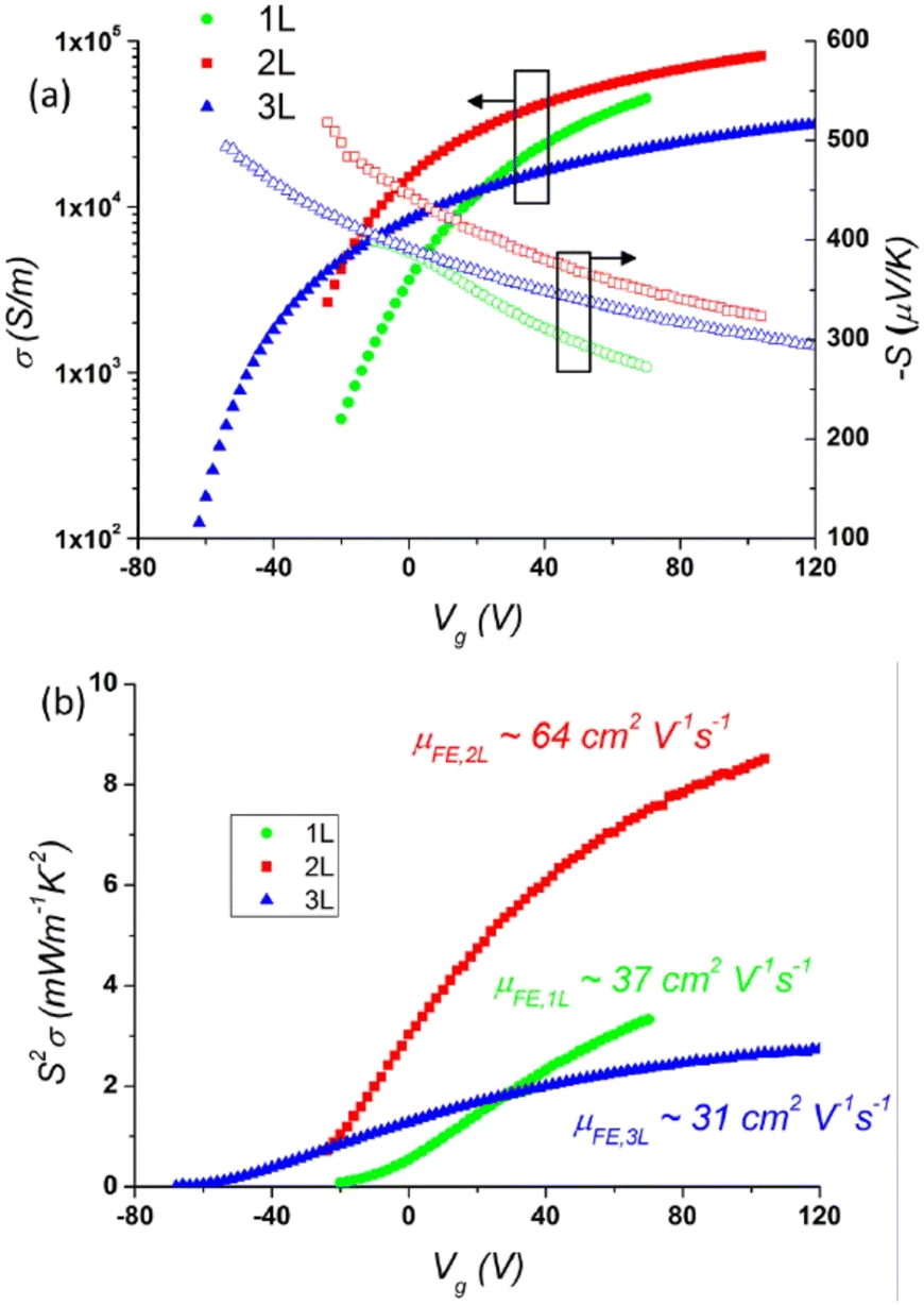 | ||
| Fig. 7 Thermoelectric characterisation of monolayer MoS2, obtained by mechanical exfoliation, at room temperature. Measurements include the Seebeck coefficient (a), electrical conductivity (a), and power factor (b) as functions of carrier concentration, where Vg is the applied gate voltage.104 | ||
Thermal conductivity (κ) is typically measured using a range of options, including the 3-omega method, time-domain thermoreflectance (TDTR), and Raman thermometry.
The 3-omega method involves applying an alternating current at frequency ω through a metal heater line deposited on the sample. The resulting temperature oscillations at frequency 2ω induce a voltage response at frequency 3ω, which can be measured, as schematically illustrated in Fig. 8. The thermal conductivity is then extracted from the phase and amplitude of the 3-omega signal.105 The method's insensitivity to both in-plane and cross-plane thermal conductivity is a limitation.
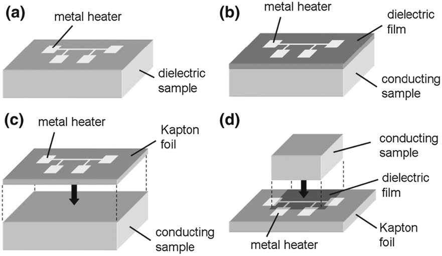 | ||
| Fig. 8 Schematic illustration of the 3-omega method. a) A metal heater strip can be directly deposited on a dielectric sample. b) For electrically conductive samples, an additional dielectric layer is needed between the sample and the heater strip. c) The 3-omega sensor can be prefabricated on a standalone Kapton foil, allowing the same sensor to be used across multiple samples. d) An electrically conductive sample can also be placed on top of the prefabricated sensor if a dielectric layer is added to the heater strip.106 | ||
TDTR is a pump-probe technique where a short laser pulse (pump) heats the sample surface, and a time-delayed probe pulse measures the resulting temperature change by monitoring the reflectance change. The thermal conductivity is determined by analysing the heat flow dynamics in the sample.107 However, the main limitation of this method is its scarce suitability for 2D materials. It requires a minimum sample thickness of 20 nm to measure thermal properties, leading to cross-plane heat transport, which differs significantly from in-plane transport in 2D materials due to weak interlayer coupling. For example, Jiang et al. found a two-order magnitude difference between in-plane and cross-plane thermal conductivities in MX2 (M = Mo, W and X = S, Se) bulk crystals.108 Additionally, the method's costly and highly specialised setup limits its accessibility. A schematic representation is shown in Fig. 9.
 | ||
| Fig. 9 a) Diagram illustrating the experimental setup for the TDTR technique. EOM, PBS, and BS represent the electro-optic modulator, polarising beam splitter, and beam splitter, respectively. b) Diagram demonstrating the elliptical-beam method applied to the sample. c) Depiction of heat flux directions and the comparison between the laser spot size and sample thickness.108 | ||
Raman thermometry uses the temperature dependence of Raman peak positions to measure thermal conductivity. By analysing the shift in Raman spectra with applied heating, the thermal conductivity of the material can be inferred. This method is particularly useful for thin films and nano-structures where traditional methods may be challenging to apply.109 The setup and measurements are illustrated in Fig. 10.
 | ||
| Fig. 10 Laser heating experiment and thermal model: a) schematic of the sample structure and measurement setup, highlighting the thermal boundary resistance (1/thermal boundary conductance) at the MoS2/SiO2 interface. b) Simulated temperature rise during laser heating using a 2D axis symmetric finite element model. c) Normalised power density and temperature rise in the MoS2 film as a function of the radial coordinate for G = 15 MW m−2 K−1 and thermal conductivity k2D = 100 W m−1 K−1, showing a small thermal healing length (LH ∼ 80 nm) compared to the laser beam size (r0 ∼ 300 nm), which leads to insensitivity to the thermal conductivity of the 2D material.110 | ||
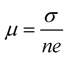
Hall effect measurements, illustrated in Fig. 11, are used to determine the carrier concentration and mobility in thermoelectric materials. In this method, a magnetic field is applied perpendicular to the current flow in the sample, and the resulting Hall voltage is measured. The carrier concentration (n) and mobility (μ) can be calculated using the relations:
 | (18) |
 | (19) |
 | ||
| Fig. 11 Illustration of Hall effects: a) the valley Hall effect occurs in non-magnetic quantum materials like gapped graphene and transition metal dichalcogenides, where the Berry curvature is locked to the K and K′ valleys, causing electrons in opposite valleys to deflect in opposite directions. b) The layer Hall effect is observed in even-layered MnBi2Te4 in the antiferromagnetic topological insulator state, where the Berry curvature is locked to the top and bottom layers, resulting in electrons deflecting in opposite directions in these layers. c) Schematic of dual-gated devices with VBG (bottom gate voltage) and VTG (top gate voltage). d) Longitudinal resistance Rxx as a function of temperature (T) and magnetic field (B), indicating magnetic states: AFM (antiferromagnetic), FM (ferromagnetic), SF (spin-flop), and PM (permanent magnet). (e and f) Rxx and Ryx as functions of VBG in the antiferromagnetic phase at B = 2 T, with CNP (charge-neutral point).111 | ||
A precise characterisation of thermoelectric properties is required for the development and optimisation of novel vdW layered materials. Advanced measurement techniques tailored to the unique properties of these materials have significantly enhanced our understanding and ability to improve their performance.
VI. Thermoelectric 2D layered vdW materials
In this section, we discuss key 2D van der Waals materials and their measured and/or calculated thermoelectric performances, as summarised in Table 2.| Material | Type | Seebeck coefficient (μV K−1) | Power factor (μW m−1 K−2) | Notable features |
|---|---|---|---|---|
| Graphene-based materials | ||||
| Graphene | SL (Exp) | ∼80 (p-doped) | 6600 (holes), 6100 (electrons) | High thermal conductivity (4000 W m−1 K−1) |
| Graphene | ML (Exp) | >100 | 4800 (holes), 4100 (electrons) | Enhanced by heterostructures |
| Graphene/hBN | Heterostructure (Exp) | 182 | 36![[thin space (1/6-em)]](https://www.rsc.org/images/entities/char_2009.gif) 600 (holes), 19000 (electrons) 600 (holes), 19000 (electrons) |
Reduced scattering, higher carrier mobility |
| Graphene/SiO2 | Heterostructure (Exp) | 109 | — | Lower performance compared to hBN substrates |
| Graphene/MoS2 | Heterostructure (Exp) | — | High | Synergy between graphene's conductivity and MoS2's Seebeck |
| Phosphorene-based materials | ||||
|---|---|---|---|---|
| Black phosphorus | ML (Exp) | 77–400 | Up to 500 | Highly anisotropic, tunable via thickness/doping |
| Exfoliated phosphorene | ML (Exp) | — | 200 | High power factor in thin layers (10–30 nm) |
| Ionic-liquid-gated phosphorene | ML (Exp) | — | 500 | Enhanced via electrostatic gating |
| Au-decorated phosphorene | ML (Exp) | 50–400 | 65 | Tunable via Au nanoparticle content |
| MoS2 and WSe2 family | ||||
|---|---|---|---|---|
| MoS2 | SL (Exp) | 10000 |
200 (single layer), 8500 (bilayer) | High carrier mobility, quantum size effects |
| WSe2 | ML (Exp) | 250 (n-type), 380 (p-type) | 3000 | Gate-induced doping enhances performance |
| MoS2 | SL (DFT) | 200 | 8 | Predictions with spin–orbit coupling effects |
| MoS2 | SL (DFT) | — | N × 000 | Band edge gradients enhance zT |
| MoS2/WSe2 | Heterostructure (Exp) | 10000 (MoS2), 380 (WSe2) |
8500 | Synergistic effects enhance performance |
| hBN/MoS2/WSe2 | Heterostructure (Exp) | — | — | Synergistic effects improve thermoelectric efficiency |
| PtSe2 and PtTe2 materials | ||||
|---|---|---|---|---|
| PtSe2 | ML (Exp) | 188 | — | Semi-metallic nature improves Seebeck coefficient |
| PtTe2 | ML (Exp) | — | — | Metallic behavior |
| Oxide-based materials | ||||
|---|---|---|---|---|
| SrTiO3 | Bulk (Exp) | 108 | 0.1 (zT at 300 K) | Enhanced via 2D heterostructures |
| Nb-doped SrTiO3 | Bulk (Exp) | — | — | Formation of 2D electron gases enhances transport |
| SrTi0.8Nb0.2O3 | Bulk (Exp) | 850 | — | High electrical conductivity (1.4 × 10³ S cm−1) |
| TiO2 | ML (Exp) | 124 | — | Improved in TiO/SrTiO3 heterostructures |
| TiO2/SrTiO3 | Heterostructure (DFT) | — | — | 2D electron gases improve transport properties |
| TiO2/SrTiO3 | Heterostructure (Exp) | — | — | Epitaxial growth enhances mobility |
| SnSe-based materials | ||||
|---|---|---|---|---|
| SnSe | Bulk (Exp) | 346–500 | 75 (μW cm−1 K−2) | High-performance material, enhanced by doping |
| SnSe | ML (Exp) | — | 12.5 (in-plane), 2.5 (out-of-plane) | Figure of merit (zT) reaching 1.1 at 950 K |
| SnSe | SL (DFT) | 500 | 14 (μW cm−1 K−2) | Strong anisotropy, higher in-plane conductivity |
| Pb-doped SnSe | Bulk (Exp) | — | 75 (μW cm−1 K−2) | Multi-band effects improve performance |
| Br-doped SnSe | Bulk (Exp) | — | — | Increased n-type thermoelectric efficiency |
| Na/Ag-doped SnSe | Bulk (Exp) | — | — | Hole doping improves thermoelectric properties |
| Bi2Te3 materials | ||||
|---|---|---|---|---|
| Bi2Te3 | Bulk (Exp) | 220 | — | Optimized via microstructure engineering |
Although graphene might not be an ideal thermoelectric material due to its intrinsically low Seebeck coefficient, it is the first example of a two-dimensional material and shows exceptionally high thermal conductivity, with a significant variation of thermoelectric properties depending on its crystallinity. This makes it an ideal platform for exploring thermal transport mechanisms, tuning thermoelectric properties through structural modifications, and developing heterostructures that enhance energy conversion efficiency. The Seebeck coefficient has been measured up to ∼80 μV K−1 in a single-crystal monolayer under p-doped conditions at room temperature, whereas in bilayer graphene the same parameter achieves a maximum value that exceeds 100 uV K−1 for both hole and electron carriers.112,113 Dollfus et al. investigated the graphene monolayer applying both ballistic Landauer transport equation and diffusive Boltzmann transport equation models, to calculate the electron and phonon transport trends.114 They calculated the Seebeck coefficient under pristine conditions to have a relatively low value, typically below 100 μV K−1, which has been attributed to its gapless nature and Dirac cones in the band structure, while its thermal conductivity is exceptionally high, around 4000 W m−1 K2. In nanostructured graphene, such as graphene nanoribbons, S can be significantly increased due to quantum confinement effects that contribute to open the bandgap. For the same reason, in hydrogenated graphene (graphane), the tunable electronic properties and reduced thermal conductance can lead to larger zT.114
Direct measurements of black phosphorus (phosphorene) report a Seebeck coefficient ranging from 77 to 400 μV K−1, reaching approximately 50 μV K−1 at room temperature, and it can be modulated by controlling the layer thickness and doping levels.112 In Au-decorated phosphorene, S ranges from 50 to 400 μV K−1 with a power factor of 65 μW m−1 K−2, with optimised values achieved by adjusting the content of Au nanoparticles.112,115 In mechanically exfoliated phosphorene, the power factor reaches up to 200 μW m−1 K−2 even for thin layers (1030 nm), while ionic-liquid-gated phosphorene a power factor of 500 μW m−1 K−2 has been reported.112 The wide range of values highlights the role of synthesis methods in controlling the material performance, where in general, mechanical exfoliation allows for precise control over layer thickness, and liquid exfoliation offers a scalable approach, although with possible introduction of undesired impurities and defects.112,115 A computational analysis conducted by Cui et al. indicates how S and zT are strongly dependent on the number of layers, and that a high zT value up to 0.9 can be achieved along the armchair direction in a p-type bilayer at 500 K, which is mainly attributed to its highly anisotropic and degenerate valence band structures near the Fermi level.116
MoS2 and WSe2 are two of the most widely studied TMDCs. MoS2 monolayers report a Seebeck coefficients as high as 10 mV K−1 at room temperature, while in WSe2 it is up to 380 μV K−1 for p-type, and 250 μV K−1 for n-type carriers.112,117 These high Seebeck coefficients are typically achieved through gate-induced doping, which increases carrier concentration while preserving high carrier mobility. The power factor for WSe2 is optimised at 3000 μW m−1 K−2 for both n-type and p-type configurations, near a three-dimensional carrier density of 1020 cm−3.112,117 MoS2, in contrast, has a measured power factor of 200 μW m−1 K−2 in single layers and up to 8500 μW m−1 K−2 for bilayer samples.112 The ability to control layer thickness and gate-induced carriers plays a critical role in optimising these thermoelectric fundamental parameters. The synthesis by CVD allows the formation of polycrystalline films with scalable manufacturing potential, although it may introduce trade-offs in material quality compared to mechanically exfoliated monolayers, which tend to exhibit fewer defects.112
Electron and phonon transport properties of single layer MoS2 have been analysed by Jin et al. using first-principles calculations within LDA approximation and Boltzmann equations.118 Both the electronic structure and phonon dispersion relation are calculated. The sharp gradients at the edges of both conduction and valence bands and several peaks near band edges, due to the quantum size effects in the 2D structure, lead to a power factor as high as several hundreds of μW cm−1 K−2, and are considered to be responsible for large zT values.118 The inclusion of spin-orbit coupling in DFT calculations is crucial for making accurate predictions of transition metal dichalcogenides. The strong relativistic effects in certain transition metals can significantly influence the band structure, effective masses, and spin textures, leading to more accurate predictions of thermoelectric performance. In MoS2, DFT calculations with the inclusion of SOC predict a Seebeck coefficient of 200 μV K−1 and a power factor of 8 μW K−2.119 Although the power factor is lower compared to other TMDCs, the relatively low lattice thermal conductivity leads to a zT value nearing 1.0 at 1000 K.119
Platinum dichalcogenides, such as PtSe2 and PtTe2, display a range of thermoelectric behaviours depending on their chalcogen elements. PtSe2 behaves as a semi-metal with a Seebeck coefficient exceeding 188 μV K−1 at 300 K, while PtTe2 demonstrates metallic behaviour.120,121 The differences in thermoelectric performance between PtSe2 and PtTe2 are primarily attributed to their distinct electronic structures, where PtSe2 leads to a higher Seebeck coefficient due to its semi-metallic nature. Synthesis often involves thin-film fabrication techniques for both homo- and heterostructures. Tuning the material thickness has a pronounced impact on both S and PF, indicating the flexibility of these materials in thermoelectric applications.120,121
Although its performance as a bulk material is limited, SrTiO3 has been extensively studied for its thermoelectric potential. Indeed, SrTiO3 shows a Seebeck coefficient of approximately 108 μV K−1, with a low power factor and a thermoelectric figure of merit (ZT) of 0.1 at 300 K.122 Despite these limitations, when incorporated into 2D vdW heterostructures, SrTiO3 reports a significant improvement in both S and PF attributed to interface effects and the formation of two-dimensional electron gases. Synthesis of SrTiO3 typically relies on pulsed laser deposition (PLD) at high temperatures in an oxygen atmosphere. This method ensures high-quality films with excellent crystallinity and minimal defects, making SrTiO3 a reliable component in commercial thermoelectric devices.122 Niobium doping in SrTiO3 (SrTi0.8Nb0.2O3) results in significant improvements of the Seebeck coefficient which reaches approximately 850 μV K−1 in heterostructures, with high electrical conductivity (σ = 1.4 × 10³ S cm−1).122 The formation of high-density two-dimensional electron gases at the interface plays a pivotal role in enhancing both carrier concentration and mobility. The synthesis of niobium-doped SrTiO3via epitaxial growth ensures precise control over layer thickness and interface quality.
Bismuth telluride (Bi2Te3) is one of the most well-known thermoelectric materials, with a Seebeck coefficient of approximately 220 μV K−1.123 Its power factor can be significantly increased through microstructure optimisation, which includes techniques such as ball milling (BM) and melt spinning (MS) to reduce grain size and increase texture, leading to anisotropic increased carrier mobility.123,124 Other methods, including mechanical alloying (MA), self-propagating synthesis (SHS), and spark plasma sintering (SPS), have been utilised to further increase Bi2Te3's density and electrical conductivity by promoting uniform grain growth and minimising porosity. These processes are particularly effective in exploiting the anisotropic properties of Bi2Te3 for thermoelectric applications.125–127
SnSe has emerged as a high-performance thermoelectric material, exhibiting a Seebeck coefficient from 346 to values greater than 500 μV K−1 at room temperature, with a strong dependence on the doping levels and carrier concentrations.128,129 In Pb-doped SnSe, an ultrahigh power factor of approximately 75 μW cm−1 K−2 at 300 K has been achieved.130,131 The large power factor is attributed to Pb doping, which enhances carrier concentration and introduces multi-band synergistic effects that optimise the band structure for thermoelectric performance. SnSe thermoelectric properties can be further optimised through several doping strategies, including Na or Ag substitution for hole doping, Pb doping for multi-band synglisis effects, and Bi substitution at Sn sites for n-type.128,132 Br doping is also employed for n-type SnSe by substituting Br at Se sites.132,133 The layered crystal is typically synthesised via ball milling and chemical reduction, with a two-step oxide removal process to improve material purity in final pellets.133,134 Theoretical calculations using local density approximation and Boltzmann transport equation models predict a maximum Seebeck coefficient of 500 μV K−1 and a power factor of 14 μW cm−1 K−2.135 For doped monolayers, the in-plane power factor (12.5 μW m−1 K−2) is significantly higher than the out-of-plane power factor (2.5 μW m−1 K−2), attributed to differences in electrical conductivity between the two directions, with the figure of merit reaching 1.1 at 950 K.135
Although some 2D monolayers report a significant impact in the thermoelectric performance with respect to the 3D counterpart, the efficiency can be tuned by integrating different monolayers into carefully designed heterostructures. Interestingly, although the power factor for single-crystalline graphene is reported to be 6600 μW m−1 K−2 for holes and 6100 μW m−1 K−2 for electrons at room temperature112,136 and bilayer graphene reports power factors of 4800 μW m−1 K−2 for holes and 4100 μW m−1 K−2 for electrons at 250 K, the same parameter reaches 36600 μW m−1 K−2 for holes and 19000 μW m−1 K−2 for electrons at 290 K in graphene/hBN, confirming the significant performance improvement achieved in heterostructures.112,113,136 Similarly, the Seebeck coefficient in graphene/hBN heterostructures reaches 182 μV K−1 and it results in being almost twice as large for both holes and electrons compared to graphene/SiO2 samples (109 μV K−1).112,136 The large difference is attributed to higher carrier mobility and reduced scattering at the graphene/hBN interface compared to graphene on SiO2. A synergistic effect between the individual layers is reported in MoS2/WSe2 heterostructures.137 The Seebeck coefficient reaches up to 10 mVK−1 for monolayer MoS2 and 380 μV K−1 for p-type WSe2, with power factors of 8500 μW m−1 K−2, whereas the reported value for bilayers is 3000 μW m−1 K−2. These values were calculated within DFT using the BTE and phonon dispersion calculations. The improvement in thermoelectric performance is primarily attributed to the combination of MoS2's high carrier mobility and WSe2's strong Seebeck coefficient, resulting in enhanced overall thermoelectric efficiency.
In heterostructures with TiO2, SrTiO3 demonstrates improved thermoelectric performance due to the formation of two-dimensional electron gases at the interface. Bulk TiO2 exhibits a Seebeck coefficient of 124 μV K−1, but this value is significantly enhanced in TiO2/SrTiO3 heterostructures.122 The epitaxial growth of TiO2 on SrTiO3 substrates further enhances carrier mobility, particularly along specific crystallographic directions, making these heterostructures promising candidates for high-efficiency thermoelectric devices. Measurements on graphene/MoS2 heterostructures report a high power factor, which can be attributed to the synergy between graphene's large in-plane electrical conductivity and MoS2's high Seebeck coefficient.138 Additionally, hBN/graphene/hBN heterostructures show a Seebeck coefficient that is twice as large as that of graphene on SiO2 substrates. This significant enhancement is due to the high-quality interface provided by the hBN layers, which minimises scattering and increases carrier mobility in graphene.139
In general, the significant zT enhancement is attributed to decreased scattering and increased carrier mobility at high-quality interfaces, which are strongly influenced by the choice of synthesis method, with mechanically exfoliated samples exhibiting fewer defects but limited scalability, while CVD enables large-scale production at the potential cost of crystal quality.139
VII. Considerations and future directions
Due to the high potential that engineering hetero-structures have and the vast parameter space and the combinatorial explosion of possible 2D material configurations, traditional experimental and quantum mechanics-based computational methods alone are insufficient for timely screening. Machine learning (ML) models have emerged as indispensable tools in this context, offering the ability to efficiently navigate and predict the properties of a multitude of 2D monolayers, bilayers, and more complex heterostructures.140–143ML algorithms can be trained on existing datasets to identify patterns and correlations among key thermoelectric properties, such as the Seebeck coefficient, electrical conductivity, and thermal conductivity.140,144–146 These models can rapidly predict the dimensionless figure of merit for new material combinations, thus prioritising candidates for experimental validation.
Furthermore, ML models are currently revolutionising both the synthesis and characterization of vdW materials. By analysing large datasets obtained from synthesis experiments and characterisations like Raman spectroscopy, atomic force microscopy, and electrical measurements, ML algorithms can identify patterns that guide the optimization of growth parameters and processing conditions. For example, ML models can predict the optimal CVD temperature and precursor flow rates to maximise material quality or suggest modifications to mechanical exfoliation protocols to produce defect-free layers.
In characterization, ML models can help automate the analysis of data, providing real-time feedback on material quality during the synthesis process. This allows for a more adaptive workflow, where characterization data is used to adjust synthesis techniques on the fly. This integration accelerates the discovery of high-performance thermoelectric materials by reducing the trial-and-error nature of traditional methods.
A. Challenges and future research directions
The primary advantage of using ML in this domain is the significant reduction in time and resources required to identify high-performance thermoelectric materials. Traditional approaches involve labor-intensive synthesis and characterisation processes, whereas ML models can screen thousands of materials in a fraction of the time. This is particularly crucial given the exponential increase in potential 2D heterostructures, with millions of possible bilayer combinations and trillions of trilayer configurations.147,148Interface control and engineering offer vast possibilities in novel materials discovery, where by combining the properties of different materials, the resulting heterostructure will show properties that differ from the original monolayers. ML models also facilitate the discovery of non-intuitive material combinations that might be overlooked using conventional heuristic-based approaches. By leveraging large datasets and advanced algorithms, these models can uncover hidden relationships and optimise material properties beyond human intuition.149,150
Despite the promise of ML, several challenges remain. The accuracy of ML models heavily depends on the quality and quantity of training data. Therefore, creating comprehensive and high-quality datasets is a critical step. Moreover, the interpretability of ML models is an ongoing challenge: understanding the underlying reasons for a model's predictions is essential for gaining insights into the fundamental mechanisms governing thermoelectric properties.151,152
Future research need to focus on developing more sophisticated ML algorithms capable of handling the complexity and scale of vdW material combinations. This includes the integration of advanced techniques such as transfer learning, active learning, and reinforcement learning to continuously improve model performance and adapt to new data.153,154
Coupling ML with high-throughput computational methods can enhance the predictive power and reliability of these models. This hybrid approach can provide a robust framework for the accelerated discovery and optimisation of 2D materials for thermoelectric applications.147,155 An example of the ML workflow is illustrated in Fig. 12, which shows how the data-driven approach leverages machine learning techniques to accelerate the discovery, design, and selection of materials by predicting their thermodynamic stability and formation energies.
 | ||
| Fig. 12 Schematic illustration of a data-driven approach for materials discovery, design, and selection. From the vast number of combinations of elements, stoichiometries, and symmetries, a materials space is generated. By utilising available thermodynamic data and machine learning techniques, materials can be classified based on their thermodynamic stability. A regression model predicts formation energies, which are used to determine the convex hull of stability. Finally, stable materials are screened for potential applications.156 | ||
The integration of machine learning in the screening of 2D materials for thermoelectric applications represents a transformative approach in materials science. By enabling efficient exploration of the vast material space, ML models can significantly accelerate the discovery and optimisation of high-performance thermoelectric materials. Addressing the challenges of data quality, model interpretability, and computational integration will be key to realising the full potential of this approach, paving the way for innovative and sustainable thermoelectric technologies.157,158
VIII. Conclusion
The exploration and development of 2 dimensional van der Waals layered materials for thermoelectric applications have revealed significant advancements, challenges, and opportunities. This review highlights the complex models that describe the thermoelectric properties, as well as the progress made in synthesising high-quality vdW materials through methods such as mechanical exfoliation, CVD, and solution-based techniques. Advantages and challenges in terms of scalability, uniformity, and result quality have been thoroughly examined, offering insights into the potential and limitations of these approaches.The theoretical models for thermoelectric properties calculation remains a complex and challenging task due to the intricate interplay between electronic structure and phonon dynamics. The Boltzmann transport equation in the relaxation time approximation is a commonly used framework, yet it requires precise knowledge of various scattering mechanisms and relaxation times. First-principles calculations and ab initio molecular dynamics simulations have significantly contributed to our understanding but also highlight the need for continued advancements in computational methods.
Advanced characterisation techniques have been instrumental in accurately measuring key thermoelectric properties, including the Seebeck coefficient, electrical conductivity, and thermal conductivity. Methods such as the 3-omega technique, time-domain thermoreflectance, and Raman thermometry, along with Hall effect measurements, provide detailed insights into the electronic and thermal transport properties of these materials, and support understanding the performance of vdW materials and optimising their thermoelectric efficiency.
Despite these challenges, vdW layered materials have shown remarkable potential for thermoelectric applications. Examples of top-performing heterostructures, such as graphene/MoS2, WSe2/MoSe2, and hBN/graphene/hBN, demonstrate the ability to achieve high thermoelectric performance through careful material design and optimisation.
Future research should focus on addressing the scalability and uniformity challenges in synthesis methods, improving the theoretical models for better prediction of thermoelectric properties, and exploring novel vdW heterostructures with enhanced performance.
Additionally, due to the large space of potential novel 2D heterostructures, integrating accurate and time-efficient machine learning models in the exploration of exotic monolayer combinations seems necessary to optimise research efforts and maximise results, therefore accelerating their widespread application in energy conversion technologies.
Data availability
No primary research results, software, or code have been included, and no new data were generated or analyzed as part of this review.Conflicts of interest
There are no conflicts to declare.Acknowledgements
The authors gratefully acknowledge the financial support of the Australian Research Council (ARC FL230100176). The theoretical calculations in this research were undertaken with the assistance of resources from the National Computational Infrastructure (NCI), which is supported by the Australian Government.References
- D. M. Rowe, Thermoelectrics Handbook: Macro to Nano, CRC Press, 2006 Search PubMed.
- F. Reverter, IEEE Sens. J., 2021, 21, 22122–22132 CAS.
- Z. Ding, G. Li, Y. Wang, C. Du, Z. Ye, L. Liang, L.-C. Tang and G. Chen, Nano-Micro Lett., 2024, 16, 242 CrossRef.
- C. Chen, Z. Liu, L. Guo, B. Huo, Q. Sun, L. Liang, C. Du and G. Chen, Adv. Funct. Mater., 2024, 34, 2411490 CrossRef CAS.
- Y. Fu, H. He, T. Zhao, Y. Dai, W. Han, J. Ma, L. Xing, Y. Zhang and X. Xue, Nano-Micro Lett., 2018, 10, 1–12 CrossRef PubMed.
- Q. Sun, C. Du and G. Chen, Prog. Mater. Sci., 2024, 101402 Search PubMed.
- H. J. Goldsmid, Introduction to Thermoelectricity, Springer, 2010 Search PubMed.
- G. J. Snyder and E. S. Toberer, Nat. Mater., 2008, 7, 105–114 CrossRef CAS PubMed.
- K. S. Novoselov, A. Mishchenko, A. Carvalho and A. Castro Neto, Science, 2016, 353, aac9439 CrossRef CAS PubMed.
- A. K. Geim and K. S. Novoselov, Nat. Mater., 2007, 6, 183–191 CrossRef CAS PubMed.
- A. A. Balandin, Nat. Mater., 2011, 10, 569–581 CrossRef CAS PubMed.
- M. Chhowalla, H. J. Shin, G. Eda, L.-J. Li, K. P. Loh and H. Zhang, Nat. Chem., 2013, 5, 263–275 CrossRef PubMed.
- A. J. Mannix, Z. Zhang, N. P. Guisinger, B. I. Yakobson and M. C. Hersam, Nat. Nanotechnol., 2017, 12, 450–460 Search PubMed.
- X. Li, W. Cai, J. An, S. Kim, J. Nah, D. Yang, R. Piner, A. Velamakanni, I. Jung and E. Tutuc, et al. , Science, 2009, 324, 1312–1314 CrossRef CAS PubMed.
- J. N. Coleman, et al. , Science, 2011, 331, 568–571 CrossRef CAS PubMed.
- Y. H. Lee, et al. , Adv. Mater., 2012, 24, 2320–2325 CrossRef CAS.
- Y. Sun, et al. , J. Am. Chem. Soc., 2012, 134, 20244–20247 Search PubMed.
- G. Chen, M. S. Dresselhaus, G. Dresselhaus, J. P. Fleurial and T. Caillat, Int. Mater. Rev., 2003, 48, 45–66 CrossRef CAS.
- Y. Xu, et al. , Nature, 2014, 516, 678–681 Search PubMed.
- Q. Zhang, et al. , Adv. Mater., 2014, 26, 4828–4875 Search PubMed.
- Y. Sun, Y. Zhou, J. Han, W. Liu, C. Nan, Y. Lin, M. Hu and B. Xu, npj Comput. Mater., 2019, 5, 97 CrossRef.
- Y. Zhou and L.-D. Zhao, Adv. Mater., 2017, 29, 1702676 CrossRef PubMed.
- K. Novoselov, A. Geim, S. Morozov, D. Jiang, Y. Zhang, S. Dubonos, I. Grigorieva and A. Firsov, Science, 2004, 306, 666–669 CrossRef CAS PubMed.
- M. A. Asl, M. R. Benam, R. P. Shahri, A. Feyzi and F. Kafi, Micro Nanostruct., 2022, 163, 107134 CrossRef.
- S. Li, C. Xin, X. Liu, Y. Feng, Y. Liu, J. Zheng, F. Liu, Q. Huang, Y. Qiu and J. He, et al. , Nano Energy, 2016, 30, 780–789 CrossRef CAS.
- X. Gu, Y. Wei, X. Yin, B. Li and R. Yang, Rev. Mod. Phys., 2018, 90, 041002 CrossRef.
- Q. Hao, Y. Xiao and S. Wang, Int. J. Heat Mass Transfer, 2020, 153, 119636 CrossRef.
- A. A. Balandin, Nat. Mater., 2011, 10, 569–581 CrossRef PubMed.
- G. Chen, Nanoscale Energy Transport and Conversion: A Parallel Treatment of Electrons, Molecules, Phonons, and Photons, Oxford University Press, 2005 Search PubMed.
- X.-K. Chen, Y.-J. Zeng and K.-Q. Chen, Front. Mater., 2020, 7, 578791 CrossRef.
- R. Gupta, N. Kumar, P. Kaur and C. Bera, Phys. Chem. Chem. Phys., 2020, 22, 18989–19008 RSC.
- P. Gorai, V. Stevanović and E. S. Toberer, Nat. Rev. Mater., 2017, 2, 1–16 Search PubMed.
- M. A. Iqbal, N. Ashraf, W. Shahid, D. Afzal, F. Idrees and R. Ahmad, Density Functional Theory-Recent Advances, New Perspectives and Applications, 2021 Search PubMed.
- A. A. C. Alvarez, M. Bibes, W. Prellier and J. Varignon, Phys. Rev. B, 2023, 107, 115109 CrossRef.
- J. P. Perdew, K. Burke and M. Ernzerhof, Phys. Rev. Lett., 2008, 77, 3865–3868 CrossRef.
- J. Sun, A. Ruzsinszky and J. P. Perdew, Phys. Rev. Lett., 2015, 115, 036402 CrossRef PubMed.
- J. Heyd, G. E. Scuseria and M. Ernzerhof, J. Chem. Phys., 2003, 118, 8207–8215 CrossRef CAS.
- K. Berland, V. R. Cooper, K. Lee, E. Schröder, T. Thonhauser, P. Hyldgaard and B. I. Lundqvist, Rep. Prog. Phys., 2015, 78, 066501 CrossRef PubMed.
- J. Klime and A. Michaelides, J. Chem. Phys., 2012, 137, 120901 CrossRef PubMed.
- G. Romn-Prez and J. M. Soler, Phys. Rev. Lett., 2009, 103, 096102 CrossRef PubMed.
- A. Cantarero and F. X. Àlvarez, Nanoscale Thermoelectrics, 2014, pp. 1–39 Search PubMed.
- G. K. Madsen and D. J. Singh, Comput. Phys. Commun., 2006, 175, 67–71 Search PubMed.
- A. J. H. McGaughey and M. Kaviany, Phys. Rev. B: Condens. Matter Mater. Phys., 2004, 69, 094303 CrossRef.
- A. Ward and D. Broido, Phys. Rev. B: Condens. Matter Mater. Phys., 2010, 81, 085205 CrossRef.
- S. A. Christenson, et al. , Phys. Rev. B, 2018, 97, 045201 CrossRef.
- D. G. Cahill, P. V. Braun, G. Chen, D. R. Clarke, S. Fan, K. E. Goodson, P. Keblinski, W. P. King, G. D. Mahan and A. Majumdar, et al. , Appl. Phys. Rev., 2014, 1, 1 Search PubMed.
- Y. Kikuchi, K. Tsumura and T. Kunihiro, arXiv, 2016, preprint, arXiv:1604.07458, DOI:10.48550/arXiv.1604.07458.
- S. Cha and S.-M. Hong, Proceedings of the International Conference on Simulation of Semiconductor Processes and Devices (SISPAD), 2018, pp. 145–148 Search PubMed.
- U. Lei and N. Horing, Phys. Rev. B: Condens. Matter Mater. Phys., 1987, 35, 6281 CrossRef PubMed.
- M. Galler and F. Schürrer, AIP Conference Proceedings, 2005, pp. 64–69 Search PubMed.
- D. K. Ferry and S. M. Goodnick, Transport in Nanostructures, Cambridge University Press, Cambridge, UK, 1997 Search PubMed.
- N. W. Ashcroft and N. D. Mermin, Solid State Physics, Holt, Rinehart and Winston, New York, 1976 Search PubMed.
- H. Smith and H. H. Jensen, Transport Phenomena, Oxford University Press, Oxford, UK, 1989 Search PubMed.
- S. Ahmad, F. Khan, B. Amin and I. Ahmad, J. Solid State Chem., 2021, 299, 122189 CrossRef.
- R. Landauer, IBM J. Res. Dev., 1957, 1, 223–231 Search PubMed.
- R. Landauer, Philos. Mag., 1970, 21, 863–867 CrossRef.
- S. Datta, Quantum Transport: Atom to Transistor, Cambridge University Press, Cambridge, 2005 Search PubMed.
- S. Datta, Electronic Transport in Mesoscopic Systems, Cambridge University Press, Cambridge, 1995 Search PubMed.
- M. Büttiker, Phys. Rev. B: Condens. Matter Mater. Phys., 1988, 38, 9375–9389 CrossRef PubMed.
- H. L. Engquist and P. W. Anderson, Phys. Rev. B: Condens. Matter Mater. Phys., 1981, 24, 1151–1154 CrossRef.
- G. Özbal, R. T. Senger, C. Sevik and H. Sevinçli, Phys. Rev. B, 2019, 100, 085415 CrossRef.
- Y. Imry, Introduction to Mesoscopic Physics, Oxford University Press, New York, 1997 Search PubMed.
- S. Melkonyan, T. A. Zalinyan and S. S. Melkonyan, J. Comput. Electron., 2018, 17, 328 Search PubMed.
- P. Allu and S. Mazumder, Int. J. Heat Mass Transfer, 2016, 101, 764–771 CrossRef.
- R. Gebauer and R. Car, Phys. Rev. B: Condens. Matter Mater. Phys., 2003, 70, 125324 CrossRef.
- K. T. Regner, J. P. Freedman and J. A. Malen, Nanoscale Microscale Thermophys. Eng., 2015, 19, 183–205 CrossRef.
- A. Togo, J. Phys. Soc. Jpn., 2023, 92, 012001 CrossRef.
- Y. Quan, S. Yue and B. Liao, Nanoscale Microscale Thermophys. Eng., 2021, 25, 73–90 CrossRef.
- S.-Y. Yue, R. Yang and B. Liao, Phys. Rev. B, 2019, 100, 115408 CrossRef CAS.
- M. Lax and W. Cai, Int. J. Mod. Phys. B, 1992, 6, 1863 CrossRef.
- G. Zeng, J. Nanosci. Nanotechnol., 2001, 1, 285 Search PubMed.
- M. Velický, P. Tóth, A. M. Rakowski, A. P. Rooney, A. Kozikov, C. R. Woods, A. Mishchenko, L. Fumagalli, J. Yin and V. Zólyomi, et al. , Nat. Commun., 2016, 8, 14410 CrossRef PubMed.
- T. Machida, R. Moriya, M. Aral, Y. Sata, T. Yamaguchi, N. Yabuki, S. Morikawa, S. Masubuchi and K. Ueno, 2015 IEEE International Electron Devices Meeting (IEDM), 2015, pp. 8–9 Search PubMed.
- M. Onodera, S. Masubuchi, R. Moriya and T. Machida, Jpn. J. Appl. Phys., 2020, 59, SI0802 CrossRef.
- O. Yu, R. Allgayer, S. Godin, J. Lalande, P. Fossati, C. Hsu, T. Szkopek and G. Gervais, APL Mater., 2023, 11, 011102 CrossRef.
- S. Lei, J.-J. Lin, Y. Jia, M. J. Gray, A. Topp, G. Farahi, S. Klemenz, T. Gao, F. Rodolakis and J. L. McChesney, et al. , Sci. Adv., 2019, 6, eaay6407 CrossRef PubMed.
- Y. Zhu, D. Rehn, E. R. Antoniuk, G. Cheon, R. Freitas, A. Krishnapriyan and E. J. Reed, ACS Nano, 2021, 15, 8779–8786 Search PubMed.
- A. Corletto, M. Fronzi, A. K. Joannidis, P. C. Sherrell, M. J. Ford, D. A. Winkler, J. G. Shapter, J. Bullock and A. V. Ellis, Adv. Mater. Interfaces, 2024, 11, 2300686 CrossRef CAS.
- M. Tamulewicz-Szwajkowska, S. Zelewski, J. Seraficzuk and R. Kudrawiec, AIP Adv., 2022, 12, 025005 CrossRef.
- H. Yang, F. Wang, H. Zhang, L. Guo, L. Hu, L. Wang, D. Xue and X. Xu, J. Am. Chem. Soc., 2020, 142, 2490–2495 CrossRef PubMed.
- S.-O. Yoon, J. Jeon, K. H. Choi, B.-J. Jeong, S. Chae, B. J. Kim, S.-L. Oh, C. Woo, B.-Y. Lee and S.-H. Cho, et al. , ACS Appl. Mater. Interfaces, 2021, 13, 60555–60563 Search PubMed.
- H.-Q. Qi, L. Wang, J. Sun, Y. Long, P. Hu, F. Liu and X. He, Crystals, 2018, 8, 35 CrossRef.
- L. Samad, S. M. Bladow, Q. Ding, J. Zhuo, R. M. Jacobberger, M. S. Arnold and S. Jin, ACS Nano, 2016, 10, 7039–7046 CrossRef CAS PubMed.
- X. Zhou, X. Hu, J. Yu, S.-Y. Liu, Z. Shu, Q. Zhang, H. Li, Y. Ma, H. Xu and T. Zhai, Adv. Funct. Mater., 2018, 28, 1706587 CrossRef.
- H. Xiao, W. Zhuang, L. Loh, T. Liang, A. Gayen, P. D. Ye, M. Bosman, G. Eda, X. Wang and M. Xu, Adv. Mater. Interfaces, 2022, 9, 2201353 CrossRef CAS.
- Z. Kang, Z. Zheng, H. Wei, Z. Zhang, X. Tan, L. Xiong, T. Zhai and Y. Gao, Sensors, 2019, 19, 1099 CrossRef CAS PubMed.
- L. Meng, Z. Zhou, M. Xu, S. Yang, K. Si, L. Liu, X. Wang, H. Jiang, B. Li and P. Qin, et al. , Nat. Commun., 2021, 12, 117 CrossRef PubMed.
- J. R. Nasr, PhD Thesis, Pennsylvania State University, 2022 Search PubMed.
- X. Li, M.-W. Lin, J. Lin, B. Huang, A. A. Puretzky, C. Ma, K. Wang, W. Zhou, S. T. Pantelides and M. Chi, et al. , Sci. Adv., 2016, 2, e1501882 CrossRef PubMed.
- M. Annamalai, K. Gopinadhan, S. A. Han, S. Saha, H. Park, E. B. Cho, B. Kumar, A. Patra, S.-W. Kim and T. Venkatesan, Nanoscale, 2015, 7, 5440–5446 Search PubMed.
- K. K. Kim, H. Y. Lee and Y. H. Lee, Chem. Soc. Rev., 2018, 47, 6342–6369 RSC.
- M. T. Hossain and P. K. Giri, Appl. Phys. Lett., 2021, 118, 163101 CrossRef.
- G. Han, D. L. Duong, D. H. Keum, S.-M. Yun and Y. H. Lee, Chem. Rev., 2018, 118, 6297–6336 CrossRef CAS PubMed.
- G. Noh, H. Song, H.-S. Choi, M. Kim, J. H. Jeong, Y. Lee, M. Kim, S. Oh, M.-K. Jo and D.-H. Woo, et al. , Adv. Mater., 2022, 34, 2204982 CrossRef CAS PubMed.
- R. Ai, X. Guan, J. Li, K. Yao, P. Chen, Z. Zhang, X. Duan and X. Duan, ACS Nano, 2017, 11, 4491–4500 Search PubMed.
- M. J. Moody, J. T. Paul, P. J. M. Smeets, R. d. Reis, J.-S. Kim, C. Mead, J. T. Gish, M. C. Hersam, M. K. Y. Chan and L. J. Lauhon, ACS Appl. Mater. Interfaces, 2023, 15, 54091–54101 CrossRef PubMed.
- L. R. L. Goncalves, J. G. Rocha, C. Couto, P. Alpuim, G. Min, D. M. Rowe and J. H. Correia, J. Micromech. Microeng., 2007, 17, S168 Search PubMed.
- J. Kang, V. K. Sangwan, J. D. Wood and M. C. Hersam, Acc. Chem. Res., 2017, 50, 943–951 Search PubMed.
- M. P. Vallin and R. Z. Zhang, ASME 2020 International Mechanical Engineering Congress and Exposition, 2020, p. V010T10A051 Search PubMed.
- A. Hoang, Q. Le and N. Vu, Nanoscale, 2021, 13, 5004–5012 RSC.
- M. Xu, Y. Li, Z. Zhou and J. Liu, MRS Bull., 2020, 45, 408–416 CrossRef.
- E. Pop, J. Appl. Phys., 2016, 119, 082502 Search PubMed.
- K. Novoselov, A. Geim, S. Morozov, D. Jiang, M. Katsnelson, I. Grigorieva, S. Dubonos and A. Firsov, Nature, 2005, 438, 197–200 CrossRef CAS PubMed.
- X. Ke, Fabrication and characterization of van der Waals heterostructure thermoelectric devices, Master's thesis, University of Manchester, 2021, DOI:10.48550/arXiv.1505.06779.
- D. G. Cahill, M. Katiyar and J. Abelson, Rev. Sci. Instrum., 1990, 61, 802–808 CrossRef CAS.
- O. Hahtela, M. Ruoho, E. Mykkänen, K. Ojasalo, J. Nissilä, A. Manninen and M. Heinonen, Int. J. Thermophys., 2015, 36, 3255–3271 CrossRef CAS.
- D. G. Cahill, W. Ford, K. Goodson, G. Mahan, A. Majumdar, H. J. Maris, R. Merlin and S. Phillpot, Rev. Sci. Instrum., 2004, 75, 5119–5122 CrossRef CAS.
- P. Jiang, X. Qian and R. Yang, Rev. Sci. Instrum., 2018, 89, 094902 CrossRef PubMed.
- A. A. Balandin, S. Ghosh, W. Bao, I. Calizo, D. Teweldebrhan, F. Miao and C. N. Lau, Nano Lett., 2008, 8, 902–907 CrossRef CAS PubMed.
- E. Yalon, B. Aslan, K. K. Smithe, C. J. McClellan, S. V. Suryavanshi, F. Xiong, A. Sood, C. M. Neumann, X. Xu and K. E. Goodson, et al. , ACS Appl. Mater. Interfaces, 2017, 9, 43013–43020 CrossRef CAS PubMed.
- A. Gao, Y.-F. Liu, C. Hu, J.-X. Qiu, C. Tzschaschel, B. Ghosh, S.-C. Ho, D. Bérubé, R. Chen and H. Sun, et al. , Nature, 2021, 595, 521–525 CrossRef CAS PubMed.
- K. Kanahashi, J. Pu and T. Takenobu, Adv. Energy Mater., 2020, 10, 1902842 CrossRef CAS.
- J. Briones-Torres, R. Pérez-Álvarez, S. Molina-Valdovinos and I. Rodríguez-Vargas, Sci. Rep., 2021, 11, 13872 CrossRef CAS PubMed.
- P. Dollfus, V. H. Nguyen and J. Saint-Martin, J. Phys.: Condens. Matter, 2015, 27, 133204 CrossRef PubMed.
- S. Lin, Y. Chui, Y. Li and S. P. Lau, FlatChem, 2017, 2, 15–37 CrossRef CAS.
- Y.-F. Cui, S. Duan, X. Chen, M.-M. Yang, B.-C. Yang, W.-C. Yi and X.-B. Liu, Vacuum, 2021, 183, 109790 CrossRef CAS.
- M. Yoshida, T. Iizuka, Y. Saito, M. Onga, R. Suzuki, Y. Zhang, Y. Iwasa and S. Shimizu, Nano Lett., 2016, 16, 2061–2065 CrossRef CAS PubMed.
- Z. Jin, Q. Liao, H. Fang, Z. Liu, W. Liu, Z. Ding, T. Luo and N. Yang, Sci. Rep., 2015, 5, 18342 CrossRef CAS PubMed.
- D. P. Rai, T. V. Vu, A. Laref, M. A. Hossain, E. Haque, S. Ahmad, R. Khenata and R. K. Thapa, RSC Adv., 2020, 10, 1–12 RSC.
- W.-Y. Lee, M.-S. Kang, G.-S. Kim, J. W. Choi, N.-W. Park, Y. Sim, Y.-H. Kim, M.-J. Seong, Y.-G. Yoon and E. Saitoh, et al. , ACS Nano, 2022, 16, 3404–3416 CrossRef CAS PubMed.
- W.-Y. Lee, M.-S. Kang, J. W. Choi, S.-H. Kim, N.-W. Park, G.-S. Kim, Y.-H. Kim, E. Saitoh, Y.-G. Yoon and S.-K. Lee, Adv. Sci., 2022, 9, 2203455 CrossRef CAS PubMed.
- H. Ohta, S.-W. Kim, Y. Mune, T. Mizoguchi, K. Nomura, S. Ohta, T. Nomura, Y. Nakanishi, Y. Ikuhara and M. Hirano, et al. , Nat. Mater., 2007, 6, 129–134 CrossRef CAS PubMed.
- S.-I. Kim, K.-H. Lee, H.-A. Mun, H.-S. Kim, S.-W. Hwang, J.-W. Roh, D.-J. Yang, W.-H. Shin, X.-S. Li, Y.-H. Lee, G. J. Snyder and S.-W. Kim, Science, 2015, 348, 109–114 CrossRef CAS PubMed.
- B. Poudel, Q. Hao, Y. Ma, Y. Lan, A. Minnich, B. Yu, X. Yan, W. Xie, D. Wang, A. Muto, D. Vashaee, X. Chen, J. Liu, M. S. Dresselhaus, G. Chen and Z. Ren, Science, 2008, 320, 634–638 CrossRef CAS PubMed.
- F. Hao, T. Xing, P. Qiu, P. Hu, T. Wei, D. Ren, X. Shi and L. Chen, ACS Appl. Mater. Interfaces, 2018, 10, 21372–21379 CrossRef CAS PubMed.
- G. Zheng, X. Su, T. Liang, Q. Lu, Y. Yan, C. Uher and X. Tang, J. Mater. Chem. A, 2015, 3, 6603–6610 RSC.
- W. Xie, J. He, H. Kang, X. Tang, T. Zhu, M. Laver, S. Wang, J. R. D. Copley, C. M. Brown, Q. Zhang and T. M. Tritt, Nano Lett., 2010, 10, 3283–3289 CrossRef PubMed.
- L. Zhao, S.-H. Lo, Y. Zhang, H. Sun, G. Tan, C. Uher, C. Wolverton, V. P. Dravid and M. G. Kanatzidis, Nature, 2014, 508, 373–377 CrossRef PubMed.
- X.-L. Shi, X. Tao, J. Zou and Z.-G. Chen, Adv. Sci., 2020, 7, 1902923 CrossRef PubMed.
- L. Zhao, G. Tan, S. Hao, J. He, Y. Pei, H. Chi, H. Wang, S. Gong, H. Xu, V. P. Dravid, C. Uher, G. J. Snyder, C. Wolverton and M. G. Kanatzidis, Science, 2016, 351, 141–144 CrossRef PubMed.
- K. Peng, X. Lu, H. Zhan, S. Hui, X. Tang, G. Wang, J. Dai, C. Uher, G. Wang and X. Zhou, Energy Environ. Sci., 2016, 9, 454–460 RSC.
- A. T. Duong, V. Q. Nguyen, G. Duvjir, V. T. Duong, S. Kwon, J. Y. Song, J. K. Lee, J. E. Lee, S. Park, T. H. Min, J. Lee, J. Kim and S. Cho, Nat. Commun., 2016, 7, 13713 CrossRef PubMed.
- A. Banik and K. Biswas, Joule, 2019, 3, 631–640 CrossRef.
- Y. Lee, Z.-Z. Luo, S.-P. Cho, M. G. Kanatzidis and I. Chung, Joule, 2019, 3, 719–733 CrossRef.
- S. S. Das, M. G. Rosul and M. Zebarjadi, J. Appl. Phys., 2021, 129, 1–12 Search PubMed.
- J. Duan, X. Wang, X. Lai, G. Li, K. Watanabe, T. Taniguchi, M. Zebarjadi and E. Y. Andrei, Proc. Natl. Acad. Sci. U. S. A., 2016, 113, 14272–14276 CrossRef CAS PubMed.
- W. Huang, X. Luo, C. K. Gan, S. Y. Quek and G. Liang, Phys. Chem. Chem. Phys., 2014, 16, 10866–10874 RSC.
- S. Kim, C. Lee, Y. S. Lim and J.-H. Shim, ACS Omega, 2020, 6, 278–283 CrossRef PubMed.
- S. W. Makumi, D. Bem, N. Musila, C. Foss and Z. Aksamija, J. Phys.: Condens. Matter, 2023, 35, 155701 CrossRef CAS PubMed.
- B. Mortazavi, E. V. Podryabinkin, I. S. Novikov, T. Rabczuk, X. Zhuang and A. V. Shapeev, Comput. Phys. Commun., 2021, 258, 107583 CrossRef CAS.
- E. D. Cubuk, et al. , Sci. Adv., 2019, 5, eaaw5841 CrossRef PubMed.
- M. Fronzi, S. A. Tawfik, M. A. Ghazaleh, O. Isayev, D. A. Winkler, J. Shapter and M. J. Ford, Adv. Theory Simul., 2020, 3, 2000029 CrossRef CAS.
- M. Fronzi, O. Isayev, D. A. Winkler, J. G. Shapter, A. V. Ellis, P. C. Sherrell, N. A. Shepelin, A. Corletto and M. J. Ford, Adv. Intell. Syst., 2021, 3, 2100080 CrossRef.
- Q. Yang, et al. , Wiley Interdiscip. Rev.: Comput. Mol. Sci., 2020, 10, e1448 Search PubMed.
- Z. Hou, Y. Takagiwa, Y. Shinohara, Y. Xu and K. Tsuda, ACS Appl. Mater. Interfaces, 2019, 11, 11545–11554 CrossRef CAS PubMed.
- Y. Gan, G. Wang, J. Zhou and Z. Sun, npj Comput. Mater., 2021, 7, 176 CrossRef CAS.
- S. S. Chong, Y. S. Ng, H.-Q. Wang and J.-C. Zheng, Front. Phys., 2024, 19, 13501 CrossRef.
- E. Yildirim and Ö. C. Yelgel, in New Materials and Devices for Thermoelectric Power Generation, IntechOpen, 2023 Search PubMed.
- M. Reis, F. Gusev, N. G. Taylor, S. H. Chung, M. D. Verber, Y. Z. Lee, O. Isayev and F. A. Leibfarth, J. Am. Chem. Soc., 2021, 143, 17677–17689 CrossRef CAS PubMed.
- S. Kadulkar, Z. M. Sherman, V. Ganesan and T. M. Truskett, Annu. Rev. Chem. Biomol. Eng., 2022, 13, 235–254 CrossRef CAS PubMed.
- J. F. Rodrigues Jr, L. Florea, M. C. F. de Oliveira, D. Diamond and O. N. Oliveira Jr, Discover Mater., 2021, 1, 1–12 CrossRef.
- X. Zhong, B. Gallagher, S. Liu, B. Kailkhura, A. Hiszpanski and T. Y.-J. Han, npj Comput. Mater., 2022, 8, 1–12 CrossRef.
- K. Choudhary, K. F. Garrity, S. T. Hartman, G. Pilania and F. Tavazza, Phys. Rev. Mater., 2023, 7, 1–12 Search PubMed.
- Z. Zhu, K. Lin, A. K. Jain and J. Zhou, IEEE Transactions on Pattern Analysis and Machine Intelligence, 2023, 45, 13344–13362 Search PubMed.
- R. K. Vasudevan, K. Choudhary, A. Mehta, R. Smith, G. Kusne, F. Tavazza, L. Vlcek, M. Ziatdinov, S. V. Kalinin and J. Hattrick-Simpers, MRS Commun., 2019, 9(3), 821–838 CrossRef CAS PubMed.
- G. R. Schleder, C. M. Acosta and A. Fazzio, ACS Appl. Mater. Interfaces, 2019, 12(18), 20149–20157 CrossRef PubMed.
- S. Sarikurt, T. Kocaba and C. Sevik, J. Mater. Chem. A, 2020, 8, 1–12 Search PubMed.
- D. Li, Y. Gong, Y. Chen, J. Lin, Q. Khan, Y. Zhang, Y. Li, H. Zhang and H. Xie, Nano-Micro Lett., 2020, 12, 1–12 CrossRef PubMed.
| This journal is © The Royal Society of Chemistry 2025 |