
 Open Access Article
 This Open Access Article is licensed under a Creative Commons Attribution-Non Commercial 3.0 Unported Licence
An overview of critical applications of resistive random access memory
Furqan
Zahoor
 a,
Arshid
Nisar
b,
Usman Isyaku
Bature
c,
Haider
Abbas
*d,
Faisal
Bashir
*a,
Anupam
Chattopadhyay
e,
Brajesh Kumar
Kaushik
b,
Ali
Alzahrani
a and
Fawnizu Azmadi
Hussin
c
a,
Arshid
Nisar
b,
Usman Isyaku
Bature
c,
Haider
Abbas
*d,
Faisal
Bashir
*a,
Anupam
Chattopadhyay
e,
Brajesh Kumar
Kaushik
b,
Ali
Alzahrani
a and
Fawnizu Azmadi
Hussin
c
aDepartment of Computer Engineering, College of Computer Sciences and Information Technology, King Faisal University, Saudi Arabia. E-mail: famed@kfu.edu.sa
bDepartment of Electronics and Communication Engineering, Indian Institute of Technology, Roorkee, India
cDepartment of Electrical and Electronics Engineering, Universiti Teknologi Petronas, Malaysia
dDepartment of Nanotechnology and Advanced Materials Engineering, Sejong University, Seoul 143-747, Republic of Korea. E-mail: haider@sejong.ac.kr
eCollege of Computing and Data Science, Nanyang Technological University, 639798, Singapore
First published on 9th September 2024
Abstract
The rapid advancement of new technologies has resulted in a surge of data, while conventional computers are nearing their computational limits. The prevalent von Neumann architecture, where processing and storage units operate independently, faces challenges such as data migration through buses, leading to decreased computing speed and increased energy loss. Ongoing research aims to enhance computing capabilities through the development of innovative chips and the adoption of new system architectures. One noteworthy advancement is Resistive Random Access Memory (RRAM), an emerging memory technology. RRAM can alter its resistance through electrical signals at both ends, retaining its state even after power-down. This technology holds promise in various areas, including logic computing, neural networks, brain-like computing, and integrated technologies combining sensing, storage, and computing. These cutting-edge technologies offer the potential to overcome the performance limitations of traditional architectures, significantly boosting computing power. This discussion explores the physical mechanisms, device structure, performance characteristics, and applications of RRAM devices. Additionally, we delve into the potential future adoption of these technologies at an industrial scale, along with prospects and upcoming research directions.
I. Introduction
In accordance with Moore's law, semiconductors are anticipated to exhibit a doubling of performance every 24 months, a trend upheld by the advancement of cutting-edge technologies of semiconductors.1–9 Nonetheless, the endeavor to develop semiconductor processes at scales of just a few atoms, aiming for energy-efficient operation and high speed information processing, encounters constraints, several of which stem from the Moore's law principles.10–19 Challenges with traditional computer technologies include energy-intensive data processing between processors and memory and memory bottlenecks. Integrated systems utilising in-memory and on-chip computing, parallel information processing, and substantial data analysis are also required due to the advent of artificial intelligence (AI) techniques.20–23 The classic von Neumann architecture, however, has memory bottlenecks as a result of frequent data movement between memory and the processor, resulting in poor energy efficiency and poor memory processing.24–26Computing and information technology built on von Neumann architecture has excelled in a number of fields during the past 70 years. But the rise of AI that is data-driven has exposed the reliability and capacity limits of these traditional computer platforms. Due to frequent data transmissions between physically separated processor and memory components, such systems are discrete in nature, which results in poor energy usage and significant delay in latency.27 Furthermore, advances in processor units have far surpassed advances in memory technology, resulting in memory access latency being a performance constraint for computing devices. This kind of phenomenon is known by the term “memory wall”.28 As a result, the energy consumed by transferring massive volumes of data surpasses that of the computer processes itself. Despite the development of novel architectures such as graphics processing units (GPUs),29 hybrid memory cube (HMC)30 high-parallel high bandwidth memory (HBM),31,32 and 3D monolithic integration,33 the problem of latency and consumption of energy caused by extensive data transmission remains. As a result, it is necessary to improve the architectural connection between both memory and processor units in order to increase the capacity for information exchange. The problem of separate processing and memory units is solved by non-von Neumann design, which reduces the impact of the bus bandwidth on the efficiency of computation. A data-centric paradigm is becoming more prevalent in computing as neural networks, and other technologies. Complex memory structures are required by these applications' demanding computational tasks.34–37 Expanding multi-level storage capacity and reducing transistor dimensions are the main focuses of recent advancements in nonvolatile memory technology, especially flash memory.38 The disadvantages of this strategy, however, are an increased bit error rate (BER), shrinking technical node size, and reduced reliability.39–42
The rapid development and increasing number of Internet of Things (IoT) devices require storage and on-line processing of a huge amount of data. According to projections made by the International Data Corporation, processed data will reach 175 zettabytes by 2025, up from 44 zettabytes in 2020.45 Data processing and storage technologies that are quick and non-volatile are thus necessary to handle such massive volumes of data. Given that they are quick, scalable, and non-volatile, a number of developing non-volatile memory technologies, including resistive random access memory (RRAM) based on metal oxides and phase change memory (PCM) based on chalcogenide phase change materials, satisfy many of the requirements of emerging data storage devices. Non-volatile electrical data storage at the nanoscale is made possible in large part by PCM technology. In a phase-change material device, two electrodes are positioned between a small active volume of phase-change material. The phase-change material's low-conductive amorphous phase and high-conductive crystalline phase are used to contrast electrical resistance to store data in PCM. By applying electrical current pulses, the phase change material can be changed from a low to a high conductive state and vice versa. By determining the PCM device's electrical resistance, the stored data can be retrieved. The fact that PCM writes data in a matter of nanoseconds and retains it for an extremely long period—typically 10 years at room temperature—makes it an attractive option. Due to this feature, PCM could operate almost as fast as high-performance volatile memory such as Dynamic RAM (DRAM) when employed in non-volatile storage solutions like flash memory and hard disk drives. The potential of PCM as a pure memory technology has been shown in a variety of studies over the past ten years, and the primary obstacles still standing are probably cost, product-level fabrication, and high-level integration in a computing system.46–48
RRAM devices have become a viable alternative to silicon-based memory in the future due to their unique characteristics such as a simple structure,49 low power consumption,50 high scalability,51 low cost,52 enormous data storage,53 highly desirable multi-bit data storage/unit cells, compatibility with CMOS technology,54 and compatibility with fabrication techniques.55 Owing to these advantages, in this review we will focus primarily on the various aspects of RRAM device technology and its applications.
A. RRAM device and materials
An emerging nonvolatile memory device built on resistance principles is resistive random access memory (RRAM) with an arrangement of a metal insulator metal (MIM) pattern.56–66 This monolithic three-dimensional (3D) integration structure has been extensively studied for its outstanding memory capabilities and is useful for examining the outstanding characteristics of various resistance switching (RS) semiconductors.67–69 TaOx,70,71 AlOx,72 Ga2O3,73 TiO2,74 HfOx,75 and ZnO76 are some examples of transition metal oxides that have favourable manufacturing costs and are well-matched with the common complementary metal oxide semiconductor (CMOS) method.77 Due to their application in the development of RRAM, they have garnered a lot of attraction. As a result, there is a lot of interest in using these materials to make RRAMs. The resistive switching (RS) characteristics that occur under electrical bias as a result of anions and cations migrating within the materials are demonstrated by RRAM technology, which combines memory and resistors.78–85 A conductive filament forms inside the RRAM device, which causes RS.86–88 When there is channel construction within the device, the resistance will fall to a low resistance state (LRS) from a high resistance state (HRS) and the process is known as “SET”. The opposite scenario is referred to as “RESET” in contrast.89,90 The schematic structure of RRAM having a metal-switching-layer-metal composition is shown in Fig. 1(a). The Set/Reset mechanism in RRAM is depicted in Fig. 1(b). Fig. 1(c) and (d) depict the current–voltage (I–V) curve for RRAM operating in the unipolar and the bipolar mode respectively. According to the materials used, the RS operation mechanism can be divided into layers of different materials including silicon, boron-nitride, dichalcogenides, and transition metal oxides.91–94 RRAM devices differ from conventional flash memories in that they include features like low voltage of operation, minimal power-usage, and increased density. Additionally, RRAM is produced using the same methods as traditional CMOS devices, advancing scientific research. The type of dielectric materials, parameter change, storing techniques and the stability of the device are still problems that need to be solved. | ||
| Fig. 1 (a) Cross-sectional view of an RRAM device. (b) Set/Reset process in RRAM. (c) Unipolar switching and (d) bipolar switching I–V curve in an RRAM.43 | ||
Numerous dielectric materials have been thoroughly considered to clarify the observed resistance's modification phenomenon, in the study of RS memory. RRAM's resistance switching processes, however, are still controversial. Although the conductive filament mechanism is universally acknowledged, there are still substantial differences of opinion about key elements such as the microscopic process, makeup, and structure of the conductive filaments. The Electrochemical Metallization Mechanism (ECM),95 Valence Change Mechanism (VCM),96 and Thermochemical Mechanism (TCM) are categorised depending on how RRAM cells function.97 By examining the resistance modification patterns of the dielectric material and microstructural modifications within the dielectric layers, the researchers were able to confirm the conductive filament mechanism. Devices having active-electrodes of metals that are comparatively mobile, like Ni, Cu, Ag, and more,80,89,98–100 are frequently explained using the ECM mechanism. Given that they both include electrochemical reactions and ion transport pathways, the VCM and the ECM have much in common. While the VCM depends on oxygen-based defects existing within the layer itself, the ECM principally relies on active metals for its electrochemical reaction. Typically, the oxide of well-designed layer-materials exhibits a change in device resistance ascribed to the electrochemical reaction of oxygen-based defects. According to reports, the formation or destruction of routes made by oxygen vacancy filaments causes the transition between high and low states of resistance in RRAM devices.101–104 The forming/set process in RRAM devices, which are primarily influenced by thermochemical reactions, entails the heat-induced breakdown of the storage material and the subsequent development of conductive threads, whereas the heat-induced dissociation of the existing conductive threads is initiated during the reset operation of the device.105–107 These RRAM cells can operate in both unipolar and bipolar modes since Joule heating is unaffected by electrode polarity. In order to describe this behaviour of memory resistance alteration, non-polar switching has been introduced in some publications. A schematic presentation of filamentary switching of ECM and VCM devices is shown in Fig. 2.
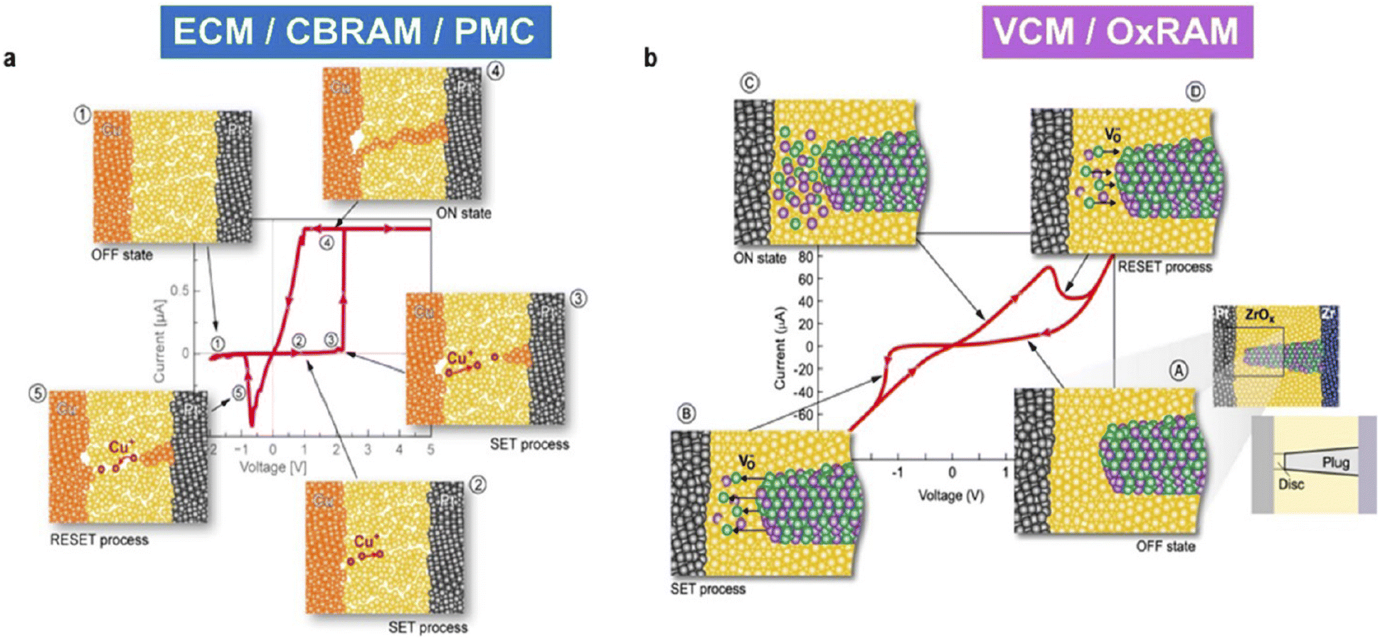 | ||
| Fig. 2 Switching in various RRAM types (a) electrochemical metallization memory and (b) valence change memory.44 | ||
In the literature, multiple surveys focusing on the RRAM have been presented previously. However, there is no survey which primarily focuses on the application-centric nature of RRAM. Therefore, our survey draft is important, as it focuses on a wide domain of applications where RRAM can be used. The remainder of the paper is divided into the following sections: first we will discuss the important concepts of hyperdimensional computing and use of RRAM to realize such architectures in Section II. Section III and Section IV discuss the applications of RRAM in the cryogenic memory and reservoir computing applications, respectively. More information about the architecture utilising RRAM for hardware security applications is detailed in Section V. The concepts of in-memory computing, neuromorphic computing and probabilistic computing approaches utilising RRAM are elaborated in Sections in VI, VII, and VIII, respectively. The memristive sensor approach is discussed in Section IX. The use of RRAM for various applications such as electronic skin, radio frequency (RF) switches and ternary logic is presented in Sections X, XI, and XII, respectively. Finally, the summary and the outlook in Section XIII conclude the paper.
II. Hyperdimensional computing
The development of novel machine learning (ML) models, creative algorithms that use these models, cutting-edge hardware architectures that can support these procedures, as well as cutting-edge tools for energy-saving executions of said designs are all examples of how quickly the area of ML is progressing. In this regard, hyperdimensional (HD) computing serves as an example. A computer paradigm based on the brain that uses various tasks on multidimensional binary-vectors is called HD computing.109 In contrast to deep neural networks, it does not require extensive hyperparameter tuning.110 Rapid and energy-efficient training and inference are possible with HD computing.111 This study focuses on effective HD computing hardware implementations using cutting-edge nanotechnologies. Similar to other machine learning computing models, HD computing hardware implementations are anticipated to (1) securely incorporate computation as well as storing data to minimize the energy usage and delay connected with data transmission;112 (2) utilize streamlined circuit designs (possibly involving approximation) to conserve energy as well as accomplish satisfactory precision stages as dictated,113 and (3) harness the inconsistency inherent in fundamental tools (unlike relying solely on a single technology to perform a given task) like the HD which utilises randomness or instabilities.114Monolithic integration in three dimensions is frequently used to achieve closely integrated energy-efficient memory and compute units. This method uses short, high-density interlayer vias, similar to the usual vias employed in connecting layers of the metal found in joints of modern Integrated Circuits (ICs),115,116 to vertically integrate many layers of transistors and memory in a sequential way. When checked with the conventional chip layering,117 uniform incorporation in three dimensions has the potential to provide more memory bandwidth and higher orders of magnitude.118 Through the use of technologies like RRAM and carbon nanotube field-effect transistors (CNTFETs), which can be manufactured at low temperatures (less than 250 °C), monolithic three-dimensional integration has been demonstrably made practicable.33 For example, CNTFETs have the potential to outperform a silicon CMOS in terms of energy-delay-product by about an order of magnitude, enabling computation that uses less energy. RRAM is a developing memory technology that has the potential for significant data storage capacity in a non-volatile manner, including multi-bit storage per cell. When compared to DRAM, this technology provides improvements in terms of its data density, speed and energy efficiency.119
Moreover, a cognitive-based HD computer nano-system was proposed by Tony F. Wu et al.,120 and the system can be used to recognise languages. They created efficient circuit blocks integrating CNTFETs with detailed and precise access to RRAM memory using unified 3D assembly of CNTFETs and the RRAM device. The use of monolithic 3D assembly of CNTFETs and RRAM in computing system topologies has the potential to considerably improve the energy efficiency of many upcoming applications by lowering the energy consumption product and execution time. Some of the mentioned skills have been employed to demonstrate HD-computing processes in addition to the whole method implementations.108,121,122 CNTFETs are considered amongst the emerging transistor technologies that promise a significant enhancement in the power-time trade-off, which is a measure of energy effectiveness in digital devices. CNTFETs use numerous carbon-nanotubes (CNTs) as channels that assume the shape of cylindrical carbon atom arrangements with diameters ranging between 1 and 2 nm. Also, CNTFETs offer improved mobility of the carriers and electrostatic control. Interestingly, CNTs accommodate digital logic components with a low operating power.123,124 CNTFETs are affected by peculiar variations in CNTs, such as variations in the count of CNTs within a CNTFET, apart from the inherent method disparities found in silicon-transistors, such as disparities associated with the length of the channel, thickness of the oxide material and onset voltage. These variances can cause fluctuations in drive current, which can cause delays in digital circuits. To mitigate these differences, techniques such as optimised process and circuit design can be used.125,126
Nonetheless, as demonstrated by Wu et al.,122 these innate modifications are easily leveraged in HD processing to create seeded hypervectors through fluctuations in the threshold power and CNT number. Inconsistency and uncertainty effectively function as computational resources in this scenario. The hardware implementation of HD computing can be accomplished through unified 3D assembly of CNTFETs and the RRAM device, providing great accuracy in pairwise language categorization.120,122 As illustrated in Fig. 3, the different characteristics of CNTFETs as well as the RRAM device might be employed in building a compact CNTFET-based low power circuit through precise contact with RRAM devices. The diagram illustrates 32-functional pieces networked in parallel, with every piece displaying the HD classifier, HD encoder, and Random Projection Unit (RPU), each utilising specific CNTFET and RRAM features. The RPU, which is reset by clk2, employs CNTFET and RRAM changes in delay devices to conduct random input-to-hypervector mapping. The HD encoder employs CNTFET digital logic for hypervector multiplication and permutation, as well as HD approximation incrementers that take advantage of RRAM's progressive reset feature for hyper vector accumulation. Subsequently, the HD classifier compares the hyper vectors using RRAM and CNTFET Ternary Content Addressable Memory (TCAM) devices via current averaging. When implemented for smaller technology nodes, such as the 28 nm node, this system may accomplish both lower latency and low power consumption, exceeding classic silicon-based CMOS techniques. It, for example, shows a significant improvement with around 7.6 × lower energy consumption with 4.6 × fast execution time.120,122
 | ||
| Fig. 3 Diagram of a monolithic three dimensional HD system utilizing RRAM and CNTFETs.108 | ||
The fundamental differences in CNTFETs and RRAM may be utilised to create an item memory for mapping input letters to hypervectors using randomly generated seeds, as shown in Fig. 4(a–d). Delay cells are employed in transforming the level of the device deviations into delay variations, like drive-current fluctuations caused by changes in CNT count or CNTFET onset voltages, as well as deviations in the RRAM's resistance. Therefore, to construct hypervectors, each potential input (space character plus the 26 alphabet letters) is plotted from a reference clock-edge to a delay, thereby encoding the inputs using the time reference. Therefore, random-delays were introduced to the reference clock-edge and the input signal via delay units to compute each bit of the hypervector. In a situation when the resultant signals coincide (dropping edges sufficiently near to one another to cause SR-latch), this corresponding output is equivalent to ‘1’. Prior to the training of the structure, the RRAM resistance is reset to a HRS and subsequently converted to a LRS for the initiation of delay cells.
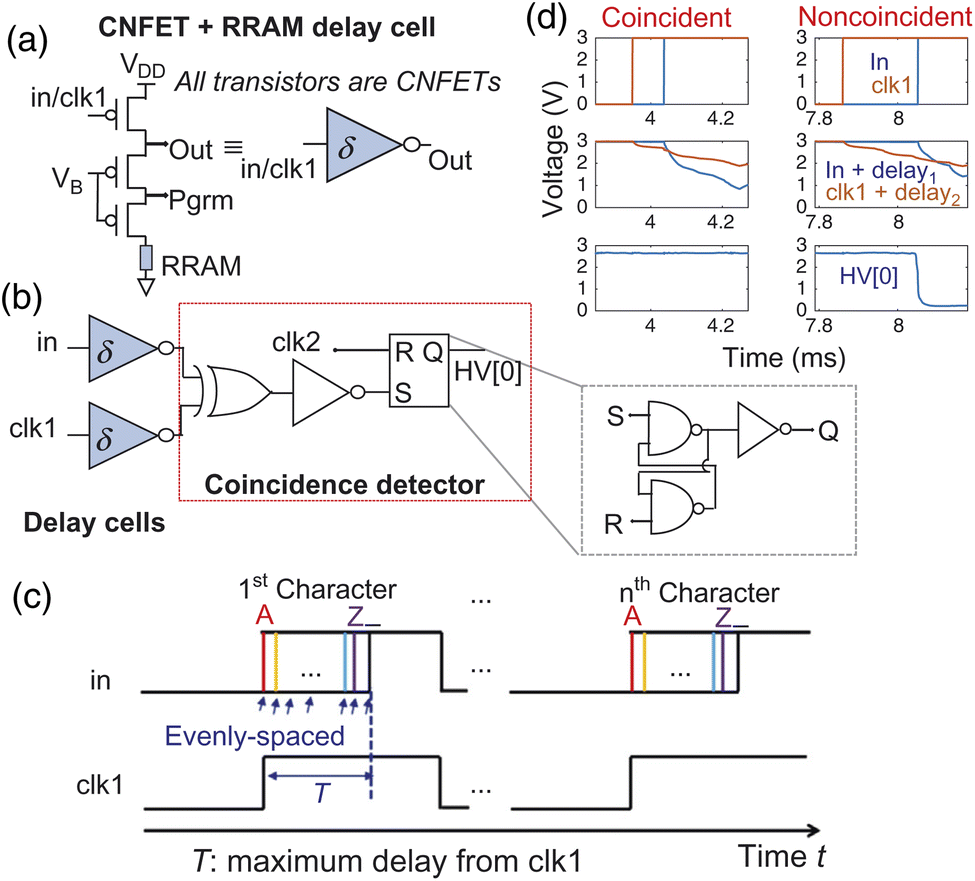 | ||
| Fig. 4 Delay cells that leverage the intrinsic variabilities of RRAM and CNTFETs.108 | ||
III. Cryogenic memory
As transistors continue to scale down in accordance with Moore's law,128 cryogenic electronics is emerging as a technology for enhancing computing efficiency and tackling the problem of static power utilization. The utilization of cryogenic computing is gaining recognition because of its diverse applications, including aerospace electronics and quantum and cloud computing.127,129–132 Operating at cryogenic temperatures offers several advantages for ICs like enhanced reliability, reduced noise levels and increased switching speed, as depicted in Fig. 5. The demand for electrical equipment that can operate in cold temperature (cryogenic) environments is generally regarded as an ideal property for applications in deep space. Nevertheless, the rising need for processors and memory units to operate at extremely low temperatures is now being driven by both quantum and high performance computing, in particular. Quantum computers typically function in the range of millikelvin (mK). However, there is a demand for interface structures functioning at helium-temperatures (4 K) and memory sub-systems able to function at the boiling point of liquid-nitrogen (77 K) to provide more affordable alternatives.133–135 Therefore, this approach could possibly bridge the gap between operating at cryogenic temperatures of helium or lower and room temperature.136 Recent demonstrations have highlighted the advantages of cooling memory systems and processors at cryogenic temperatures as low as 77 K, which corresponds to the boiling point of liquid nitrogen.137,138 The research presented in ref. 139 and 140 primarily centers around conventional embedded memory systems that rely on 6T-SRAM, or six-transistor static RAM. These systems have presented substantial performance enhancements. Nevertheless, the relatively large size of the individual memory cells in 6T-SRAM restricts general memory density arranged in the circuit, and the presence of numerous leakage paths in these memories also contributes to this limitation.141 | ||
| Fig. 5 Numerous electrical benefits of semiconductor devices are realized at cryogenic temperatures, opening up possibilities for practical uses.127 | ||
Non-volatile RS devices, including neuromorphic computing and RRAMs, are considered promising prospects for applications involving the next generation of memory devices that should operate at or higher than the ambient temperature. Nevertheless, it is essential to comprehend their ability to operate under cryogenic conditions before considering them as fundamental components for large scale quantum technologies through the integration of classical quantum electronics. To establish the feasibility of resistive memories operating under cryogenic conditions, it is imperative to demonstrate unipolar and bipolar non-volatile RS and a capability of multilevel operation. Additionally, gaining a deeper understanding of how the geometry of the conductive filament evolves during the switching process is essential. Hao et al.142 introduced an intricately designed 2-layer resistive memory device. This device incorporates a RS layer and a thermal enhancement capping layer, which serve to limit Joule heat generation, thereby enhancing the switching performance. Furthermore, the capping layer also functions as a reservoir for oxygen vacancies. This innovative design enables the device to exhibit multilevel RS capabilities across a broad temperature range (8 K to 300 K). The results obtained from the endurance test at 8 K temperature demonstrate that the cryogenic resistive memory device is capable of switching >106 cycles. Additionally, switching characteristics and the conduction mechanism of devices using transition metal oxides at ultralow temperature (4 K) have also been investigated.143 However, it is important to note that this temperature range still falls above the required range for quantum systems, which typically operate between 0.02 K and 1.5 K. This limitation restricts the co-integration of these technologies.
At 1.5 K, multilayer switching for Al203/TiO2−x RRAM cells, built through CMOS-attuned materials and methods, was achieved by Beilliard and colleagues,144 with the characteristic progressive multilevel switching behavior of these devices being investigated to exploit their capability for electronics based on cryogenic analogue resistive memories. Due to the metal:insulator conversion found in the Ti4O7 conductive filament induced by Joule heating, this I–V physical characteristic show a phenomenon known as Negative Differential Resistance (NDR). Analysis of carrier transport in every multifaceted switching I–V graph indicates that something happened during the insulating phase. This behavior adheres to the Space Charge Limited Current (SCLC) framework for every level of resistance. Conversely, the trap-assisted and SCLC tunnelling dominate HRS and LRS processes, respectively, in the metallic-domain. Fig. 6(a) illustrates the schematic of the RRAM device. In Fig. 6(b), binary RS processes at both 300 and 1.5 K are illustrated, displaying current in relation to Vmem data. The device's temperature-influenced I–V graphs during the LRS, as presented in Fig. 6(c), enable us to identify the temperature of the cryostat at which Tc is 110 K, for both positive and negative bias (as seen in the inset). Lan and colleagues showcased an improved Zn-doped HfOx RRAM device utilizing an alloying technique relying on atomic layer deposition.145 This HfZnO RRAM device exhibited notable enhancements, including lower switching voltages (over 20%), reduced switching energy (greater than 3), and improved uniformity in voltage and resistance states. Furthermore, the constant voltage pulse scheme demonstrates exceptional linearity and repeatability in adjusting conductance, achieving an impressive 90% accuracy when applied in a layered perceptron network simulation design, aimed at recognizing modified handwritten digits in the National Institute of Standards and Technology database. What's particularly noteworthy is that the HfOx RRAM performed reliably even under cold temperatures (cryogenic) circumstances, as low as 4 K, in a comprehensive study of its conduction process. These findings pave the way for systematically engineering outstanding durability of RRAM used in a well-ordered method, opening up exciting possibilities for a range of innovative applications, including cold temperature (cryogenic) circuitry and computing with memory (in-memory) for space-based research, quantum computation, and other applications.
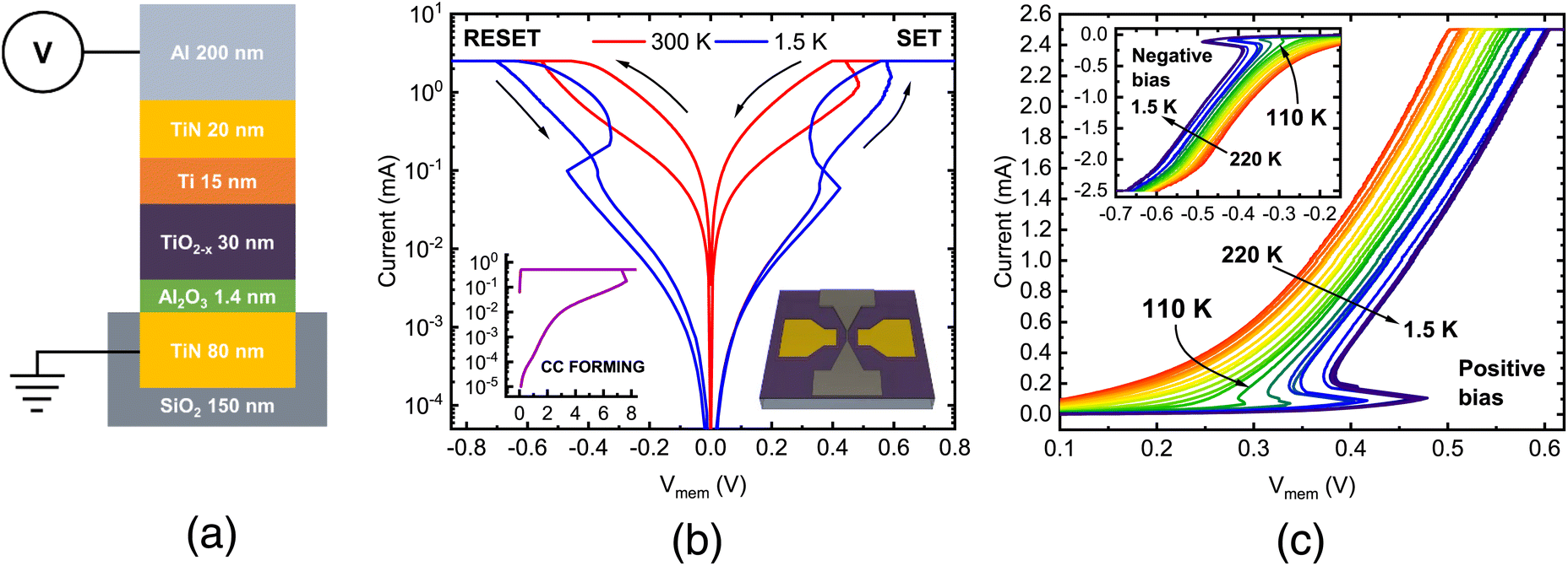 | ||
| Fig. 6 (a) A graphical perspective of an overview of the investigated RRAM cells. (b) A semi-logarithmic graph illustrating RRAM operation phases at two temperatures: 300 K (represented by red-lines) while the blue-lines depict 1.5 K. The forming process is visible in the bottom left inset, having a current-compliance set at Ic = 500 μA. The crosspoint structure is schematically illustrated beneath the rightmost corner. (c) I–V curves in the LRS as a function of temperature, spanning the range from 220 K down to 1.5 K, with a positive bias. The inset provides readings for negative bias. Notably, at a temperature of Tc, the critical cryostat, which is 110 K,144 the NDR influence linked to the metal-insulator transition begins to manifest. | ||
IV. Reservoir computing
Computers have evolved into an essential component of our daily existence. These devices, responsible for performing logical tasks and retaining data, power an array of technologies, including instant messaging, web searches, and intelligent virtual assistants. Given the widespread use of these applications, it comes as no surprise that energy consumption has also surged. Predictions project that by the end of the decade, information and communication technology could account for 8% to 21% of the world's total electricity usage.152 Indeed, specific applications may have a greater impact than others. In an economy heavily reliant on data, advancements in information technology offer advantages across various sectors such as robust computing systems which are indispensable for rapid technological advancement. Nonetheless, if the gap between current computing power requirements and the capabilities of existing technologies remains unaddressed, progress in this regard may be impeded. The substantial increase in data transmission costs linked to the von Neumann architecture, along with the inherent limitations of CMOS technology, pose significant challenges for enhancing energy efficiency.153 Reservoir computing represents a groundbreaking approach for reshaping conventional digital computers and is poised to play a pivotal role in upcoming computing systems.154–156Reservoir computing stands out as a top-tier machine learning technique designed for handling data generated by dynamic systems using sequential data.146,147,157,158 It is worth highlighting that it works effectively with modest training datasets, utilizes linear optimization, and demands minimal computational resources. Reservoir computing, rooted in recurrent neural networks (RNN), presents a challenging concept to be viewed as a more advanced emulation of the human brain, despite its remarkable capacity to process temporal data, as demonstrated in various immediate-term applications.159 Reservoir computing employs a stable and dynamic “reservoir” for iterative data processing and the transformation of data into larger-scale analytical environments. Since the pool's dynamics are steady, only the readout-layer necessitates training, rendering reservoir computing advantageous for cost-effective training, strong adaptability, and rapid learning.148–150
The reservoir computing network, which employs modules for self-feedback, is empirically showcased in procedures exhibiting immediate-term and nonlinear characteristics, and the scenario is illustrated in Fig. 7(A). Features from low dimension feeds are transformed into characteristics in the larger-scale analytical domain by nonlinearity, while immediate-period memory permits networks to refresh their conditions for processing sequential data. But, in practical application, numerous evolving systems featuring immediate-period memory effects and nonlinearity are being employed as storage cells, as illustrated in Fig. 7(B). As an illustration, Ag diffusive devices, which progressively decay with each frame, as depicted in Fig. 7(C), prove to be well-suited for the implementation of the reservoir computing system. In the upper section, the initial presentation of two sequential stimuli triggers the formation of strong conductivity and an uninterrupted Ag filament inside the system, a condition examined in the fourth attempt in the domain. Similar procedures are used to operate the other separate panels, each subjected to different pulse conditions. The resulting conductance varies depending on the dynamic characteristics of the device. This divergence in conductance levels arises from the unique sequences employed. It is important to note that the temporal information is comprehensively captured through the dynamics of ions within the device. In the pursuit to integrate both sensing and computing functionalities, photo-synapses have been engineered using ultra-wide bandgap semiconductor GaO technology, specifically designed for in-sensor fingerprint identification, as is evident from Fig. 7(D). When subjected to optical stimuli, these photo-synapses exhibit a response pattern akin to that observed in Ag electrical diffusive systems, as illustrated in Fig. 7(E). Thanks to the photosensitive reactivity of the elements based on GaO, the reservoir computing structure can function without the need for data communication among the reservoir and the sensor. Besides RRAM devices, experimental implementations of reservoir computing have been achieved by utilising magnetic-skyrmions, and the complex patterns of spintronic generators and nanowires.160–162 Reservoir computing showcases remarkable proficiency in handling temporal and recognition challenges, achieved through the mapping of input data into high-dimensional spaces and states updates at each time frame. For example, the task of recognizing handwritten digits is accomplished by transforming pixels into pulse patterns,163 as illustrated in Fig. 7(F). Conversely, exceptional results are observed in time-series estimation tasks, such as the challenge of the Mackey–Glass sequence,151 as is evident from Fig. 7(G). Some of the benefits of low power usage and compatibility with the system's architecture underscore the immense prospect of employing reservoir computing in the field of sequential estimation.
 | ||
| Fig. 7 (A) A typical reservoir computing system's architecture.146 (B) The fundamental dynamic reaction of a reservoir computing system.147 (C) The electrical synapses can provide history-dependent responses in every framework under distinct programmed sequence signals.148 (D) The photo-synapses can detect optical stimuli and modify conductance in accordance with optical patterns.149 (E) Input processing and output sampling. As the classification foundation, samples 1 and 2 are evaluated.149 (F) Recognition of handwritten digits via the RC device based on a memristor system. As node inputs, the pixels are stored as spike patterns with varying frequencies.150 (G) Automated modelling of Mackey–Glass data sets using a reservoir computing system based on RRAM.151 | ||
Over the year, RRAM has garnered significant attention in the context of reservoir computing due to its suitability as a physical resistor. In a study published in 2021, a Ti/TiO2/Si cell having varying dopant concentrations on a silicon surface was fabricated and characterized.164 They utilised the Ti/TiO2/p+Si cell's short-term effect to construct the storage computing architecture, allowing for the differentiation of 4 bits (16 states) through the application of various pulse sequences to the cell, which works well when used for pattern identification. It has been convincingly shown that RRAM devices exhibiting short-term memory effects are capable of acting as reservoirs within reservoir computing systems. Fig. 8 illustrates a schematic representation that includes a readout, through a pulse stream to a pulse input mechanism. At the outset, it calculates the weights through straightforward learning algorithms during training. Hence, the reservoir system offers cost-efficiency benefits in training. In order to depict the input signals within the storage level using RRAM devices, it employed encoding with four bits through short-term effects. The task of recognizing input images involves distinguishing the digits inside every picture and forwarding them to the storage via short-period effects. To convey the binary data for every pixel in the image, they are converted into pulses, serving as the storage's input signal. The storage is then connected to these pulse stream points of data and subsequently plotted into the larger-scale analytical domain. This approach allows for the differentiation of pixel images with 4 bits per row. Images with a higher pixel density in a single row can be accommodated by encoding them with 4 or more bits continuously. Kim et al.165 conducted an investigation into the short-term memory features of a glass-based Ni/WOx/ITO RRAM cell for reservoir computing systems. Reservoirs can be physically realized utilising a range of tangible systems and resources. Given that the Ni/WOx/ITO RRAM cell demonstrates non-linearity as well as short-term memory features, it stands out as an appropriate candidate for a tangible storage cell. Verification of the 4-bit arrangements is achieved by the use of different pulse-train sources. Once all 16 states were implemented using four bits, it has been demonstrated that the system can effectively accommodate 5 sets of 4-binary pixel images. This finding implies that with further expansion, the system can handle images comprising 28 × 28 pixels.
 | ||
| Fig. 8 Depiction of the reservoir system comprising 3 notable components (from the left): the output-node, the memristor device and the pulse stream.164 | ||
V. Hardware security
In today's world, the significance of hardware security has surged, surpassing the protective measures applied to software and protocols.166 This heightened concern is notably accentuated by the rapid proliferation of the IoT and cloud-based and edge computing, which has enhanced convenience in our daily lives, but has also resulted in a simultaneous increase in threats to information security.167 Contemporary information security heavily depends on cryptographic mechanisms to establish a substantial disparity between authorized and unauthorized utilization of intended data. In this context, random numbers assume a pivotal role within security algorithms. Presently, the majority of random numbers are generated by software-based algorithms, often using predefined seeds.168–170 These methods are at risk of being exploited by determined attackers, as they can potentially compromise the initial-seeds or the mathematical-algorithms using advanced intelligent processes or computing-power. To guarantee the generation of random numbers, leveraging hardware primitives that possess inherent unpredictability at the physical level represents a highly encouraging avenue. In recent decades, research in this field has produced a plethora of security building blocks, including the true random number generators (TRNGs), an array of defensive mechanisms, physical unclonable functions (PUFs), and various applications designed to fortify different facets of hardware security.171–174 Nonetheless, a substantial portion of these security strategies is closely tied to the CMOS techniques, which are gradually reaching their limits. Additionally, novel attack models and vulnerabilities continue to surface, and the current CMOS technology, on which these security primitives and countermeasures have been developed, is insufficient to effectively counter these emerging threats.In the realm of recent technological advancements, nanoscale technologies like CNTs, memristors, phase-change memory (PCM), and two-dimensional (2D) materials have come to the forefront, offering notable improvements in terms of performance and speed when compared to traditional CMOS methods.175 However, these emerging technologies are still in the early stages of development, and they possess some distinctive characteristics that may somewhat restrict their comprehensive integration into memory applications and standard logic processes. Although much of the research has concentrated on optimizing their energy efficiency, reliability and performance, there remains a significant gap in exploring their potential applications for enhancing security measures.
On the other hand, PUFs are gaining prominence as exceptionally reliable hardware security primitives for purposes such as device key generation and authentication.177 PUFs typically harness the inherent variations in the manufacturing process and the physical randomness of the device, rendering them highly dependable and resistant to cloning.178 PUFs operate on the concept that a device-specific, unique key can be generated on-the-fly rather than storing a predetermined set of keys. The fundamental principle of a PUF involves computing a distinct output response in response to an applied input challenge, thus establishing a challenge–response pair (CRP). This CRP is of utmost importance in the development of security protocols, encompassing tasks from device authentication to the encryption of data. This method significantly enhances security by thwarting potential adversaries from gaining access to stored keys and simultaneously reduces the cost associated with creating secure storage slots. A PUF is frequently described using a black-box model, where the challenge vector, originating from the input space, is translated into the response vector within the output slot. The mapping function in this context remains entirely concealed, unidirectional, and exclusive to the specific device. This function is intimately linked with the device's intrinsic characteristics, and manufacturing variations can further induce this distinctive behaviour. The practical utility of PUFs hinges on the quantity of available CRPs obtained. PUFs can be categorized into two types based on the size of their CRPs as stated: a (a) strong PUF and (b) weak PUF. A strong PUF offers a significantly larger CRP space, which ideally grows exponentially with the size of challenge bits. In contrast, weak PUFs typically support a limited number of CRPs, which could be loosely described as linearly dependent on the number of components subject to intrinsic variation.179,180 Consequently, securing and restricting access to weak PUFs becomes crucial, a consideration that doesn't apply to strong PUFs. In most scenarios, weak PUFs are used as a substitute for storing keys in non-volatile memory to deter key extraction, and the derived key can be used for for device identification and certain cryptographic applications, while in the case of strong PUFs, owing to their more extensive CRP space, they offer greater versatility and are well-suited for secure authentication purposes.
Interestingly, a RRAM-based PUF has garnered considerable interest among the recent PUF based devices. It has the capacity for high-density integration and a reduced BER. The inherent variability found in RRAM technology serves as a valuable entropy source for crafting PUF designs. In particular, the variations in the HRS of RRAM devices are frequently employed as the source of entropy for integration due to their broader distribution range in comparison to the LRS. An illustrative RRAM-based PUF configuration is presented in Fig. 9. Initially, the crossbar is provided with an entropy source derived from a prior TRNG system. Subsequently, the PUF's responses are gathered by applying electrical challenges to the rows of the crossbar.176 These challenges are translated into a read voltage pulse before being applied to the crossbar. Leveraging the inherent device variations and the input challenge, Kirchhoff's current law is employed to aggregate the current flowing through each device along the lines of the column. Furthermore, the sneak-path current within the crossbar adds to the current in each column, and this contribution is inherently random. At the output, a current sense amplifier (CSA) is employed to transform the analog current values into boolean response bits. Additionally, a multitude of CRPs are collected to evaluate various PUF properties. An early RRAM-based PUF, as described in ref. 182, has been designed and produced using a weak-write method for producing behaviour within cells that is influenced by procedure variations. Moreover, an enhanced robust PUF embedded is showcased in ref. 183, demonstrating flexibility without requiring further design work modifications. The PUF introduced in ref. 184 takes advantage of write time variation and sneak path-current to get the most the distinctive settings for various response bits. However, in ref. 185 a Voltage Sense Amplifier (VSA) is employed to create a robust intermediary PUF using a 1T-1R bit cell configuration. Additionally, other variations of RRAM-based PUFs with reconfigurability have been suggested. The reconfigurable approach entirely replaces the current CRP storage of the PUF. Lin and his colleagues showcased a reconfigurable PUF, achieving an impressively low inherent BER of approximately 6 × 10⁻⁶ for a response bit length of 128 bits.186 Reconfigurability is achieved by capitalizing on the cycle-to-cycle fluctuations in device resistance. To clear the CRP space, all devices are initially set to the LRS. Subsequently, a RESET pulse is applied, leading to the stochastic redistribution of device resistances across the entire array. The response bit can then be generated using the resistance evaluation method.
 | ||
| Fig. 9 PUF based on RRAM that demonstrates challenge response generation showing the sneak path current as indicated in red color.176 | ||
Random number generators (RNGs) play a vital role in various applications, including problem-solving methods, industrial simulations, computer gaming, and hardware encryption modules used in communication systems.187 Certain crucial applications, particularly in the realm of security where key generation is crucial, demand random number sequences that must meet stringent statistical testing criteria.188 There is a demand in these applications for devices that can fulfill these requirements by extracting entropy from physical phenomena like metastability, jitter, and more. RNGs that derive randomness from physical sources are referred to as TRNGs.189 In recent times, TRNGs have become essential considering the increasing security concerns in the IoT era. As a result, various TRNGs have been previously showcased using sources such as thermal-noise,190 random-telegraph-noise (RTN),191 and current-fluctuations.192 However, these TRNGs possess limitations related to operating power, scalability, and susceptibility to external factors like temperature. They often require post-processing methods to meet the stringent testing requirements. Therefore, RRAM devices have emerged as a promising technology due to their advantageous characteristics. RRAMs are compatible with CMOS technology and they also have fast switching-speed, low power of operation, durability, and scalability. Moreover, Yang et al. presented a TiN/Ti/HfOx/TiN RRAM-based TRNG that leveraged the merging of the HRS and the time delay in the reset process.181 The schematic depicted in Fig. 10(a) illustrates the circuit components. These components encompass the RRAM core within the array, along with an additional capacitor. Additionally, peripheral circuitry elements such as a 1-bit counter, a comparator, resistor, clock sampling, and a switch are incorporated. As a result, it occupies a smaller chip area and consumes less energy. The essential laboratory-established circuit is also depicted. The associated TRNG process and signal diagram are outlined in Fig. 10(b) and (c) respectively. Upon activation, a reset pulse is used in charging the RRAM core. To assess the randomness of the complete reset process, during the TRNG circuit simulation various constant resistors are initially used in place of the RRAM. The measurement curve of RRAM charging and discharging is notably distinct from the simulation results using constant resistors, as depicted in Fig. 10(d). Furthermore, SPICE simulations of the TRNG circuit utilizing the variability aware RRAM model are conducted to confirm the enhancement of entropy. However, in Fig. 10(e), through TRNG circuit simulations, one million bit sequences are produced in order to evaluate the effectiveness of the cross-correlation and auto-correlation constants. Moreover, the auto-correlation constants for different sequence lengths are below 0.003 throughout a 95% confidence-interval, while the cross-correlation constants among 1M bit-streams are all below 0.2. This indicates that the TRNG exhibits high independence and meets the desired criteria, as presented in Fig. 10(f).
 | ||
| Fig. 10 (a) The planned TRNG circuit based on RRAM reset. (b) The TRNG circuit procedure generating true-random bits. (c) Illustration of the plan for the generation of true-random bit-streams. (d) The measurement of the RRAM voltage taken at the electrode. Readings and experimental predictions are shown by dotted and solid lines, respectively. (e) This shows that between the ten 1M bit sequences produced by the TRNG, the pair-wise correlation coefficients are less than 0.2. (f) The parameters of autocorrelation of 1M bit-streams produced by the TRNG are below 0.003 within a 95% confidence-interval.181 | ||
VI. In-memory computing
ML, particularly within the domain of deep learning (DL), has played a pivotal role in pushing recent fundamental advancements in AI techniques.195 DL relies on computational models inspired to some extent by biology, employing networks of interconnected simple computing units that operate in parallel. The success of DL is contingent upon three crucial factors: (a) the availability of expansive datasets, (b) the continuous growth in computing power, and (c) ongoing algorithmic innovations. While DL solutions have led to substantial improvements across various AI tasks, there has been an exponential surge in the demand for computing power.195 Recent analyses reveal a 300![[thin space (1/6-em)]](https://www.rsc.org/images/entities/char_2009.gif) 000-fold increase in this demand since 2012, with projections suggesting a doubling every 3–4 months—an acceleration surpassing historical improvements under Moore's scaling, which exhibited a seven-fold enhancement over a comparable time frame. Simultaneously, the deceleration of Moore's law in recent years, combined with indications that scaling down CMOS transistors may encounter limitations, underscores the necessity to explore alternative technology roadmaps for creating scalable and efficient AI solutions.195,196 It is crucial to recognize that transistor scaling is not an exclusive avenue for enhancing computing performance. Architectural innovations, including graphics processing units (GPUs), field-programmable gate arrays (FPGAs), and application-specific integrated circuits (ASICs), have significantly contributed to the advancement of machine learning.113 A notable trend in modern computing architectures for ML involves a departure from the traditional von Neumann architecture, which physically separates memory and computing. In this context, in-memory computing (IMC) has emerged as a novel paradigm, providing potential solutions to address or alleviate the memory bottleneck—an essential consideration for energy efficiency and latency in contemporary digital computing.113
000-fold increase in this demand since 2012, with projections suggesting a doubling every 3–4 months—an acceleration surpassing historical improvements under Moore's scaling, which exhibited a seven-fold enhancement over a comparable time frame. Simultaneously, the deceleration of Moore's law in recent years, combined with indications that scaling down CMOS transistors may encounter limitations, underscores the necessity to explore alternative technology roadmaps for creating scalable and efficient AI solutions.195,196 It is crucial to recognize that transistor scaling is not an exclusive avenue for enhancing computing performance. Architectural innovations, including graphics processing units (GPUs), field-programmable gate arrays (FPGAs), and application-specific integrated circuits (ASICs), have significantly contributed to the advancement of machine learning.113 A notable trend in modern computing architectures for ML involves a departure from the traditional von Neumann architecture, which physically separates memory and computing. In this context, in-memory computing (IMC) has emerged as a novel paradigm, providing potential solutions to address or alleviate the memory bottleneck—an essential consideration for energy efficiency and latency in contemporary digital computing.113
Various IMC concepts have been proposed that differ in the degree of integration between memory and computation, as illustrated in Fig. 11. The conventional von Neumann architecture (Fig. 11(a)) features physically separate memory and computing units. This leads to significant latency and increased energy consumption due to the movement of input and output instructions.193,197,198 To address these issues, one solution is the concept of near-memory computing (NMC), depicted in Fig. 11(b). To mitigate latency, embedded nonvolatile memory (eNVM) is incorporated on the same chip as the computing unit.99,112 In NMC, eNVM functions as dedicated data storage for parameters and instructions, while SRAM acts as a cache memory for intermediate input/output data.
 | ||
| Fig. 11 Depiction of diverse computing architectures: (a) illustration of the von Neumann architecture, featuring a separated central processing unit and memory unit, interconnected via a data bus. (b) Near-memory computing architecture integrates a processing unit with an eNVM unit for storing commands and parameters. (c) SRAM-based in-memory computing involves direct computation within the SRAM unit using dedicated peripherals, while eNVM acts as storage for computational parameters. (d) eNVM-based in-memory computing utilizes eNVM for both nonvolatile storage and computation. (e) Schematic representation of the memory hierarchy in conventional CMOS-based computing systems, showcasing the trade-off between access speed and capacity. Registers and cache memories near the CPU offer fast access with limited capacity, while memories farther from the CPU exhibit slower access with larger capacity. Notably, storage class memory serves as a bridge between high-performance working memory and cost-effective storage devices.193 | ||
A more integrated solution is represented by IMC as shown in Fig. 11(c). In this approach SRAM functions directly as a computational engine, particularly in accelerating tasks such as matrix-vector multiplication (MVM).199 An inherent drawback in this technique is the need to transfer computational parameters from local eNVM (or off-chip DRAM) to volatile SRAM every time computation occurs. To address this challenge, the ultimate approach for maximizing memory and processing integration is IMC within the eNVM, as depicted in Fig. 11(d).200 Emerging memories, capitalizing on their scaling advantages, 3D integration capabilities, and nonvolatile storage of computational parameters, exhibit promise as eNVM in integrated IMC architectures. Achieving synergy across device technologies, circuit engineering, and algorithms necessitates a comprehensive co-design effort spanning multiple disciplines.
The memory hierarchy of CMOS-based computer systems is portrayed in Fig. 11(e). These systems feature on-chip registers and SRAM at the top, followed by off-chip DRAM and nonvolatile flash storage. Access time reduces from top to bottom, while area density and cost decrease from bottom to top. Notably, owing to 3D integration, NAND flash achieves the highest density.201 Emerging memories, on the other hand, aim to strike a more favorable balance between performance, space, and cost in this configuration. These devices employ innovative storage methods rooted in the physics of materials, offering advantages in scalability, integration within 3D structures, and energy efficiency.
There are several fundamental physical characteristics that enable RS devices to be used for IMC architectures. The ability to store and seamlessly switch between two non-volatile states of resistance/conductance values (binary storage capability) is critical for computing applications.205,206 This non-volatile binary and analog storing capability is useful for IMC primitives, particularly MVM. Physical laws such as Ohm's law and Kirchhoff's current summation laws are used in this procedure. Cai et al. demonstrated a System on Chip (SoC) that incorporated RRAM tiles, analog peripheral circuitry, and a RISC-V processor on a single die.194 The RRAM tile, which is designed as a programmable intellectual property (IP) block, is a key component in the construction of various neural networks. Fig. 12(a) depicts a VMM operation computed in analog in-memory using a parallel read method. Digital-to-analog converters (DACs) transform neural weights, which are represented by various conductance levels, into voltage, which is subsequently given to the memory array. Using analog-to-digital converters (ADCs), the current in each column is measured in parallel and decoded to obtain dot-product results. A 65 nm technology node SoC chip is manufactured utilizing a split-fab technique, in which the foundry deposits CMOS circuits and back-end-of-line (BEOL) metal layers up to the RRAM bottom metal layer. The wafer is subsequently sent to the Applied Materials META R&D foundry, along with the other metal layers, for RRAM integration. RRAM devices are built using a 1T1R architecture, with filamentary RRAM (f-RRAM) sandwiched between two metal layers in the BEOL (Fig. 12(b)). While f-RRAM normally requires an extra high voltage for the one-time formation phase, it benefits from a bigger memory window.119 During the forming and programming phases, the series transistor ensures exact current compliance and controls filament geometry and stochastic behavior. Fig. 12(c) depicts a typical DC I–V curve for the f-RRAM, exhibiting bipolar switching with discrete set and reset operations. The chips are sliced and packaged in a pin-grid-array (PGA) for silicon testing after RRAM integration and metal deposition on the top layers. A custom PCB is constructed employing a FPGA for digital control signals and data transfer for simplicity of testing, as shown in Fig. 12(d).194
 | ||
| Fig. 12 (a) In-memory computing utilizing analog techniques with a memory array. The VMM is executed through a parallel read operation, where input bits undergo conversion to a pulse train via bit-serial DACs, facilitating bit-wise multiply-accumulate (MAC) computations. (b) Depiction of RRAM integrated into the 65 nm BEOL process. The inset shows a transmission electron microscopy image of the RRAM stack showcasing contacts to both top and bottom electrodes. (c) I–V curves illustrating the behavior of Fe-RRAM devices. Arrows indicate the sweep direction for set and reset operations. Currents are normalized to arbitrary units, and the forming process is not depicted. Inset: schematic representation of the 1 T1R bitcell. (d) The specially designed PCB tailored for silicon testing and the demonstration of AI applications.194 | ||
VII. Neuromorphic computing
A significant challenge in neuromorphic engineering lies in the development of innovative devices that mimic the functions of biological elements within a neural network, such as spiking neurons and learning synapses.202–204,207–211 In this context, resistive (or memristive) devices, particularly RRAM, have attracted considerable interest due to their simple structure, low-power operation, and seamless integration with the CMOS process flow.212–214 The ability to control device conductance through electrical stimuli, similar to neuronal spikes inducing potentiation and depression in biological synapses, has driven the development of artificial synapses utilizing RRAM devices.215–217 The research in the neuromorphic computing domain has diverged into two primary directions: (i) the development of Artificial Neural Networks (ANNs) aimed at highly accurate recognition of image, video, and audio data,218 and (ii) the engineering of Spiking Neural Networks (SNNs) to closely emulate the adaptability and high-energy efficiency observed in the human brain.219 The scaling behavior of RRAM devices, in terms of both device area220 and 3D integration,221 facilitates the implementation of high density of synapses essential for both DL architectures and brain-inspired circuits, fostering robust connectivity between neurons and synapses. Similar to how biological synapses influence communication among neurons, the resistance states of nonvolatile RRAMs can modulate the connections among artificial neurons.222,223A biological neuron receives spike signals from presynaptic neurons and integrates them into its membrane potential, as illustrated in Fig. 13(a).202 The membrane potential of the neuron increases when spikes occur within a specific interval. Upon reaching the threshold potential, the neuron generates spikes directed towards its post-synaptic neuron. However, due to the leaky integrate behavior, if the presynaptic neuron ceases to send spikes and the membrane potential drops below the threshold, the potential returns to its initial level, known as the resting potential. The leaky-integrate-and-fire (LIF) neuron model provides a detailed description of these features observed in biological neurons.224
 | ||
| Fig. 13 (a) A visual representation comparing a biological neuron to its artificial counterpart utilizing memristor technology.202 (b) Diagram illustrating a 3-terminal memristive synapse within a Spiking Neural Network (SNN) implementing supervised learning.203 (c) Schematic representation of memristor technology based synapses. (d) Illustration of an SNN trained for a classification application using Spike-Timing-Dependent Plasticity (STDP) rules. The network's accuracy shows improvement proportional to the number of memristive synapses.204 | ||
In SNNs, the hardware design for supervised learning (SL) favours 3-terminal memristive synapses, with the third terminal providing supervisory signals. Chen et al.203 demonstrated 3-terminal memristive synapses for SL in SNNs, as schematically represented in Fig. 13(b). When applied to an SL problem, the complementary synapse and neuron circuit are built to perform the remote supervised method (ReSuMe) of a SNN, exhibiting rapid convergence to effective learning through network-level simulation. Boybat et al.204 proposed the concept of a multi-memristive synapse, which is schematically depicted in Fig. 13(c).
The collective conductance of N devices determines the synaptic weight in this synapse. Utilizing numerous devices to represent a synaptic weight enhances the overall dynamic range and resolution of the synapse. To achieve synaptic efficacy, an input voltage comparable to neural activation is applied to all constituent devices. The net synaptic output is the sum of individual device currents. Researchers explored the impact of multi-memristive synapses on the training of both ANNs and SNNs. They developed a spiking neural network using a Spike-Timing-Dependent Plasticity (STDP)-based learning technique for handwritten digit recognition. Simulations utilized a multi-memristive synapse model to describe synaptic weights, with devices arranged in either a differential or non-differential architecture. The increase in the number of devices per synapse resulted in a corresponding improvement in the network's categorization accuracy. The simulations were conducted with five different weight initializations, and the test accuracy was obtained from a double-precision floating-point implementation as represented by the dotted line.
Numerous research reports highlight the maturity of RRAM devices crafted from inorganic materials like oxides, solid electrolytes, and 2D materials, showcasing robust performance. This provides a promising avenue for exploring the application of organic materials, including biological and polymer materials, in RRAM devices. The performance of these devices is intricately linked to RS mechanisms, with a significant reliance on the selection and processing techniques applied to thin film materials. To effectively integrate RRAM devices as synapses in neuromorphic systems, a comprehensive comprehension of the meta-plasticity mechanism and internal states of these memristive devices is indispensable. The elucidation of the underlying mechanisms governing RRAM devices is inevitable and will stem from investigations into conduction and RS mechanisms, drawing insights from both experimental results and simulations. Further advancements in research should encompass the interplay between materials, device levels, circuit designs, and computing processes, promising to accelerate the realization of RRAM synapses for neuromorphic computing systems.
VIII. Probabilistic computing
The von Neumann architecture poses limitations in conventional computing systems, requiring significant computational and memory resources, leading to prolonged operation times for solving classical problems like combinatorial optimization and invertible logic. To effectively address these challenges, researchers have been continuously exploring innovative computational methodologies. Probabilistic computing, emerging as a revolutionary paradigm, offers a promising approach to tackle these difficulties efficiently and with minimal power consumption, referred to as a p-circuit.225,226 At the core of the p-circuit lies the probabilistic bit (p-bit), a resilient unit that fluctuates between 0 and 1 over time, in contrast to typical binary digital circuits where bits rigidly represent either ‘0′ or ‘1’.227 p-bits interact with one another within the same system using specific principles.Employing a p-circuit for implementing Boolean functions provides high accuracy comparable to that of traditional digital circuits and leads to a unique feature—invertibility, which is absent in traditional digital circuits. In the direct mode, the input is clamped, and the network produces an exact output. Conversely, in the inverted mode, the output is clamped, and the system oscillates through all conceivable inputs consistent with that particular output. Meanwhile, in the floating mode, the network dynamically fluctuates among all viable input/output combinations. In a binary stochastic neuron within a neural network or neuromorphic computing system, the p-bit has the probability of being ‘0’ or ‘1’, and the variation in input can modify these probabilities.228,229
In a recent implementation of p-bits, a magnetic tunnel junction (MTJ) served as a stochastic element, as discussed in a study by Borders et al.230 Despite the presence of thermal noise, the magnetization direction changed by lowering the energy barrier that controls the resistance states of the MTJ. A three-terminal p-bit was developed by connecting this stochastic MTJ to an n-type metal-oxide-semiconductor (NMOS) transistor. However, adhering to the p-bit principle, there is no inherent requirement for the MTJ to be the sole p-bit generator; any stochastic electronic device that can be regulated by an external input voltage can be employed. Table 1 provides a comparison of various computing methods.
| Computation methods | Classical computing | Quantum computing | Probabilistic computing |
|---|---|---|---|
| Data expression | Deterministic values 0 or 1 | Superposition of 0 and 1 | Probabilistic values 0 or 1 |
| Infinite states b/w 0 and 1 | |||
| Hardware implementation | Digital logic circuits based on CMOS | Electron spin resonance based computing | Oscillating ouputs of a digital nature |
| Output | Deterministic | Probabilistic | Probabilistic |
| Power consumption | High | High | Low |
RRAM is considered a strong and promising choice for the future development of memory technology while the non-uniformity issue poses a significant hurdle that must be addressed before commercialization.232,233 This non-uniformity stems from the random nature of the switching mechanism in RRAMs. Intriguingly, the same stochastic processes that contribute to the non-uniformity in RRAM have been harnessed for hardware security applications, as mentioned earlier. Additionally, the stochastic characteristics of RRAM hold potential for applications in computing paradigms, including stochastic neural networks.234,235 There are various studies in the literature which introduce a novel application of RRAM's stochastic nature, specifically as p-bits in probabilistic-computing. Liu et al.231 presented an RRAM-based TRNG, and combining this TRNG with an activation function implemented by a piecewise linear function yields a standard p-bit cell, a fundamental component of a p-circuit. To optimize resource utilization and reduce the number of p-bits, a p-bit multiplexing approach is employed. Fig. 14(a) illustrates the overall architecture of the proposed probabilistic computing system, encompassing the p-circuit, UART (Universal Asynchronous Receiver/Transmitter) interface, PC, and controller. The p-circuit integrates the p-bit and weight-logic, crucial for invertible logic. Guided by the weight-logic calculation, the p-bit adjusts the probability of output 1 and awaits sampling by the weight logic. To improve the efficiency, a multiplexing method is utilized, facilitating the serial update of p-bits through a finite state machine (FSM) in the weight-matrix. As illustrated in Fig. 14(b), an N-bit ripple carry adder (RCA) is examined, incorporating two multiplexing techniques. The first technique is applied to the basic unit full adder (FA) of the RCA (Fig. 14(c and d)), resulting in both natural serial updates and a substantial reduction in the number of p-bits. The N-bit RCA is multiplexed using the second multiplexing approach (Fig. 14(b)), with the update order transitioning from FA1 to FAn. Although multiplexing extends the operation time, it proves acceptable for statistical-based probabilistic computing, effectively reducing hardware consumption.
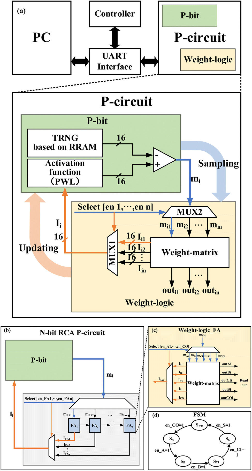 | ||
| Fig. 14 (a) Top: illustration of a probabilistic computing system consisting of a probabilistic circuit (p-circuit), UART interface, PC, and controller. Bottom: detailed structure of the p-circuit, featuring P-bits (green) and weight-logic components (yellow).231 (b) Structure of an N-bit Ripple Carry Adder (RCA) p-circuit employing a two-multiplexing strategy.231 (c) Structure of a full adder utilizing time-division multiplexing in the p-circuit design.231 (d) Depiction of the calculation process within the weight matrix in the context of the described probabilistic computing system.231 | ||
Kyung et al. developed p-computing, a novel computing paradigm based on the threshold switching (TS) behaviour of a Cu0.1Te0.9/HfO2/Pt (CTHP) diffusive memristor.236 p-bits, which are required for p-computing, are realised by the stochastic TS behaviour of CTHP diffusive memristors and interconnected to form a p-computing network. A diffusive memristor, unlike electrochemical metallization cells, is a two-terminal ionic device with volatile TS behaviour, switching to an ON (TS-on) state at a particular threshold voltage and reverting to an OFF (TS-off) state when the voltage is removed. This is in contrast to the behaviour of electrochemical metallization cells, in which the metallic conductive filament remains intact for an extended period of time, guaranteeing persistent memory function. In prior research on memristors as synaptic devices in hardware neural networks or neuromorphic circuits, Boolean logic operations were frequently overlooked. In contrast, p-computing places a strong emphasis on Boolean logic operations, aligning more closely with in-memory logic operations. To effectively implement all 16 Boolean logic operations, the researchers employed a p-computing system based on CTHP memristor-based p-bits. The p-computing network demonstrates the ability to perform logic operations, and the determination of the cost and input functions for all 16 Boolean logic operations was simplified compared to that in earlier studies. The memristor-based p-computing network showcased the implementation of both forward and reverse directions. Moreover, the study illustrated complex functions, including a full adder and multiplication/factorization, demonstrating the methodology's potential for application in more intricate logic circuits. The presented memristor-based p-bits exhibit significant potential for computing hardware based on diffusive memristors, offering a potential solution to the memory wall challenge inherent in existing von Neumann computing approaches.
IX. Memristive sensors
Semiconductor nanowires are currently under investigation for their potential in producing low-cost microchips, positioning them as highly efficient building blocks for miniaturized bioassays utilized in diagnostics and therapies. Notably, silicon nanowire-arrays with memristive electrical capabilities are biofunctionalized with receptor molecules such as antibodies or DNA aptamers, resulting in what is referred to as memristive biosensors.237 These biosensors have proven successful in achieving ultrasensitive detection for cancer biomarkers,238 demonstrating atto-molar concentration sensing capabilities.239 Additionally, they have exhibited effectiveness in screening medicinal compounds and offer the potential for continuous drug monitoring,240 showcasing considerable promise for ultrasensitive and precise biosensing applications. Moreover, the work by Naus et al.241 and Tzouvadaki et al.242 validated the design and implementation of memristive biosensing electrical systems. These technologies facilitate swift, fully automated, and simultaneous sensing outputs from multiple independent memristive biosensors on a single chip. Carrara et al.243 conducted a study emphasizing the growing interest in research on memristors, particularly in the context of various types of memristor sensors encompassing both physical and chemical sensors. The detection mechanism for biomarkers using memristors shares similarities with field effect transistors (FETs), wherein the binding of bioreceptors and biological analytes induces a change in conductance. In memristors, however, the attachment (bio-functionalization) of charged residues on the device's surface leads to a distinct gap in the logarithmic current–voltage curve, as illustrated in Fig. 15.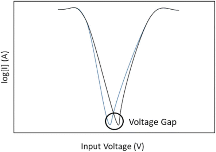 | ||
| Fig. 15 Illustration of the voltage gap in a functionalized memristor biosensor.238 | ||
The primary focus of research on memristive biosensors has been on silicon nanowire sensors. Carrara et al.244 played a pioneering role in this domain by leveraging the memristive effect for biosensing. They covalently functionalized silicon nanowires with rabbit polyclonal antibodies to detect rabbit antigens. Tzouvadaki et al.237 further advanced this field by developing a multi-panel chip capable of biosensing through both electrical (memristor) and fluorescence characterization approaches. This versatile device holds significant potential for point-of-care (POC) applications as it can identify single or multiple biomarkers from a sample containing various target and non-target molecules, utilizing a range of characterization techniques. The device successfully identified rabbit antigens in a sample containing three additional negative control reagents after adjusting the voltage gap.
Several studies have utilized silicon nanowire memristors for the detection of cancer biomarkers, including Vascular Endothelial Growth Factor (VEGF) and Prostate Specific Antigen (PSA). Puppo et al.245 employed nickel silicide to create memristive silicon nanowires with a Schottky barrier at their ends. Their research focused on investigating the impact of humidity variations on covalently functionalized silicon nanowires with anti-VEGF antibodies, successfully detecting the VEGF at concentrations ranging from 0.6 to 2.1 femtomolar. Tzouvadaki et al.239 played a pioneering role in utilizing memristive silicon nanowires functionalized with DNA aptamers for prostate cancer detection. They also verified a prototype memristive biosensing board, which included a sensor module, ADC, MUX, microcontroller, data storage, and power supply. The biosensing component comprised 12 identical memristive nanowires, each generating a unique signal and activated by the same common source. Memristive biosensors based on silicon nanowires have effectively identified non-cancer biomarkers such as Tenofovir and the Ebola virus, in addition to cancer biomarkers. Tzouvadaki et al.240 utilized memristive silicon nanowires manufactured using both top-down and bottom-up fabrication techniques, functionalized with DNA aptamers, to detect Tenofovir in both a buffer and full human serum.
Certain memristors exhibit chemical sensing capabilities, manifesting changes in resistance when exposed to specific compounds.244,246,249–253 Memristive hydrogen gas sensors have been engineered, demonstrating suitability for applications in fuel cells and hydrogen safety.249,250 Additionally, memristive sensors designed for detecting liquid glucose concentrations and proteins associated with tumor tissues and vascular disorders have been developed.245,251–253 Typically, a memristor gas sensor consists of a metal oxide semiconductor serving as the switching and sensing material sandwiched between two electrodes.250 To address process variations and enhance overall performance, Khandewal et al.246 proposed a gas sensor architecture incorporating four memristors (M1, M2, M3, and M4) as shown in Fig. 16(a). In the presence of chemicals, these memristors collectively function as a single sensor, assuming similar gas concentrations. They are designed under identical initial conditions and respond in a manner akin to a target gas. To read the sensed value, a non-zero voltage is applied while ensuring that the sensors remain in a hold state to prevent alterations in their state variables (resistance). The perceived resistance is then obtained by dividing this voltage by the resulting current. This architecture significantly mitigates sensitivity changes due to inherent process variations in chemical sensing applications, while maintaining an overall resistance similar to that of a single sensor. Moreover, the gas sensor design can be reconfigured by incorporating switches (S3 and S4) and an NMOS transistor, enabling the creation of a multifunction logic architecture and a Complimentary Resistive Switch (CRS)254,255 as shown in Fig. 16(b). The impact of memristive magnification was studied for a single device architecture, revealing results similar to those of a single sensor under comparable conditions. The enhanced overall resistance leads to a substantial improvement in read power consumption, as depicted in the lower plot in Fig. 16(c).
 | ||
| Fig. 16 (a) Design and configuration of a 4-memristor gas sensor architecture. (b) The reconfigurable architecture of a 4-memristor gas sensor. (c) Memristive magnification and the consequent read power consumption during the sensing of oxidizing gas.246 | ||
X. Electronic skin
Skin, which is the body's largest organ, plays a crucial role in protecting against external elements, maintaining homeostasis, and facilitating the sense of touch.248,256–258 It harbors an extensive nerve network with diverse sensory receptors distributed across the epidermis, dermis, and hypodermis layers, as illustrated in Fig. 17(a). These receptors detect various internal and external stimuli, including pressure, strain, vibration, temperature, pain, and chemical signals, enabling humans to perceive and interact with their surroundings. This has motivated scientists and engineers to develop electronic skin (e-skin), flexible and stretchable electronic devices or systems that emulate the functions of human skin. Recent advancements in e-skin development focus on materials, structural designs, and functional enhancements, with an emphasis on improving sensing capabilities (stretchability, sensitivity, and long-term monitoring), ensuring user-friendly detection modes (non-invasive, inflammation-free, and implantable), integrating at the system level (data transmission and power supply), and introducing new functions (self-healing).259 However, the perception functionality, essential for mimicking human intelligence, is often lacking in many e-skin systems. The implementation of perception functionality in a flexible and stretchable sensing system, referred to as artificial skin perception, is crucial for achieving genuinely intelligent artificial skin, surpassing the capabilities of human skin, as depicted in Fig. 17(b). When coupled with sensing, feedback, and other technologies, as illustrated in Fig. 17(c), artificial skin perception will significantly advance the development of next-generation soft robotics, requiring low-latency and energy-efficient data processing for fast adaptation to dynamic environments. Presently, the perception processes of most e-skin systems occur in centralized processing units, typically computers or cloud servers located far from the sensing systems generating sensory signals. Transmitting these time-serial, unstructured, and redundant signals to an external processing end results in substantial data movement and energy consumption. Artificial skin perception aims to address these critical issues. | ||
| Fig. 17 (a) Human skin composed of the epidermis, dermis, and hypodermis. (b) Artificial skin comprises sensing, perception, and encapsulation layers. (c) A comparison of the functionalities of human skin and artificial skin. Artificial skin not only replicates human skin functions like sensation, protection, and regulation but also exceeds human skin capabilities with features such as localized perception, super-sensing, and active feedback. (d) Illustration of an artificial reflex arc system integrated with artificial skin perception functionality, as described in ref. 247. (e) Depiction of an artificial nociceptor with artificial skin perception functionality, as presented in ref. 248. | ||
Artificial skin perception has become feasible due to recent progress in materials science, manufacturing processes, electronic device miniaturization, and computing architectures. RRAMs, emerging as nonlinear electronic components, are considered promising for integrating non-volatile memory and advanced computing technology. The memristive mechanism, well-understood and implemented in hardware, has facilitated RRAM's wide applications in next-generation AI, particularly in wearable electronics and artificial e-skin. Flexible memristors in artificial e-skin demonstrate significant potential. Changes in resistance in response to electrical stimulation can serve as a threshold detection criterion. The RS phenomenon in RRAM-based memristive devices is often explained by the formation/rupture of nanoscale conductive filaments, where externally driven ion transport plays a crucial role. This mechanism inherently facilitates the evaluation of information processing thresholds. For instance, He et al. presented a flexible artificial reflex arc system (Fig. 17(d)) comprising a non-volatile RS device for perception, a pressure sensor for tactile sensing, and an electrochemical actuator that functions as a muscle in response to stimuli.247 The RS mechanism is triggered only when the tactile stimulation surpasses a threshold, showcasing threshold computing in the flexible system. This decentralized processing enables a rapid response to pressure stimuli, relieving centralized processing units of time-consuming low-level decision-making activities. In addition to non-volatile RS devices, diffusive memristive devices excel at threshold computing due to their natural threshold effect, wherein created conductive filaments spontaneously break up after the removal of externally applied voltages.99,261 The functioning mechanism of a biological nociceptor and an artificial nociceptor based on memristors is depicted in Fig. 17(e). Nociceptors, located in parts of the human body sensitive to noxious stimuli, generate electrical potentials when detecting stimuli. Electrical pulses from the sensor are applied to the memristor in the artificial nociceptor based on memristors. The memristor switches between ON (LRS) and OFF states (HRS) depending on whether the pulse amplitude reaches the threshold voltage. The detection of an output current at the ON state corresponds to the response to a noxious stimulus.
XI. Radio frequency (RF) switches
Memristive devices with two stable resistive states have applications as radio frequency (RF) switches, essential components for routing or reconfiguring high-frequency signals in wireless communication systems.262–264 In modern wireless systems, a vast number of communication channels spanning a wide range of frequencies, including the terahertz (THz) regime, are employed to transmit multimedia data at high rates, such as 10 Gb s−1 for 5G networks and 100 Gb s−1 for the emerging 6G standard.265,266 While silicon transistors are currently the main technology for RF switches due to advantages in chip integration and cost, they have limitations. Transistors operate in ON and OFF states and are volatile, consuming energy during switching and when idle. This characteristic leads to poor energy efficiency, potentially reducing the battery life of mobile devices.260,267 The energy consumed during switching represents necessary work, but the wasted energy maintaining the ON or OFF states contributes to inefficiency.Oxide-based resistive switches have been extensively studied for memory and neuromorphic computing applications due to their analog switching features. However, their utilization in RF switching has been restricted due to their high ON-resistance states, leading to unacceptable insertion loss. In a theoretical hypothesis presented in ref. 268 a reconfigurable passive planar absorber using RRAM required a LRS of 300 Ω, which was achieved by constructing TiOx-based RRAM devices. However, more advanced RF circuitry demands switches with a significantly lower LRS to minimize insertion loss. Experimental results of an RF oxide RRAM switch for the X-band (Fig. 18(a)), utilizing highly reduced TiOx (30 nm thick) as the active material, were reported in ref. 260.
 | ||
| Fig. 18 Oxide-resistive RF switch. (a) Schematic illustration showing a substoichiometric TiO2−x oxide layer sandwiched between two metal electrodes (Pt). (b) Top view SEM photograph. (c) Characterization results.260 | ||
The device, designed with a coplanar waveguide featuring a 100 μm signal line width and 60 μm gaps to ground to ensure 50 Ω impedance matching, exhibited promising results. The intentional misalignment of the top electrode (TE) from the bottom electrode (BE) was employed to reduce device dimensions below the resolution limit, minimizing capacitance at the cost of some yield. The smallest functional device achieved had an area of approximately ∼0.5 μm2(Fig. 18(b)) Following TE lithography, a 30 nm TiOx layer was deposited in a vacuum through e-beam deposition from TiO2 pellets, followed by electrode metal deposition. This ensured a clean interface between the TiOx layer and TE. The fabricated devices demonstrated highly conductive, nearly linear behavior, with resistances of approximately 38 Ω at 0.05 V. The devices had low switching voltages (1 V) and could be switched at least 20 times at room temperature in an air environment.
Efforts to reduce ON-resistance by using higher set currents led to irreversible damage to the device. At 10 GHz, the switch exhibited favorable insertion loss (−2.1 dB) and isolation (−32 dB) (Fig. 18(c)). The non-volatility of these devices, comparable to that of similar devices reported for other applications,269 and reliable switching for tens of cycles demonstrated superior endurance compared to previously reported RRAM-based RF switches.270 With further device engineering, these devices could potentially achieve greater endurance and improved performance, suggesting the feasibility of oxide RRAM RF switches with endurance surpassing 106 cycles. Advanced nanolithography techniques may further reduce device area for enhanced isolation.
XII. Ternary logic
Arithmetic operations are pivotal in the realm of digital systems, and the conventional design has long been rooted in binary logic, featuring two possible logical values (0 or 1, true or false). In nanoscale design, a critical challenge arises in the form of interconnect limitations, where the lines used for integrated circuit design contribute to noise, delay, and increased power consumption.271,272 Continuous scaling of semiconductor devices has accentuated the importance of interconnects, becoming crucial determinants of integrated circuit performance. To address these challenges, multiple valued logic (MVL) has emerged as a promising solution for modern circuits, offering significant advantages over binary logic in digital system design.273 One key advantage of MVL systems is their ability to transmit more information per wire and store more than one bit of information in each memory cell, a contrast to binary logic systems where each cell can only store one bit of information. This results in reduced interconnect complexity and enhanced storage capacity. MVL circuits employ more than two levels of logic for computation, leading to categorizations such as ternary (base = 3) or quaternary (base = 4) logic systems, depending on the number of logic levels.274 Considering hardware implementation challenges, ternary logic systems with a radix of three have proven to be the most effective implementation of MVL systems.276Various emerging technologies, including CNTFETs, Quantum Dot Cellular Automata (QCA), and Single Electron Transistors (SETs), have been explored for the implementation of MVL circuit designs. Among these, CNTFETs have stood out as a particularly promising technology for design of MVL circuits. CNTs are basically rolled graphene sheets with a cylindrical structure, which are utilized to implement ternary logic gates based on CNTFETs, which share similarities with MOSFET devices used in CMOS logic.277–281 Another suitable technology for realizing ternary logic systems is RRAM primarily due to its ability to handle multiple resistance states without complex additional circuitry which makes it well-suited for configuring logic circuits, including logic gates in digital systems.282 Binary logic gates with nanowire RRAM devices have already been proposed, leveraging RRAM's non-volatility, large on/off ratio, low ON-resistance, and excellent scalability.283 The non-volatility of RRAM devices allows for low power consumption, non-volatile on-chip data storage, high capacity, and simple fabrication, making RRAM highly suitable for MVL circuit designs. A hybrid RRAM/CNTFET architecture for ternary logic gate design has been proposed as an innovative approach. This design utilizes active-load RRAM and CNTFETs, demonstrating significant benefits for ternary NAND, ternary TNOR, and standard ternary inverter (STI) logic gate designs. The proposed approach reduces the transistor count by 50%, offering advantages in chip area, circuit density, and ease of fabrication.284–288 The logic voltage levels considered in this approach are defined as follows: logic ‘1’ is  (0.45 V), logic ‘2’ is Vdd (0.9 V), and logic ‘0’ is 0 V. Utilizing RRAM for implementing ternary logic design opens up new opportunities in the design of digital systems.
In addition to CNTFETs, FinFET technology has garnered recognition for its potential in achieving smaller cell areas with enhanced reliability. FinFETs, owing to their three-dimensional gate coverage over the ultra-thin channel region, offer effective gate control and reduced short-channel effects.289,290 A recent proposal by Yousefi et al. introduces a hybrid RRAM/FinFET-based ternary nonvolatile memory cell along with its array architecture as depicted in Fig. 19(a).275 The schematic layout is depicted in Fig. 19(b). In this architecture, the RRAM device serves as a nonvolatile ternary storage element, while FinFETs are employed to implement the peripheral circuitry. The proposed ternary memory cell adopts a 3-transistor 1-RRAM (3T1R) structure. The writing operation is managed by two p-type FinFETs, whereas the read operation is facilitated by an n-type FinFET. The design incorporates a dual-step ternary write process and a write-isolated read operation, leading to substantial reductions in read and write delays. The ternary RRAM cell operates in three modes: write, read, and hold. The RRAM device serves as the storage element, and FinFETs are responsible for constructing the peripheral circuitry for each operation mode.
 | ||
| Fig. 19 Ternary RRAM cell: (a) circuit schematic and (b) FinFET-based cell layout.275 | ||
The ternary RRAM array architecture is composed of the cell array (CA), which stores the actual data, the pre-charge circuit (PRC) for initializing or pre-charging the necessary signals or lines before specific operations, the row decoder (RD), which selects a specific row of memory cells in response to an address, the column decoder (CD), which selects a specific column of memory cells during a read operation, and the output ternary buffer (OTB) to process and store the output signals from the memory array. Under the control of a Memory Control Unit (MCU), the array operates in three modes: write, read, and idle. The MCU manages the RD, CD, OTB, and DEMUX sections, with the OTB in each line comprising two cascaded STI inverters, serving as a ternary buffer for sensing output node line changes during the read mode as depicted in Fig. 20. The ternary cell structure is also implemented using 7 nm FinFET technology, showcasing the potential of integrating RRAM and FinFET for ternary nonvolatile memory applications.291
 | ||
| Fig. 20 Ternary RRAM array architecture.275 | ||
XIII. Summary and outlook
The investigation of RRAM applications has shown a multitude of opportunities, demonstrating its adaptability and potential influence in many technical fields. Commencing first with the introduction in Section I, which detailed the peculiar RS features of RRAM, the next sections explored particular applications, each providing unique contributions to the technical field. The implementation of RRAM in hyperdimensional computing signifies a fundamental change in computing efficiency. RRAM shows potential in expediting processing activities crucial for AI, machine learning, and data-intensive applications by effectively managing intricate mathematical calculations. The analysis of cryogenic memory applications uncovers the capacity of RRAM to function under highly challenging temperature conditions. The significance of this capacity lies in its relevance to space exploration missions and research activities, where conventional memory technologies may fail. This highlights the durability and adaptability of RRAM. RRAM in reservoir computing presents non-traditional computing techniques. The incorporation of this technology into physical reservoirs for data processing presents a new method for performing computational tasks, demonstrating the potential progress in cognitive computing and analysis of dynamic systems. Furthermore, the random and unpredictable switching properties of RRAM make it a very desirable option for safe data storage and cryptographic applications, effectively addressing weaknesses in current hardware security designs. Moreover, the utilization of RRAM for in-memory computing, as discussed in Section VI, represents a deviation from conventional computer architectures. The incorporation of RRAM into memory-centric processing offers substantial enhancements in speed and efficiency, effectively meeting the increasing need for memory-intensive applications.Section VII highlights the significance of RRAM in neuromorphic computing since it has the ability to imitate human brain-like characteristics. This application facilitates the progress of energy-efficient and flexible computing systems, hence propelling the advancement of the AI domain. RRAM, among other emerging technologies, provides a high level of practicality for simulating biological synapses and neurons. RRAM, as a two-terminal device, has a physical structure that is correlated with biological synapses. By incorporating RRAM into probabilistic computing, as explained in Section VIII, a dynamic component is introduced into computing systems. The intrinsic unpredictability of RRAM is utilized to carry out probabilistic computations, providing benefits in managing uncertainties and improving the resilience of algorithms. Section IX examines the incorporation of RRAM into memristive sensors, demonstrating its capacity in pioneering sensing technologies. RRAM-based sensors demonstrate versatility and precision, hence enhancing the advancement of effective and reactive sensing technologies. The implementation of RRAM in electronic skin, as described in Section X, demonstrates its capacity to generate adaptable and reactive surfaces. RRAM, by emulating the characteristics of human skin, plays a significant role in advancing wearable and tactile technology, hence transforming human–machine interactions. The application of RRAM in Radio Frequency (RF) switches, as explained in Section XI, emphasizes its contribution to the progress of wireless communication technologies. RRAM-based switches provide enhancements in both speed and energy efficiency, hence contributing to the advancement of communication systems. Section XII delves into the utilization of RRAM for the development of ternary logic. This application represents a shift away from conventional binary computing, providing the possibility for increased information density and more efficient representation of computational processes. The future prospects for RRAM are quite favorable in several aspects. Further progress in manufacturing techniques is anticipated to improve the cost-efficiency and scalability of RRAM, hence increasing its accessibility for wider use. The combination of interdisciplinary cooperation and integration with upcoming technologies, such as AI and quantum computing, is expected to enable the discovery of new levels of performance and efficiency. The continuous investigation of unexplored domains, along with an increasingly profound comprehension of the underlying principles of RRAM, is expected to lead to the identification of novel applications and utilization scenarios. As RRAM is more and more incorporated into industry and the IoT, its ability to retain data without power, consume less energy, and work with flexible devices make it an important factor in determining the future of intelligent and interconnected systems. Ultimately, RRAM has evolved from a groundbreaking emerging memory technology to a flexible catalyst for many applications, characterized by its potential and inventive nature. The combination of collaborative research, improvements in manufacturing processes, and integration with developing technologies suggests that RRAM will be at the forefront of memory technologies and computer architectures in the near future.
Data availability
No primary research results, software or code have been included and no new data were generated or analysed as part of this review.Conflicts of interest
There are no conflicts to declare.Acknowledgements
The authors express their gratitude to the Deanship of Scientific Research at King Faisal University in Al-Ahsa, Saudi Arabia, for providing financial assistance for this study under (Grant No. KFU241567).References
- R. Chen, Y.-C. Li, J.-M. Cai and K. Cao, et al. , Int. J. Extreme Manuf., 2020, 2, 022002 CrossRef CAS.
- M. A. Zidan, J. P. Strachan and W. D. Lu, Nat. Electron., 2018, 1, 22–29 CrossRef.
- F. Zahoor, M. Hanif, U. I. Bature, S. Bodapati, A. Chattopadhyay, F. A. Hussin, H. Abbas, F. Merchant and F. Bashir, Phys. Scr., 2023, 1, 1–33 Search PubMed.
- H. Seok, S. Son, S. B. Jathar, J. Lee and T. Kim, Sensors, 2023, 23, 3118 CrossRef CAS PubMed.
- D. Harshini, V. M. Angela, P. M. Imran and S. Nagarajan, ACS Appl. Electron. Mater., 2024, 6(1), 358–369 CrossRef CAS.
- M. Asif, R. K. Rakshit and A. Kumar, Adv. Phys. Res., 2024, 2300123 CrossRef.
- F. Bashir, F. Zahoor, A. S. Alzahrani and A. R. Khan, IEEE Transactions on Circuits and Systems II: Express Briefs, 2023, 70, 4018–4022 Search PubMed.
- M. A. Khanday, F. A. Khanday, F. Bashir and F. Zahoor, IEEE Trans. Nanotechnol., 2023, 22, 430–435 CAS.
- M. Hanif, V. Jeoti, M. R. Ahmad, M. Z. Aslam, S. Qureshi and G. Stojanovic, Sensors, 2021, 21, 7863 CrossRef CAS PubMed.
- M. M. S. Aly and A. Chattopadhyay, in Emerging Computing: from Devices to Systems: Looking beyond Moore and Von Neumann, Springer, 2022, pp. 3–11 Search PubMed.
- G. E. Moore, et al., Electron Devices Meeting, 1975, pp. 11–13 Search PubMed.
- F. Bashir, S. A. Loan, M. Rafat, A. R. M. Alamoud and S. A. Abbasi, IEEE Trans. Electron Devices, 2015, 62, 3357–3364 CAS.
- F. Bashir, S. A. Loan, M. Rafat, A. R. M. Alamoud and S. A. Abbasi, J. Comput. Electron., 2015, 14, 477–485 CrossRef CAS.
- F. Bashir, A. G. Alharbi and S. A. Loan, IEEE J. Electron Devices Soc., 2017, 6, 19–25 Search PubMed.
- J. Shalf, Philos. Trans. R. Soc., A, 2020, 378, 20190061 CrossRef PubMed.
- B. Ding, Z.-H. Zhang, L. Gong, M.-H. Xu and Z.-Q. Huang, Appl. Therm. Eng., 2020, 168, 114832 CrossRef.
- W. Kang, Y. Huang, X. Zhang, Y. Zhou and W. Zhao, Proc. IEEE, 2016, 104, 2040–2061 CAS.
- S. Wang, X. Liu and P. Zhou, Adv. Mater., 2022, 48, 2106886 CrossRef PubMed.
- M. Hanif, O. Farooq, U. Rafiq, M. Anis-Ur-Rehman and A. Ul Haq, Nanotechnology, 2020, 31, 255707 CrossRef CAS PubMed.
- D. A. Hashimoto, E. Witkowski, L. Gao, O. Meireles and G. Rosman, Anesthesiology, 2020, 132, 379–394 CrossRef PubMed.
- A. L. Hornung, C. M. Hornung, G. M. Mallow, J. N. Barajas, A. A. Espinoza Orías, F. Galbusera, H.-J. Wilke, M. Colman, F. M. Phillips and H. S. An, et al. , Eur. Spine J., 2022, 31, 2007–2021 CrossRef PubMed.
- A. A. Khan, H. A. Maitlo, I. A. Khan, D. Lim, M. Zhang, K.-H. Kim, J. Lee and J.-O. Kim, Environ. Res., 2021, 202, 111716 CrossRef CAS PubMed.
- X. Chen, H. Li, Z. Tian, Y. Zhu and L. Su, Nanotechnology, 2024, 35, 125203 CrossRef PubMed.
- F. van der Velde, Biologically Inspired Cognitive Architectures 2012: Proceedings of the Third Annual Meeting of the BICA Society, 2013, pp. 333–337 Search PubMed.
- X. Zhuge, J. Wang and F. Zhuge, Phys. Status Solidi RRL, 2019, 13, 1900082 CrossRef.
- S. Chen, Y. Ju, Y. Yang, F. Xiang, Z. Yao, H. Zhang, Y. Li, Y. Zhang, S. Xiang and B. Chen, et al. , Nat. Commun., 2024, 15, 298 CrossRef CAS PubMed.
- M. Horowitz, IEEE International Solid-State Circuits Conference Digest of Technical Papers (ISSCC), 2014,(1.1), 10–14 Search PubMed.
- O. Mutlu, S. Ghose, J. Gomez-Luna and R. Ausavarungnirun, Microprocess. Microsyst., 2019, 67, 28–41 CrossRef.
- S. W. Keckler, W. J. Dally, B. Khailany, M. Garland and D. Glasco, IEEE Micro, 2011, 31, 7–17 Search PubMed.
- J. T. Pawlowski, 2011 IEEE Hot Chips 23 Symposium (HCS), 2011, pp. 1–24 Search PubMed.
- J. Kim and Y. Kim, 2014 IEEE Hot Chips 26 Symposium (HCS), 2014, pp. 1–24 Search PubMed.
- D. U. Lee, K. W. Kim, K. W. Kim, H. Kim, J. Y. Kim, Y. J. Park, J. H. Kim, D. S. Kim, H. B. Park, J. W. Shinet al., 2014 IEEE International Solid-State Circuits Conference Digest of Technical Papers (ISSCC), 2014, pp. 432–433 Search PubMed.
- M. M. Shulaker, G. Hills, R. S. Park, R. T. Howe, K. Saraswat, H.-S. P. Wong and S. Mitra, Nature, 2017, 547, 74–78 CrossRef CAS PubMed.
- R. Tian, L. Li, K. Yang, Z. Yang, H. Wang, P. Pan, J. He, J. Zhao and B. Zhou, Vacuum, 2023, 207, 111625 CrossRef CAS.
- K. Sun, J. Chen and X. Yan, Adv. Funct. Mater., 2021, 31, 2006773 CrossRef CAS.
- L. Chen, W. Zhou, C. Li and J. Huang, Neurocomputing, 2021, 456, 126–135 CrossRef.
- V. K. Joshi, Eng. Sci. Technol., 2016, 19, 1503–1513 Search PubMed.
- R. Bez, E. Camerlenghi, A. Modelli and A. Visconti, Proc. IEEE, 2003, 91, 489–502 CrossRef.
- S. R. Tamalampudi, Y.-Y. Lu, R. K. U, R. Sankar, C.-D. Liao, C.-H. Cheng, F. C. Chou and Y.-T. Chen, Nano Lett., 2014, 14, 2800–2806 CrossRef CAS PubMed.
- D. Ielmini, Semicond. Sci. Technol., 2016, 31, 063002 CrossRef.
- B. Jang, J. Kim, J. Lee, J. Jang and H.-J. Kwon, J. Mater. Sci. Technol., 2024, 189, 68–76 CrossRef.
- X.-D. Li, N.-K. Chen, B.-Q. Wang, M. Niu, M. Xu, X. Miao and X.-B. Li, Adv. Mater., 2024, 2307951 CrossRef CAS PubMed.
- T.-C. Chang, K.-C. Chang, T.-M. Tsai, T.-J. Chu and S. M. Sze, Mater. Today, 2016, 19, 254–264 CrossRef CAS.
- M.-K. Song, J.-H. Kang, X. Zhang, W. Ji, A. Ascoli, I. Messaris, A. S. Demirkol, B. Dong, S. Aggarwal and W. Wan, et al. , ACS Nano, 2023, 17, 11994–12039 CrossRef CAS PubMed.
- A. Lotnyk, M. Behrens and B. Rauschenbach, Nanoscale Adv., 2019, 1, 3836–3857 RSC.
- H.-S. P. Wong, S. Raoux, S. Kim, J. Liang, J. P. Reifenberg, B. Rajendran, M. Asheghi and K. E. Goodson, Proc. IEEE, 2010, 98, 2201–2227 Search PubMed.
- G. W. Burr, M. J. Brightsky, A. Sebastian, H.-Y. Cheng, J.-Y. Wu, S. Kim, N. E. Sosa, N. Papandreou, H.-L. Lung, H. Pozidiset al., IEEE Journal on Emerging and Selected Topics in Circuits and Systems, 2016, vol. 6, pp. 146–162 Search PubMed.
- M. Le Gallo and A. Sebastian, J. Phys. D: Appl. Phys., 2020, 53, 213002 CrossRef CAS.
- G. U. Siddiqui, M. M. Rehman and K. H. Choi, Polymer, 2016, 100, 102–110 CrossRef.
- M. M. Rehman, G. U. Siddiqui, J. Z. Gul, S.-W. Kim, J. H. Lim and K. H. Choi, Sci. Rep., 2016, 6, 36195 CrossRef CAS PubMed.
- G. U. Siddiqui, M. M. Rehman, Y.-J. Yang and K. H. Choi, J. Mater. Chem. C, 2017, 5, 862–871 RSC.
- F. Hui, E. Grustan-Gutierrez, S. Long, Q. Liu, A. K. Ott, A. C. Ferrari and M. Lanza, Adv. Electron. Mater., 2017, 3, 1600195 CrossRef.
- M. M. Rehman, H. M. M. U. Rehman, J. Z. Gul, W. Y. Kim, K. S. Karimov and N. Ahmed, Sci. Technol. Adv. Mater., 2020, 21, 147–186 CrossRef CAS PubMed.
- B. Sarkar, B. Lee and V. Misra, Semicond. Sci. Technol., 2015, 30, 105014 CrossRef.
- M. M. Rehman, B.-S. Yang, Y.-J. Yang, K. S. Karimov and K. H. Choi, Curr. Appl. Phys., 2017, 17, 533–540 CrossRef.
- M. Lanza, Materials, 2014, 7, 2155–2182 CrossRef PubMed.
- R. Waser and M. Aono, Nat. Mater., 2007, 6, 833–840 CrossRef CAS PubMed.
- S. V. Bachinin, A. Lubimova, A. Polushkin, S. S. Rzhevskii, M. Timofeeva and V. A. Milichko, Photonics Nanostructures: Fundam. Appl., 2024, 58, 101222 CrossRef.
- T. V. Perevalov and D. R. Islamov, Comput. Mater. Sci., 2024, 233, 112708 CrossRef CAS.
- S. Pathania, P. Chinnamuthu, D. Kumar, T. Kumar, V. Singh, R. Jha and J. J. L. Hmar, et al. , Mater. Sci. Semicond. Process., 2024, 170, 107953 CrossRef.
- K. Yang, C. Shi, R. Tian, H. Deng, J. He, Y. Qi, Z. Yang, J. Zhao, Z. Fan and J. Liu, Mater. Sci. Semicond. Process., 2024, 171, 107998 CrossRef CAS.
- S. Poornima, Eng. Sci. Technol. Int J., 2023, 37, 101297 Search PubMed.
- J. Singh and B. Raj, Eng. Sci. Technol., 2018, 21, 862–868 Search PubMed.
- M. Longo, P. Fantini and P. Noé, et al. , J. Phys. D Appl. Phys., 2020, 53, 440201 CrossRef CAS.
- H. Bryja, J. W. Gerlach, A. Prager, M. Ehrhardt, B. Rauschenbach and A. Lotnyk, 2D Materials, 2021, 8, 045027 CrossRef CAS.
- M. Och, M.-B. Martin, B. Dlubak, P. Seneor and C. Mattevi, Nanoscale, 2021, 13, 2157–2180 RSC.
- Y. Bai, H. Wu, R. Wu, Y. Zhang, N. Deng, Z. Yu and H. Qian, Sci. Rep., 2014, 4, 5780 CrossRef CAS PubMed.
- S. Yu, H.-Y. Chen, B. Gao, J. Kang and H.-S. P. Wong, ACS Nano, 2013, 7, 2320–2325 CrossRef CAS PubMed.
- M. Yu, Y. Cai, Z. Wang, Y. Fang, Y. Liu, Z. Yu, Y. Pan, Z. Zhang, J. Tan and X. Yang, et al. , Sci. Rep., 2016, 6, 21020 CrossRef CAS PubMed.
- J. S. Zhao, C. Wang, Y. Yan, Y. T. Chen, W. T. Sun, J. Y. Li, X. Y. Wang, W. Mi, D. Y. Song and L. W. Zhou, Vacuum, 2020, 174, 109186 CrossRef CAS.
- J. Zhao, Y. Li, J. Li and L. Zhou, Vacuum, 2021, 191, 110392 CrossRef CAS.
- J. Zhou, F. Cai, Q. Wang, B. Chen, S. Gaba and W. D. Lu, IEEE Electron Device Lett., 2016, 37, 404–407 CAS.
- Z. Yang, J. Wu, P. Li, Y. Chen, Y. Yan, B. Zhu, C. S. Hwang, W. Mi, J. Zhao and K. Zhang, et al. , Ceram. Int., 2020, 46, 21141–21148 CrossRef CAS.
- M. Xiao, K. P. Musselman, W. W. Duley and Y. N. Zhou, ACS Appl. Mater. Interfaces, 2017, 9, 4808–4817 CrossRef CAS PubMed.
- T. Guo, Y. Wang, L. Duan, J. Fan and Z. Wang, Vacuum, 2021, 189, 110224 CrossRef CAS.
- U. B. Isyaku, M. H. B. M. Khir, I. M. Nawi, M. Zakariya and F. Zahoor, IEEE Access, 2021, 9, 105012–105047 Search PubMed.
- S. Swathi and S. Angappane, J. Sci.: Adv. Mater. Devices, 2021, 6, 601–610 CAS.
- L. Wang, J. Xie and D. Wen, Phys. Chem. Chem. Phys., 2023, 25, 18132–18138 RSC.
- T. Swoboda, X. Gao, C. M. Rosário, F. Hui, K. Zhu, Y. Yuan, S. Deshmukh, C. Koroglu, E. Pop and M. Lanza, et al. , ACS Appl. Electron. Mater., 2023, 5, 5025–5031 CrossRef CAS PubMed.
- G. Greczynski and L. Hultman, Sci. Rep., 2021, 11, 11195 CrossRef CAS PubMed.
- T. Tong, C. Liu, J. Xu, H. Min, S. Chen, Y. Lyu and C. Lyu, J. Mater. Chem. C, 2023, 11, 4946–4952 RSC.
- R. W. Chuang, C.-C. Shih and C.-L. Huang, Appl. Phys. A: Solids Surf., 2023, 129, 329 CrossRef CAS.
- H. Abbas, Y. Abbas, G. Hassan, A. S. Sokolov, Y.-R. Jeon, B. Ku, C. J. Kang and C. Choi, Nanoscale, 2020, 12, 14120–14134 RSC.
- H. Abbas, J. Li and D. S. Ang, Micromachines, 2022, 13, 725 CrossRef PubMed.
- A. S. Sokolov, H. Abbas, Y. Abbas and C. Choi, J. Semicond., 2021, 42, 013101 CrossRef.
- X. Xing, M. Chen, Y. Gong, Z. Lv, S.-T. Han and Y. Zhou, Sci. Technol. Adv. Mater., 2020, 21, 100–121 CrossRef CAS PubMed.
- U. I. Bature, I. M. Nawi, M. H. M. Khir, F. Zahoor, S. S. B. Hashwan, A. S. Algamili and H. Abbas, Phys. Scr., 2023, 98, 035020 CrossRef.
- D. Mishra, K. Mokurala, A. Kumar, S. G. Seo, H. B. Jo and S. H. Jin, Adv. Funct. Mater., 2023, 33, 2211022 CrossRef CAS.
- Y. Chen, Y. Lu, X. Yang, S. Li, K. Li, X. Chen, Z. Xu, J. Zang and C. Shan, Mater. Today Phys., 2021, 18, 100369 CrossRef CAS.
- H. Noor, P. Klason, S. M. Faraz, O. Nur, Q. Wahab, M. Willander and M. Asghar, J. Appl. Phys., 2010, 107, 1–6 CrossRef.
- Z. Fu, J. He, J. Lu, Z. Fang and B. Wang, Ceram. Int., 2019, 45, 21900–21909 CrossRef CAS.
- S. W. Han, C. J. Park and M. W. Shin, Surf. Interfaces, 2022, 31, 102099 CrossRef CAS.
- S. W. Han and M. W. Shin, J. Alloys Compd., 2022, 908, 164658 CrossRef CAS.
- X. Li, J.-G. Yang, H.-P. Ma, Y.-H. Liu, Z.-G. Ji, W. Huang, X. Ou, D. W. Zhang and H.-L. Lu, ACS Appl. Mater. Interfaces, 2020, 12, 30538–30547 CrossRef CAS PubMed.
- Y. Li, S. Long, Q. Liu, H. Lü, S. Liu and M. Liu, Chin. Sci. Bull., 2011, 56, 3072–3078 CrossRef.
- M.-C. Wu, Y.-H. Ting, J.-Y. Chen and W.-W. Wu, Advanced Science, 2019, 6, 1902363 CrossRef CAS PubMed.
- D. Ielmini, R. Bruchhaus and R. Waser, Phase Transitions, 2011, 84, 570–602 CrossRef CAS.
- H. Lv, X. Xu, H. Liu, R. Liu, Q. Liu, W. Banerjee, H. Sun, S. Long, L. Li and M. Liu, Sci. Rep., 2015, 5, 7764 CrossRef CAS PubMed.
- H. Wang and X. Yan, Phys. Status Solidi RRL, 2019, 13, 1900073 CrossRef.
- I. Valov and T. Tsuruoka, J. Phys. D: Appl. Phys., 2018, 51, 413001 CrossRef.
- F. Zahoor, T. Z. A. Zulkifli, F. A. Khanday and A. A. Fida, 2019 IEEE Student Conference on Research and Development (SCOReD), 2019, 280–283 Search PubMed.
- M.-C. Wu, Y.-H. Ting, J.-Y. Chen and W.-W. Wu, Advanced Science, 2019, 6, 1902363 CrossRef CAS PubMed.
- S. Chandrasekaran, F. M. Simanjuntak, R. Aluguri and T.-Y. Tseng, Thin Solid Films, 2018, 660, 777–781 CrossRef CAS.
- U. I. Bature, I. M. Nawi, M. H. M. Khir, F. Zahoor, A. S. Algamili, S. S. B. Hashwan and M. A. Zakariya, Materials, 2022, 15, 1205 CrossRef CAS PubMed.
- Y.-J. Huang, T.-H. Shen, L.-H. Lee, C.-Y. Wen and S.-C. Lee, AIP Adv., 2016, 6, 1–8 CAS.
- H. Yildirim and R. Pachter, ACS Appl. Mater. Interfaces, 2018, 10, 9802–9816 CrossRef CAS PubMed.
- J. B. Roldán, G. González-Cordero, R. Picos, E. Miranda, F. Palumbo, F. Jiménez-Molinos, E. Moreno, D. Maldonado, S. B. Baldomá and M. Moner Al Chawa, et al. , Nanomaterials, 2021, 11, 1261 CrossRef PubMed.
- A. Rahimi, T. F. Wu, H. Li, J. M. Rabaey, H.-S. P. Wong, M. M. Shulaker and S. Mitra, in Memristive Devices for Brain-Inspired Computing, Elsevier, 2020, pp. 195–219 Search PubMed.
- P. Kanerva, Cognit. Comput., 2009, 1, 139–159 CrossRef.
- Y. LeCun, Y. Bengio and G. Hinton, nature, 2015, 521, 436–444 CrossRef CAS PubMed.
- A. Rahimi, S. Datta, D. Kleyko, E. P. Frady, B. Olshausen, P. Kanerva and J. M. Rabaey, IEEE Trans. Circuits Syst. I: Regul. Pap., 2017, 64, 2508–2521 Search PubMed.
- H.-S. P. Wong and S. Salahuddin, Nat. Nanotechnol., 2015, 10, 191–194 CrossRef CAS PubMed.
- V. Sze, Y.-H. Chen, T.-J. Yang and J. S. Emer, Proc. IEEE, 2017, 105, 2295–2329 Search PubMed.
- A. Alaghi and J. P. Hayes, ACM Transactions on Embedded Computing Systems (TECS), 2013, vol. 12, pp. 1–19 Search PubMed.
- S. Wong, A. El-Gamal, P. Griffin, Y. Nishi, F. Pease and J. Plummer, 2007 International Symposium on VLSI Technology, Systems and Applications (VLSI-TSA), 2007, pp. 1–4 Search PubMed.
- P. Batude, C. Fenouillet-Beranger, L. Pasini, V. Lu, F. Deprat, L. Brunet, B. Sklenard, F. Piegas-Luce, M. Cassé, B. Mathieuet al., 2015 Symposium on VLSI Technology (VLSI Technology), 2015, pp. T48–T49 Search PubMed.
- P. Leduc, L. Di Cioccio, B. Charlet, M. Rousseau, M. Assous, D. Bouchu, A. Roule, M. Zussy, P. Gueguen, A. Romanet al., 2008 International Symposium on VLSI Technology, Systems and Applications (VLSI-TSA), 2008, pp. 76–78 Search PubMed.
- M. M. S. Aly, M. Gao, G. Hills, C.-S. Lee, G. Pitner, M. M. Shulaker, T. F. Wu, M. Asheghi, J. Bokor and F. Franchetti, et al. , Computer, 2015, 48, 24–33 Search PubMed.
- H.-S. P. Wong, H.-Y. Lee, S. Yu, Y.-S. Chen, Y. Wu, P.-S. Chen, B. Lee, F. T. Chen and M.-J. Tsai, Proc. IEEE, 2012, 100, 1951–1970 CAS.
- T. F. Wu, H. Li, P.-C. Huang, A. Rahimi, G. Hills, B. Hodson, W. Hwang, J. M. Rabaey, H.-S. P. Wong and M. M. Shulaker, et al. , IEEE J. Solid-State Circuits, 2018, 53, 3183–3196 Search PubMed.
- H. Li, T. F. Wu, A. Rahimi, K.-S. Li, M. Rusch, C.-H. Lin, J.-L. Hsu, M. M. Sabry, S. B. Eryilmaz, J. Sohnet al., 2016 IEEE International Electron Devices Meeting (IEDM), 2016, pp. 16–1 Search PubMed.
- T. F. Wu, H. Li, P.-C. Huang, A. Rahimi, J. M. Rabaey, H.-S. P. Wong, M. M. Shulaker and S. Mitra, 2018 IEEE International Solid-State Circuits Conference-(ISSCC), 2018, pp. 492–494 Search PubMed.
- J. Appenzeller, Proc. IEEE, 2008, 96, 201–211 CAS.
- T. Khurshid, S. Fatima, F. A. Khanday, F. Bashir, F. Zahoor and F. A. Hussin, Int. J. Numer. Model.: Electron. Netw. Devices Fields, 2021, 34, e2827 CrossRef.
- M. M. Shulaker, G. Pitner, G. Hills, M. Giachino, H.-S. P. Wong and S. Mitra, 2014 IEEE International Electron Devices Meeting, 2014, pp. 33–6 Search PubMed.
- C. Qiu, Z. Zhang, M. Xiao, Y. Yang, D. Zhong and L.-M. Peng, Science, 2017, 355, 271–276 CrossRef CAS PubMed.
- J. Hur, D. Kang, D.-I. Moon, J.-M. Yu, Y.-K. Choi and S. Yu, Adv. Electron. Mater., 2023, 2201299 CrossRef CAS.
- E. Garzón, A. Teman and M. Lanuzza, Electronics, 2022, 11, 61 CrossRef.
- S. Alam, M. S. Hossain, S. R. Srinivasa and A. Aziz, Nat. Electron., 2023, 6, 185–198 CrossRef.
- M. M. Islam, S. Alam, M. S. Hossain, K. Roy and A. Aziz, J. Appl. Phys., 2023, 133, 070701 CrossRef CAS.
- H. Alagoz, K. Chow and J. Jung, Appl. Phys. Lett., 2019, 114, 163502 CrossRef.
- X.-D. Huang, Y. Li, H.-Y. Li, K.-H. Xue, X. Wang and X.-S. Miao, IEEE Electron Device Lett., 2020, 41, 549–552 CAS.
- Y. Aiba, H. Tanaka, T. Maeda, K. Sawa, F. Kikushima, M. Miura, T. Fujisawa, M. Matsuo and T. Sanuki, 2021 5th IEEE Electron Devices Technology & Manufacturing Conference (EDTM), 2021, pp. 1–3 Search PubMed.
- R. Saligram, S. Datta and A. Raychowdhury, 2021 IEEE Custom Integrated Circuits Conference (CICC), 2021, pp. 1–2 Search PubMed.
- C. Vaca, M. B. Gonzalez, H. Castan, H. Garcia, S. Duenas, F. Campabadal, E. Miranda and L. A. Bailon, IEEE Trans. Electron Devices, 2016, 63, 1877–1883 CAS.
- B. Patra, R. M. Incandela, J. P. Van Dijk, H. A. Homulle, L. Song, M. Shahmohammadi, R. B. Staszewski, A. Vladimirescu, M. Babaie and F. Sebastiano, et al. , IEEE J. Solid-State Circuits, 2017, 53, 309–321 Search PubMed.
- D. Min, I. Byun, G.-H. Lee, S. Na and J. Kim, Proceedings of the Twenty-Fifth International Conference on Architectural Support for Programming Languages and Operating Systems, 2020, pp. 449–464 Search PubMed.
- H. Chiang, J. Wang, T. Chen, T. Chiang, C. Bair, C. Tan, L. Huang, H. Yang, J. Chuang, H. Leeet al., 2021 Symposium on VLSI Technology, 2021, pp. 1–2 Search PubMed.
- M. Barlow, G. Fu, B. Hollosi, C. Lee, J. Di, H. A. Mantooth, M. Schupbach and R. Berger, 2008 51st Midwest Symposium on Circuits and Systems, 2008, pp. 418–421 Search PubMed.
- V. P.-H. Hu and C.-J. Liu, 2021 IEEE International Symposium on Radio-Frequency Integration Technology (RFIT), 2021, pp. 1–2 Search PubMed.
- E. Garzón, R. De Rose, F. Crupi, A. Teman and M. Lanuzza, IEEE Trans. Nanotechnol., 2021, 20, 123–128 Search PubMed.
- Z. Hao, B. Gao, M. Xu, Q. Hu, W. Zhang, X. Li, F. Sun, J. Tang, H. Qian and H. Wu, IEEE Electron Device Lett., 2021, 42, 1276–1279 Search PubMed.
- R. Fang, W. Chen, L. Gao, W. Yu and S. Yu, IEEE Electron Device Lett., 2015, 36, 567–569 CAS.
- Y. Beilliard, F. Paquette, F. Brousseau, S. Ecoffey, F. Alibart and D. Drouin, Nanotechnology, 2020, 31, 445205 CrossRef CAS PubMed.
- J. Lan, Z. Li, Z. Chen, Q. Zhu, W. Wang, M. Zaheer, J. Lu, J. Liang, M. Shen and P. Chen, et al. , Adv. Electron. Mater., 2023, 9, 2201250 CrossRef CAS.
- L. Appeltant, M. C. Soriano, G. Van der Sande, J. Danckaert, S. Massar, J. Dambre, B. Schrauwen, C. R. Mirasso and I. Fischer, Nat. Commun., 2011, 2, 468 CrossRef CAS PubMed.
- X. Liang, Y. Zhong, J. Tang, Z. Liu, P. Yao, K. Sun, Q. Zhang, B. Gao, H. Heidari and H. Qian, et al. , Nat. Commun., 2022, 13, 1549 CrossRef CAS PubMed.
- R. Midya, Z. Wang, S. Asapu, X. Zhang, M. Rao, W. Song, Y. Zhuo, N. Upadhyay, Q. Xia and J. J. Yang, Adv. Intell. Syst., 2019, 1, 1900084 CrossRef.
- Z. Zhang, X. Zhao, X. Zhang, X. Hou, X. Ma, S. Tang, Y. Zhang, G. Xu, Q. Liu and S. Long, Nat. Commun., 2022, 13, 6590 CrossRef CAS PubMed.
- C. Du, F. Cai, M. A. Zidan, W. Ma, S. H. Lee and W. D. Lu, Nat. Commun., 2017, 8, 2204 CrossRef PubMed.
- J. Moon, W. Ma, J. H. Shin, F. Cai, C. Du, S. H. Lee and W. D. Lu, Nat. Electron., 2019, 2, 480–487 CrossRef.
- N. Jones, et al. , Nature, 2018, 561, 163–166 CrossRef CAS PubMed.
- D. Joksas, A. AlMutairi, O. Lee, M. Cubukcu, A. Lombardo, H. Kurebayashi, A. J. Kenyon and A. Mehonic, Adv. Intell. Syst., 2022, 4, 2200068 CrossRef.
- H. So, J. Lee, C. Mahata, S. Kim and S. Kim, Adv. Mater. Technol., 2024, 9, 2301390 CrossRef CAS.
- A. Wikner, J. Harvey, M. Girvan, B. R. Hunt, A. Pomerance, T. Antonsen and E. Ott, Neural Networks, 2024, 170, 94–110 CrossRef PubMed.
- Y. Yamazaki and K. Kinoshita, Advanced Science, 2024, 11, 2470016 CrossRef.
- D. J. Gauthier, E. Bollt, A. Griffith and W. A. Barbosa, Nat. Commun., 2021, 12, 5564 CrossRef CAS PubMed.
- C. Li, X. Zhang, P. Chen, K. Zhou, J. Yu, G. Wu, D. Xiang, H. Jiang, M. Wang and Q. Liu, Iscience, 2023, 26, 1–22 CrossRef PubMed.
- J. Cao, X. Zhang, H. Cheng, J. Qiu, X. Liu, M. Wang and Q. Liu, Nanoscale, 2022, 14, 289–298 RSC.
- J. Torrejon, M. Riou, F. A. Araujo, S. Tsunegi, G. Khalsa, D. Querlioz, P. Bortolotti, V. Cros, K. Yakushiji and A. Fukushima, et al. , Nature, 2017, 547, 428–431 CrossRef CAS PubMed.
- D. Prychynenko, M. Sitte, K. Litzius, B. Krüger, G. Bourianoff, M. Kläui, J. Sinova and K. Everschor-Sitte, Phys. Rev. Appl., 2018, 9, 014034 CrossRef CAS.
- G. Milano, G. Pedretti, K. Montano, S. Ricci, S. Hashemkhani, L. Boarino, D. Ielmini and C. Ricciardi, Nat. Mater., 2022, 21, 195–202 CrossRef CAS PubMed.
- Q. Zheng, X. Zhu, Y. Mi, Z. Yuan and K. Xia, AIP Adv., 2020, 10, 025116 CrossRef.
- J. Yang, H. Cho, H. Ryu, M. Ismail, C. Mahata and S. Kim, ACS Appl. Mater. Interfaces, 2021, 13(28), 33244–33252 CrossRef CAS PubMed.
- D. Kim, J. Shin and S. Kim, Appl. Surf. Sci., 2022, 599, 153876 CrossRef CAS.
- F. Zahoor, A. Nisar, K. K. Das, S. Maitra, B. K. Kaushik and A. Chattopadhyay, IEEE Trans. Electron Devices, 2024, 1–8 Search PubMed.
- M. S. Kumar, R. Ramanathan and M. Jayakumar, Eng. Sci. Technol. Int J., 2022, 35, 101260 Search PubMed.
- S. J. Mustafa, M. M. H. Farooqi and M. Nizamuddin, in Nanoscale Memristor Device and Circuits Design, Elsevier, 2024, pp. 39–58 Search PubMed.
- X. Yan, Z. Zhang, Z. Guan, Z. Fang, Y. Zhang, J. Zhao, J. Sun, X. Han, J. Niu and L. Wang, et al. , Front. Phys., 2024, 19, 13202 CrossRef.
- M. H. Mahalat, S. Subba, A. Mondal, B. K. Sikdar, R. S. Chakraborty and B. Sen, Integration, 2024, 95, 102113 CrossRef.
- M. Tehranipoor and C. Wang, Introduction to Hardware Security and Trust, Springer Science & Business Media, 2011 Search PubMed.
- G. Rajendran, W. Banerjee, A. Chattopadhyay and M. M. S. Aly, Adv. Electron. Mater., 2021, 7, 2100536 CrossRef CAS.
- E. Abulibdeh, L. Younes, B. Mohammad, K. Humood, H. Saleh and M. Al-Qutayri, IEEE Trans. Inf. Forensics Secur., 2024, 1, 1–10 Search PubMed.
- G. Rajendran, F. Zahoor, S. Singh, F. Merchant, V. Rana and A. Chattopadhyay, 2023 IFIP/IEEE 31st International Conference on Very Large Scale Integration (VLSI-SoC), 2023, pp. 1–6 Search PubMed.
- F. Rahman, B. Shakya, X. Xu, D. Forte and M. Tehranipoor, IEEE Transactions on Very Large Scale Integration (VLSI) Systems, 2017, vol. 25, pp. 3420–3433 Search PubMed.
- S. Singh, F. Zahoor, G. Rajendran, S. Patkar, A. Chattopadhyay and F. Merchant, Proceedings of the 28th Asia and South Pacific Design Automation Conference, 2023, pp. 449–454 Search PubMed.
- R. Liu, H. Wu, Y. Pang, H. Qian and S. Yu, IEEE HOST, 2016, pp. 13–18 Search PubMed.
- R. Zhang, H. Jiang, Z. Wang, P. Lin, Y. Zhuo, D. Holcomb, D. Zhang, J. Yang and Q. Xia, Nanoscale, 2018, 10, 2721–2726 RSC.
- C. Herder, M.-D. Yu, F. Koushanfar and S. Devadas, Proc. IEEE, 2014, 102, 1126–1141 Search PubMed.
- T. McGrath, I. E. Bagci, Z. M. Wang, U. Roedig and R. J. Young, Appl. Phys. Rev., 2019, 6, 1–26 Search PubMed.
- F. Yang, Y. Wang, C. Wang, Y. Ma, X. Wang and X. Miao, IEEE Electron Device Lett., 2022, 43, 1459–1462 CAS.
- P. Koeberl, Ü. Kocabaş and A.-R. Sadeghi, 2013 Design, Automation & Test in Europe Conference & Exhibition (DATE), 2013, pp. 428–431 Search PubMed.
- Y. Gao, D. C. Ranasinghe, S. F. Al-Sarawi, O. Kavehei and D. Abbott, Sci. Rep., 2015, 5, 12785 CrossRef CAS PubMed.
- G. S. Rose and C. A. Meade, Proceedings of the 52nd Annual Design Automation Conference, 2015, pp. 1–6 Search PubMed.
- R. Govindaraj and S. Ghosh, 2016 IEEE 34th International Conference on Computer Design (ICCD), 2016, pp. 141–148 Search PubMed.
- B. Lin, Y. Pang, B. Gao, J. Tang, D. Wu, T.-W. Chang, W.-E. Lin, X. Sun, S. Yu and M.-F. Chang, et al. , IEEE J. Solid-State Circuits, 2021, 56, 1641–1650 Search PubMed.
- H. Martin, P. Peris-Lopez, J. E. Tapiador and E. San Millan, IEEE Trans. Ind. Inform., 2015, 12, 91–100 Search PubMed.
- V. van der Leest, R. Maes, G.-J. Schrijen and P. Tuyls, ISSE 2014 Securing Electronic Business Processes: Highlights of the Information Security Solutions Europe 2014 Conference, 2014, pp. 188–198 Search PubMed.
- B. Sunar, W. J. Martin and D. R. Stinson, IEEE Trans. Comput., 2006, 56, 109–119 Search PubMed.
- M. Bucci, L. Germani, R. Luzzi, A. Trifiletti and M. Varanonuovo, IEEE Trans. Comput., 2003, 52, 403–409 CrossRef.
- R. Brederlow, R. Prakash, C. Paulus and R. Thewes, 2006 IEEE International Solid State Circuits Conference-Digest of Technical Papers, 2006, pp. 1666–1675 Search PubMed.
- S. Yasuda, H. Satake, T. Tanamoto, R. Ohba, K. Uchida and S. Fujita, IEEE J. Solid-State Circuits, 2004, 39, 1375–1377 Search PubMed.
- P. Mannocci, M. Farronato, N. Lepri, L. Cattaneo, A. Glukhov, Z. Sun and D. Ielmini, APL Mach. Learn., 2023, 1, 1–26 Search PubMed.
- F. Cai, S.-H. Yen, A. Uppala, L. Thomas, T. Liu, P. Fu, X. Zhang, A. Low, D. Kamalanathan and J. Hsu, et al. , Adv. Intell. Syst., 2022, 4, 2200014 CrossRef.
- A. Mehonic, A. Sebastian, B. Rajendran, O. Simeone, E. Vasilaki and A. J. Kenyon, Adv. Intell. Syst., 2020, 2, 2000085 CrossRef.
- M. M. Waldrop, Nature News, 2016, vol. 530, p. 144 Search PubMed.
- G. Pedretti and D. Ielmini, Electronics, 2021, 10, 1063 CrossRef CAS.
- D. Ielmini and G. Pedretti, Adv. Intell. Syst., 2020, 2, 2000040 CrossRef.
- S. Mittal, G. Verma, B. Kaushik and F. A. Khanday, J. Syst. Archit., 2021, 119, 102276 CrossRef.
- D. Ielmini and H.-S. P. Wong, Nat. Electron., 2018, 1, 333–343 CrossRef.
- C. M. Compagnoni, A. Goda, A. S. Spinelli, P. Feeley, A. L. Lacaita and A. Visconti, Proc. IEEE, 2017, 105, 1609–1633 CAS.
- S.-O. Park, H. Jeong, J. Park, J. Bae and S. Choi, Nat. Commun., 2022, 13, 2888 CrossRef CAS PubMed.
- Y. Chen, Y. Zhou, F. Zhuge, B. Tian, M. Yan, Y. Li, Y. He and X. S. Miao, npj 2D Mater. Appl., 2019, 3, 31 CrossRef.
- I. Boybat, M. Le Gallo, S. Nandakumar, T. Moraitis, T. Parnell, T. Tuma, B. Rajendran, Y. Leblebici, A. Sebastian and E. Eleftheriou, Nat. Commun., 2018, 9, 2514 CrossRef PubMed.
- S. Yu, H. Jiang, S. Huang, X. Peng and A. Lu, IEEE Circuits and Systems Magazine, 2021, vol. 21, pp. 31–56 Search PubMed.
- A. James and L. O. Chua, IEEE Transactions on Circuits and Systems II: Express Briefs, 2022, vol. 69, pp. 2570–2574 Search PubMed.
- A. Y. Baran, N. Korkmaz, I. Öztürk and R. Kılıç, Eng. Sci. Technol. Int J., 2022, 32, 101062 Search PubMed.
- S. Hizlisoy, S. Yildirim and Z. Tufekci, Eng. Sci. Technol. Int J., 2021, 24, 760–767 Search PubMed.
- G. Dastgeer, H. Abbas, D. Y. Kim, J. Eom and C. Choi, Phys. Status Solidi RRL, 2021, 15, 2000473 CrossRef CAS.
- M. Ismail, H. Abbas, C. Choi and S. Kim, Appl. Surf. Sci., 2020, 529, 147107 CAS.
- J. Lee, J.-H. Ryu, B. Kim, F. Hussain, C. Mahata, E. Sim, M. Ismail, Y. Abbas, H. Abbas and D. K. Lee, et al. , ACS Appl. Mater. Interfaces, 2020, 12, 33908–33916 CrossRef CAS PubMed.
- H.-Y. Chen, S. Brivio, C.-C. Chang, J. Frascaroli, T.-H. Hou, B. Hudec, M. Liu, H. Lv, G. Molas and J. Sohn, et al. , J. Electroceram., 2017, 39, 21–38 CrossRef.
- S. Brivio, S. Spiga and D. Ielmini, Neuromorphic Computing and Engineering, 2022 Search PubMed.
- T. Lee, H.-I. Kim, Y. Cho, S. Lee, W.-Y. Lee, J.-H. Bae, I.-M. Kang, K. Kim, S.-H. Lee and J. Jang, Nanomaterials, 2023, 13, 2432 CrossRef CAS PubMed.
- S. Yu, Y. Wu, R. Jeyasingh, D. Kuzum and H.-S. P. Wong, IEEE Trans. Electron Devices, 2011, 58, 2729–2737 CAS.
- D. Garbin, E. Vianello, O. Bichler, Q. Rafhay, C. Gamrat, G. Ghibaudo, B. DeSalvo and L. Perniola, IEEE Trans. Electron Devices, 2015, 62, 2494–2501 Search PubMed.
- L. Wang, Z. Zuo and D. Wen, Adv. Biol., 2023, 2200298 CrossRef CAS PubMed.
- P. Yao, H. Wu, B. Gao, S. B. Eryilmaz, X. Huang, W. Zhang, Q. Zhang, N. Deng, L. Shi and H.-S. P. Wong, et al. , Nat. Commun., 2017, 8, 15199 CrossRef CAS PubMed.
- E. Chicca, F. Stefanini, C. Bartolozzi and G. Indiveri, Proc. IEEE, 2014, 102, 1367–1388 Search PubMed.
- B. Govoreanu, G. S. Kar, Y. Chen, V. Paraschiv, S. Kubicek, A. Fantini, I. Radu, L. Goux, S. Clima, R. Degraeveet al., 2011 International Electron Devices Meeting, 2011, pp. 31–6 Search PubMed.
- J. Y. Seok, S. J. Song, J. H. Yoon, K. J. Yoon, T. H. Park, D. E. Kwon, H. Lim, G. H. Kim, D. S. Jeong and C. S. Hwang, Adv. Funct. Mater., 2014, 24, 5316–5339 CrossRef CAS.
- H. Wang, J. Wang, H. Hu, G. Li, S. Hu, Q. Yu, Z. Liu, T. Chen, S. Zhou and Y. Liu, Sensors, 2023, 23, 2401 CrossRef CAS PubMed.
- S. V. Patil, N. B. Mullani, K. Nirmal, G. Hyun, B. Alimkhanuly, R. K. Kamat, J. H. Park, S. Kim, T. D. Dongale and S. Lee, J. Sci.: Adv. Mater. Devices, 2023, 8, 100617 CAS.
- H. Lim, V. Kornijcuk, J. Y. Seok, S. K. Kim, I. Kim, C. S. Hwang and D. S. Jeong, Sci. Rep., 2015, 5, 9776 CrossRef CAS PubMed.
- B. Sutton, K. Y. Camsari, B. Behin-Aein and S. Datta, Sci. Rep., 2017, 7, 44370 CrossRef PubMed.
- Y. Lin, Q. Zhang, J. Tang, B. Gao, C. Li, P. Yao, Z. Liu, J. Zhu, J. Lu, X. S. Huet al., 2019 IEEE International Electron Devices Meeting (IEDM), 2019, pp. 14–6 Search PubMed.
- A. Z. Pervaiz, L. A. Ghantasala, K. Y. Camsari and S. Datta, Sci. Rep., 2017, 7, 10994 CrossRef PubMed.
- D. H. Ackley, G. E. Hinton and T. J. Sejnowski, Cognit. Sci., 1985, 9, 147–169 Search PubMed.
- R. M. Neal, Artif. Intell., 1992, 56, 71–113 CrossRef.
- W. A. Borders, A. Z. Pervaiz, S. Fukami, K. Y. Camsari, H. Ohno and S. Datta, Nature, 2019, 573, 390–393 CrossRef CAS PubMed.
- Y. Liu, Q. Hu, Q. Wu, X. Liu, Y. Zhao, D. Zhang, Z. Han, J. Cheng, Q. Ding and Y. Han, et al. , Micromachines, 2022, 13, 924 CrossRef PubMed.
- J. J. Yang, D. B. Strukov and D. R. Stewart, Nat. Nanotechnol., 2013, 8, 13–24 CrossRef CAS PubMed.
- D. B. Strukov, G. S. Snider, D. R. Stewart and R. S. Williams, nature, 2008, 453, 80–83 CrossRef CAS PubMed.
- T. Tuma, A. Pantazi, M. Le Gallo, A. Sebastian and E. Eleftheriou, Nat. Nanotechnol., 2016, 11, 693–699 CrossRef CAS PubMed.
- M. Al-Shedivat, R. Naous, G. Cauwenberghs and K. N. Salama, IEEE J. Emerg. Sel. Top. Circuits Syst., 2015, 5, 242–253 Search PubMed.
- K. S. Woo, J. Kim, J. Han, W. Kim, Y. H. Jang and C. S. Hwang, Nat. Commun., 2022, 13, 5762 CrossRef CAS PubMed.
- I. Tzouvadaki, A. Tuoheti, S. Lorrain, M. Quadroni, M.-A. Doucey, G. De Micheli, D. Demarchi and S. Carrara, IEEE Sens. J., 2019, 19, 5769–5774 CAS.
- R. Homsi, N. Al-Azzam, B. Mohammad and A. Alazzam, IEEE Access, 2023, 11, 19347–19361 Search PubMed.
- I. Tzouvadaki, P. Jolly, X. Lu, S. Ingebrandt, G. De Micheli, P. Estrela and S. Carrara, Nano Lett., 2016, 16, 4472–4476 CrossRef CAS PubMed.
- I. Tzouvadaki, N. Aliakbarinodehi, G. De Micheli and S. Carrara, Nanoscale, 2017, 9, 9676–9684 RSC.
- S. Naus, I. Tzouvadaki, P.-E. Gaillardon, A. Biscontini, G. De Micheli and S. Carrara, 2017 IEEE International Symposium on Circuits and Systems (ISCAS), 2017, pp. 1–4 Search PubMed.
- I. Tzouvadaki, A. Tuoheti, G. De Micheli, D. Demarchi and S. Carrara, 2018 IEEE International Symposium on Circuits and Systems (ISCAS), 2018, pp. 1–5 Search PubMed.
- S. Carrara, IEEE Sens. J., 2020, 21, 12370–12378 Search PubMed.
- S. Carrara, D. Sacchetto, M.-A. Doucey, C. Baj-Rossi, G. De Micheli and Y. Leblebici, Sens. Actuators, B, 2012, 171, 449–457 CrossRef.
- F. Puppo, M.-A. Doucey, M. Di Ventra, G. De Micheli and S. Carrara, 2014 IEEE International Symposium on Circuits and Systems (ISCAS), 2014, pp. 2257–2260 Search PubMed.
- S. Khandelwal, M. Ottavi, E. Martinelli and A. Jabir, J. Comput. Electron., 2022, 21, 1005–1016 CrossRef CAS.
- K. He, Y. Liu, M. Wang, G. Chen, Y. Jiang, J. Yu, C. Wan, D. Qi, M. Xiao and W. R. Leow, et al. , Adv. Mater., 2020, 32, 1905399 CrossRef CAS PubMed.
- J. Ge, S. Zhang, Z. Liu, Z. Xie and S. Pan, Nanoscale, 2019, 11, 6591–6601 RSC.
- A. A. Haidry, A. Ebach-Stahl and B. Saruhan, Sens. Actuators, B, 2017, 253, 1043–1054 CrossRef CAS.
- M. Vidiš, T. Plecenik, M. Moško, S. Tomašec, T. Roch, L. Satrapinskyy, B. Grančič and A. Plecenik, Appl. Phys. Lett., 2019, 115, 1–4 CrossRef.
- N. S. M. Hadis, A. Abd Manaf and S. H. Herman, 2015 IEEE International Circuits and Systems Symposium (ICSyS), 2015, pp. 36–39 Search PubMed.
- N. S. M. Hadis, A. Abd Manaf, S. H. Herman and S. H. Ngalim, 2015 IEEE Sensors, 2015, pp. 1–4 Search PubMed.
- N. S. M. Hadis, A. Abd Manaf, S. H. Ngalim and S. H. Herman, Sens. Biosensing Res., 2017, 14, 21–29 CrossRef.
- X. Yang, A. Adeyemo, A. Jabir and J. Mathew, Electron. Lett., 2016, 52, 906–907 Search PubMed.
- A. Adeyemo, J. Mathew, A. Jabir and D. Pradhan, 2014 24th International Workshop on Power and Timing Modeling, Optimization and Simulation (PATMOS), 2014, pp. 1–5 Search PubMed.
- M. Wang, Y. Luo, T. Wang, C. Wan, L. Pan, S. Pan, K. He, A. Neo and X. Chen, Adv. Mater., 2021, 33, 2003014 CAS.
- S. Aghaei, M. A. Nilforoushzadeh and M. Aghaei, J. Res. Med. Sci., 2016, 21(1), 36 CrossRef PubMed.
- M. Soni and R. Dahiya, Philos. Trans. R. Soc., A, 2020, 378, 20190156 CAS.
- J. C. Yang, J. Mun, S. Y. Kwon, S. Park, Z. Bao and S. Park, Adv. Mater., 2019, 31, 1904765 CrossRef CAS PubMed.
- N. Wainstein, G. Adam, E. Yalon and S. Kvatinsky, Proc. IEEE, 2020, 109, 77–95 Search PubMed.
- Z. Wang, S. Joshi, S. E. Savelev, H. Jiang, R. Midya, P. Lin, M. Hu, N. Ge, J. P. Strachan and Z. Li, et al. , Nat. Mater., 2017, 16, 101–108 CrossRef CAS PubMed.
- M. Lanza, A. Sebastian, W. D. Lu, M. Le Gallo, M.-F. Chang, D. Akinwande, F. M. Puglisi, H. N. Alshareef, M. Liu and J. B. Roldan, Science, 2022, 376, eabj9979 CrossRef CAS PubMed.
- N. Wainstein, G. Adam, E. Yalon and S. Kvatinsky, Proc. IEEE, 2020, 109, 77–95 Search PubMed.
- B. Yu, K. Ma, F. Meng, K. S. Yeo, P. Shyam, S. Zhang and P. R. Verma, IEEE Trans. Microwave Theory Tech., 2017, 65, 3937–3949 Search PubMed.
- M. Kim, E. Pallecchi, R. Ge, X. Wu, G. Ducournau, J. C. Lee, H. Happy and D. Akinwande, Nat. Electron., 2020, 3, 479–485 CrossRef CAS.
- V. Petrov, T. Kurner and I. Hosako, IEEE Communications Magazine, 2020, vol. 58, pp. 28–33 Search PubMed.
- M. Kim, R. Ge, X. Wu, X. Lan, J. Tice, J. C. Lee and D. Akinwande, Nat. Commun., 2018, 9, 2524 CrossRef PubMed.
- M. D. Gregory and D. H. Werner, IEEE Antennas and Propagation Magazine, 2015, vol. 57, pp. 239–248 Search PubMed.
- M. Prezioso, F. Merrikh-Bayat, B. D. Hoskins, G. C. Adam, K. K. Likharev and D. B. Strukov, Nature, 2015, 521, 61–64 CrossRef CAS PubMed.
- S. Pi, M. Ghadiri-Sadrabadi, J. C. Bardin and Q. Xia, Nat. Commun., 2015, 6, 7519 CrossRef CAS PubMed.
- S. G. Hamedani and M. H. Moaiyeri, IEEE Trans. Device Mater. Reliab., 2019, 19, 630–641 CAS.
- M. H. Moaiyeri, M. Nasiri and N. Khastoo, Eng. Sci. Technol. Int J., 2016, 19, 271–278 Search PubMed.
- M. R. Khezeli, M. H. Moaiyeri and A. Jalali, IEEE Trans. Nanotechnol., 2016, 16, 107–117 Search PubMed.
- J. Liang, L. Chen, J. Han and F. Lombardi, IEEE Trans. Nanotechnol., 2014, 13, 695–708 CAS.
- A. Yousefi, N. Eslami and M. H. Moaiyeri, IEEE Access, 2022, 10, 105040–105051 Search PubMed.
- S. Lin, Y.-B. Kim and F. Lombardi, IEEE Trans. Nanotechnol., 2012, 11, 1019–1025 Search PubMed.
- R. A. Jaber, A. Kassem, A. M. El-Hajj, L. A. El-Nimri and A. M. Haidar, IEEE Access, 2019, 7, 93871–93886 Search PubMed.
- R. A. Jaber, J. M. Aljaam, B. N. Owaydat, S. A. Al-Maadeed, A. Kassem and A. M. Haidar, IEEE Access, 2021, 9, 115951–115961 Search PubMed.
- M. Vijay, O. P. Kumar, S. A. J. Francis, A. D. Stalin and S. Vincent, J. King Saud Univ. - Comput. Inf. Sci., 2024, 36, 102033 Search PubMed.
- M. Elangovan, K. Sharma, A. Sachdeva and L. Gupta, Circuits, Systems, and Signal Processing, 2024, vol. 43, pp. 1627–1660 Search PubMed.
- K. Shahid, M. Alshareef, M. Ali, M. I. Yousaf, M. M. Alsowayigh and I. A. Khan, ACS Omega, 2023, 8, 41064–41076 CrossRef CAS PubMed.
- D. Strukov and H. Kohlstedt, MRS Bull., 2012, 37, 108–114 CrossRef CAS.
- F. Pan, S. Gao, C. Chen, C. Song and F. Zeng, Mater. Sci. Eng., R, 2014, 83, 1–59 CrossRef.
- F. Zahoor, T. Z. A. Zulkifli, F. A. Khanday and S. A. Z. Murad, IEEE Access, 2020, 8, 104701–104717 Search PubMed.
- F. Zahoor, F. A. Hussin, F. A. Khanday, M. R. Ahmad, I. Mohd Nawi, C. Y. Ooi and F. Z. Rokhani, Electronics, 2021, 10, 79 CrossRef CAS.
- F. Zahoor, F. A. Hussin, F. A. Khanday, M. R. Ahmad and I. Mohd Nawi, Micromachines, 2021, 12, 1288 CrossRef PubMed.
- F. Zahoor, T. Z. Azni Zulkifli and F. A. Khanday, Nanoscale Res. Lett., 2020, 15, 1–26 CrossRef PubMed.
- F. Zahoor, F. A. Hussin, F. A. Khanday, M. R. Ahmad, I. M. Nawi and S. Gupta, 2020 8th International Conference on Intelligent and Advanced Systems (ICIAS), 2021, pp. 1–6 Search PubMed.
- M. Rostami and K. Mohanram, IEEE Trans. Comput.-Aided Des. Integr. Circuits Syst., 2011, 30, 337–349 Search PubMed.
- F. Razi, M. H. Moaiyeri and R. Rajaei, IEEE Trans. Magn., 2020, 57, 1–10 Search PubMed.
- L. T. Clark, V. Vashishtha, L. Shifren, A. Gujja, S. Sinha, B. Cline, C. Ramamurthy and G. Yeric, Microelectron. J., 2016, 53, 105–115 CrossRef.
| This journal is © The Royal Society of Chemistry 2024 |