
 Open Access Article
 This Open Access Article is licensed under a Creative Commons Attribution-Non Commercial 3.0 Unported Licence
Dopant-mediated carrier tunneling in short-channel two-dimensional transistors†
Yue
Lu‡
 a,
Chenyu
Li‡
a,
Shenbo
Yang
b,
Mingxuan
Yuan
a,
Shuo
Qiao
a and
Qingqing
Ji
*a
a,
Chenyu
Li‡
a,
Shenbo
Yang
b,
Mingxuan
Yuan
a,
Shuo
Qiao
a and
Qingqing
Ji
*a
aSchool of Physical Science and Technology, ShanghaiTech University, Shanghai 201210, China. E-mail: jiqq@shanghaitech.edu.cn
bHongzhiwei Technology (Shanghai) Co., Ltd., Shanghai 201210, China
First published on 9th August 2024
Abstract
Substitutional doping has played a pivotal role in silicon-based electronics and holds equivalent importance for emerging two-dimensional (2D) semiconductors, which show promise for advanced node technologies. However, the intricate role of dopant atoms in 2D transistors, particularly in short-channel cases, remains elusive and poses a challenging task for experimental exploration. In this study, using density functional theory (DFT) calculations and quantum transport simulations, we reveal the dual functionalities of V dopants in short-channel 2D transistors constructed with lateral VS2–MoS2–VS2 heterostructures. Depending on the channel length, the V dopant in the MoS2 channel, manifested by localized density of states (LDOS), can serve as either a “relay station” to facilitate carrier tunneling or as a scattering center that reduces source-drain currents. This work hence provides valuable insights into the doping effect of short-channel 2D transistors, and opens up possibilities for new electronic applications that harness the delicate properties of these substitutional dopants.
Introduction
As the channel lengths (Lch) of silicon-based transistors decrease, the short-channel effects become increasingly severe, limiting their application potential for advanced-node integrated circuitry.1,2 Exploring new materials and technologies to overcome these challenges has become an urgent demand.3,4 2D semiconductors, such as monolayer molybdenum disulfide (MoS2), possess remarkable electrical properties even at atomic thickness, making them highly promising for short-channel electronic devices.5–7 This potential has been exemplified by using ultrascaled gate electrodes such as 1-nm-wide carbon nanotubes8 and 0.34-nm-wide graphene edges,9 both of which demonstrate effective field-effect transistor (FET) switching.Nevertheless, MoS2 as a native n-type semiconductor is by itself insufficient for constructing low-power complementary metal–oxide–semiconductor (CMOS) circuits. To realize the desired CMOS logic functions and computations, it is crucial to achieve p-type carrier conduction in MoS2, for which strategies have been proposed through contact engineering10–12 or substitutional doping.13–15 Elements such as V, Nb, and Ta with one less valence electron than Mo are the commonly used p-type dopants.16–20 However, due to the weak dielectric screening of the monolayer system,21 releasing charge carriers from the ionizable dopants is inefficient, for which variable-range hopping (VRH) has been proposed as the dominant mechanism for electrical conductance.13 In ultrascaled MoS2 transistors, the effectiveness of this VRH mechanism vanishes, necessitating the resolution of short-channel transport properties, particularly in the presence of atomic dopants.
Conventionally, doped atoms are typically considered analogous to point defects, which, at the macroscopic level, can regulate carrier concentration, act as carrier scattering centers,22 and serve as charge traps that affect carrier lifetimes.23 However, when device dimensions are reduced to the nanoscale, these point defects can possibly exhibit new electronic functionalities. For instance, the changes in local potential barriers introduced by these defects can significantly influence the quantum transport of carriers, exemplified as single-atom transistors.24 To this point, the impact of heteroatoms on the transport properties of doped MoS2 has been explored at microdevice levels, but their role in the short-channel regime remains unknown.
The aforementioned task is quite challenging in experiments because of the limited spatial resolution of current nanofabrication techniques. Otherwise, endeavors in synthesizing lateral heterostructures have resulted in 2D transistors with sub-micron Lch.25 To this end, first-principles calculations based on density functional theory (DFT), in combination with the non-equilibrium Green's function (NEGF) method, have offered theoretical predictions on the transport characteristics of short-channel MoS2 transistors,26–29 indicating, for instance, a lower Lch limit of 2.7 nm to inhibit source-drain tunneling.30 The incorporation of V dopants in the simulated MoS2 channels should be highly feasible, and could contribute to establishing the relationship between substitutional doping and transport properties, which, to our knowledge, remains to be explored.
In this theoretical study, we explore the impact of V dopants on the transport characteristics of short-channel MoS2 transistors, utilizing VS2 as the source/drain electrodes and V-doped MoS2 (V-MoS2) as the channel material. Our calculations demonstrate that, the incorporation of V dopants modifies the valence band edge by introducing a localized state, which, according to our transport simulations, manifests dual functionalities of either promoting or scattering the carrier flow, depending on the Lch. This work hence highlights the crucial role of substitutional doping in shaping the transport properties of short-channel 2D transistors, and offers potential avenues for novel electronic applications that leverage the delicate properties of these atomic dopants.
Calculation methods
The crystal and device models were constructed with Device Studio (DS),31 and electronic property calculations were performed on the basis of DFT,32 using the DS-PAW33 and Nanodcal34 software integrated within the DS platform. The Perdew–Burke–Ernzerhof (PBE) functional under the generalized gradient approximation (GGA) was employed to describe the exchange correlation interaction.35,36 The plane wave basis set was truncated at a cutoff energy of 450 eV. To avoid interlayer interactions, a vacuum spacing of 20 Å was employed in the z-direction of both the crystal and device models. A k-point mesh of 7 × 7 × 1 was used to sample the Brillouin zone for band structure calculations. To achieve an optimal interface structure, we fixed the positions of other atoms and fully relaxed the four rows of atoms on both sides of the interface, using a k-point mesh of 1 × 3 × 1 and a force convergence criterion of 0.02 eV Å−1.Transport properties of the simulated devices were calculated by Nanodcal that encodes the NEGF method.37 The valence electron orbitals were described using the double-zeta plus polarization (DZP) basis set, with a cutoff energy of 80 Hartree. The Monkhorst–Pack method was used for Brillouin zone sampling,38 with a 1 × 6 × 1 k-point mesh for the central region and a 10 × 6 × 1 k-point mesh for the electrode regions. The energy convergence criteria were set to 10−4 eV. A 1 × 100 × 1 k-point mesh was used to calculate currents and electron transmission spectra at 300 K, using the Landauer-Büttiker formula:39
 | (1) |
Results and discussion
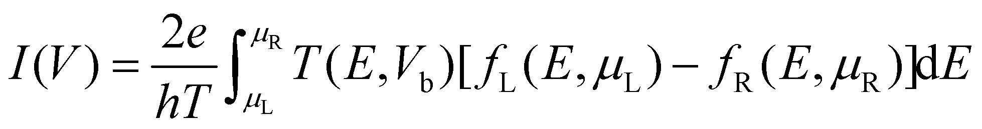
The optimized structure of MoS2, as shown in Fig. 1a and inset of Fig. 1c, demonstrates a Mo–S bond length of 2.414 Å and a S–Mo–S bond angle of 80.702°, together with a minimum Mo–Mo distance of 3.19 Å consistent with reported results.41 In the case of V-MoS2, where V is trigonal-prismatically coordinated (Fig. 1d), the less electronegativity of V compared to Mo contributes to greater polarization of the V–S bonds, resulting in reduced bond length of 2.365 Å and increased S–V–S bond angle of 80.893°, also in agreement with previous reports.42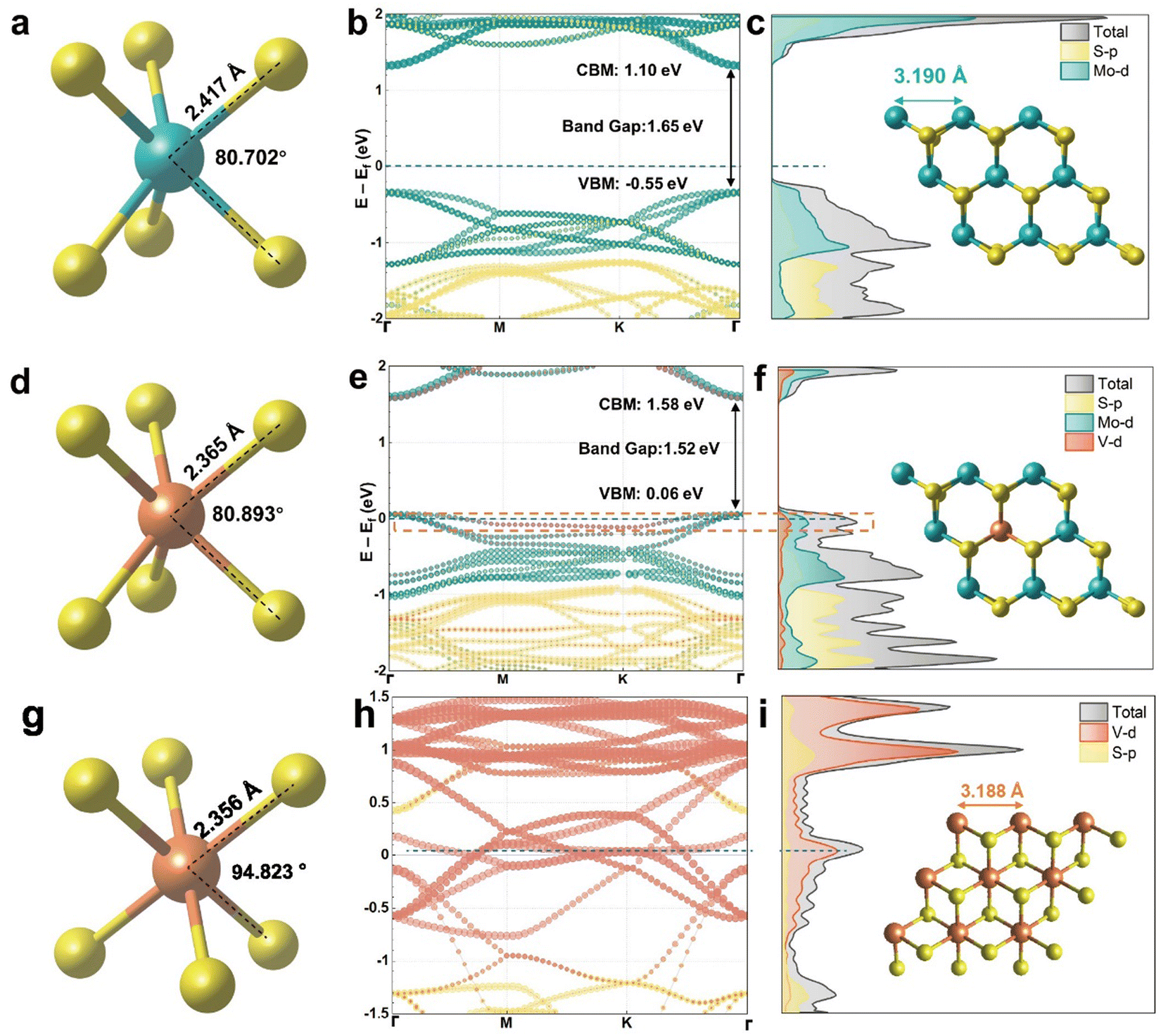 | ||
| Fig. 1 Crystal structure and electronic properties. Atomic structures of MoS2 (a), V-MoS2 (d), and VS2 (g) are schematically illustrated, showing the S-M bond length and the S-M-S bond angle, where M represents Mo or V. The Mo, V, and S atoms are shown in blue, orange, and yellow, respectively. Band structures and PDOS of MoS2 (b) and (c), V-MoS2 (e) and (f), and VS2 (h) and (i) are also presented. The insets in the PDOS spectra correspond to the respective crystal cell models. | ||
To verify the p-type doping effect of V dopants, we calculated the projected band structures and projected densities of states (PDOS) for both pristine MoS2 and V-MoS2. The pristine MoS2 exhibits fully occupied valence band and an intrinsic bandgap of 1.65 eV, whose band edges mainly originate from the non-bonding d orbitals of Mo atoms (Fig. 1b and c). In contrast, the V-MoS2 shows prominent features of a p-type semiconductor, with the Fermi level (EF) slightly intersects the valence band (Fig. 1e and f). Notably, our orbital projection analysis further reveals that the topmost valence band mainly originates from the V atom and contributes to a pronounced peak at EF in the PDOS spectra, as marked by the dash orange box in Fig. 1e and f. It is foreseeable that in V-MoS2 short-channel transistors, the presence of this conspicuous doping peak will exert a noteworthy influence on the charge transport properties, which is the focus of the present work.
In addition, 1T-VS2, an air-stable metallic 2D material,43 has also been modeled and theoretically calculated. As shown in Fig. 1g and inset of Fig. 1i, the optimized structure of VS2 exhibits lattice parameters consistent with literature reports44 and close to that of MoS2. Band structure and PDOS analyses of VS2 (Fig. 1h and i) reveal no bandgap and a high density of states at EF, confirming its metallic property. For now, we are ready to investigate the short-channel transport properties of pristine MoS2 and V-MoS2, using VS2 as the electrode material.
The configuration of the FET device is illustrated in Fig. 2a. Two semi-infinitely long 1T-VS2 electrodes were utilized, ensuring that the electrode region maintains a macroscopic potential under the shielding approximation. The central region is composed of V-MoS2, which exhibits a finite size along the transport direction, satisfying the short-channel condition. One-dimensional in-plane periodic boundary conditions were imposed perpendicular to the transport direction to eliminate edge effects. Sufficient buffer layers were introduced between the channel and the electrodes to ascertain the wavefunction continuity at the channel/electrode interface, which was further confirmed by the potential profile analysis (Fig. S2, ESI†). Additionally, two virtual gate electrodes with an equivalent oxide thickness of 0.5 nm were placed above and below the central region to modulate the EF of the channel material.
 | ||
| Fig. 2 Schematic diagram of a FET model with VS2 electrodes at both ends, V-MoS2 channel in the middle (Lch =3.0 nm), and gate electrodes (EOT = 0.5 nm) on top and bottom (a). The real-space DOS at −0.2 eV (b) and corresponding 2D plot (c) are shown with zero source-drain bias applied. The inset in (b) represents the differential charge density at the V-doped site. | ||
As depicted in Fig. 2b and c, we firstly calculated the real-space DOS (@ −0.2 eV) of the V-MoS2 transistor (Lch = 3.0 nm) to gain insights into its electronic characteristics. The localized nature of the V-doping state with a spanning size of ∼0.8 nm can be clearly visualized, showing finite influence only on the six nearest-neighboring Mo atoms. Corresponding PDOS profile of the device also verified the localization of the doping state, which is absent in pristine MoS2 (Fig. S3, ESI†). By plotting the differential charge density around the V dopant (inset of Fig. 2b), it is evident that the V atom undergoes electron exchange with three nearest S atoms and six second-nearest Mo atoms, whilst the third-nearest S atoms are barely affected. Besides, the differential charge density of the Mo atoms exhibits a similar pattern to the LDOS distribution (highlighted by the red box in Fig. 2b and c), possibly suggesting that direct d orbital hybridization is responsible for the finite spanning of the V-doping state.
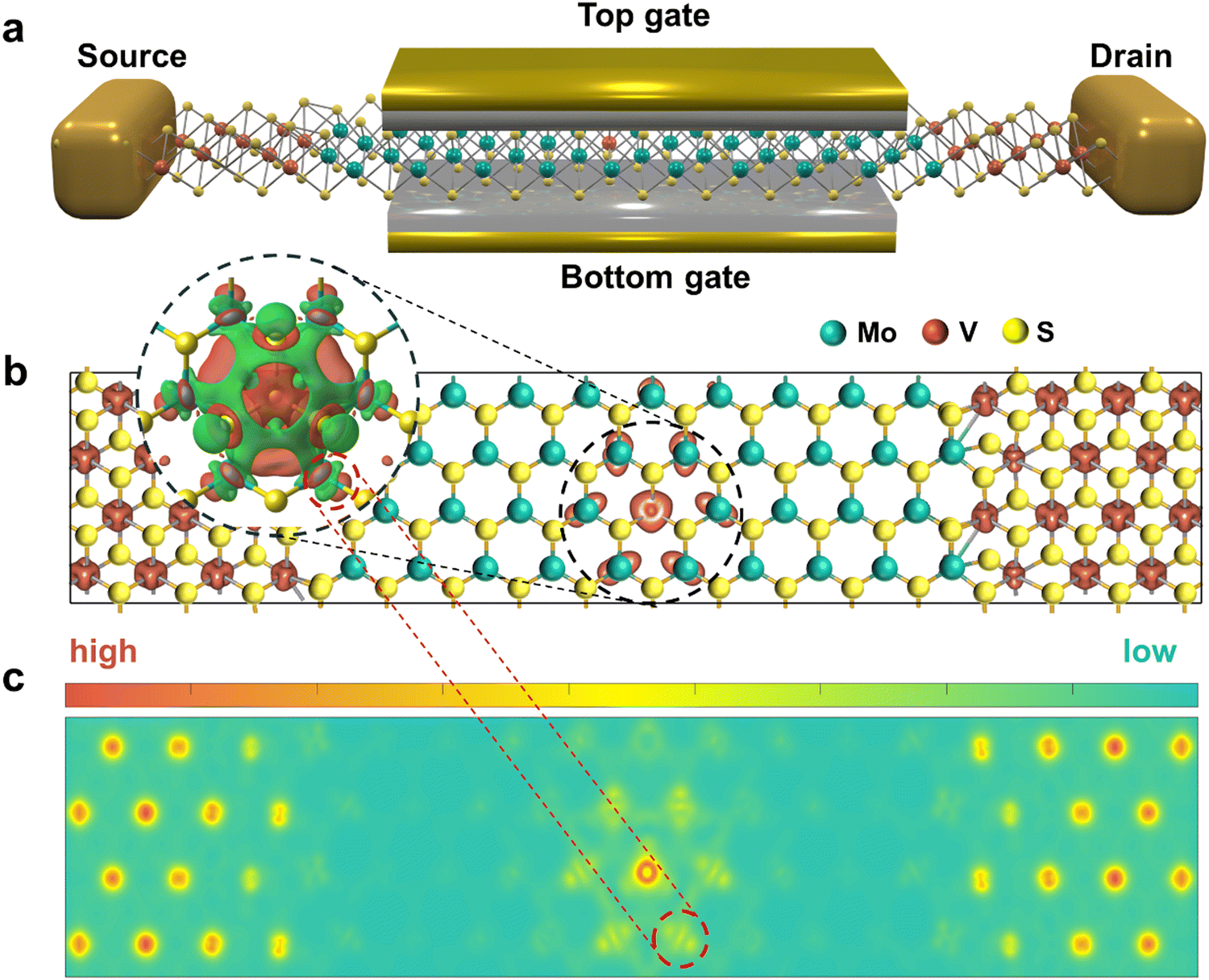
The contact characteristics are of critical importance for device transport.45 As shown in Fig. S4 (ESI†), the interface between VS2 and MoS2 manifests a p-type Schottky contact, exhibiting a Schottky barrier height of 0.63 eV, whereas the heterojunction formed between V-MoS2 and VS2 displays a quasi–Ohmic contact. Detailed discussion on the contact properties is provided in ESI.† To comprehensively investigate the doping effect on short-channel charge transport, a series of V-MoS2 transistors were constructed and simulated, with varied Lch ranging from 1.2 nm to 4.2 nm (Fig. 3a–f). A bias voltage of 0.2 V was applied to the source electrodes to drive the current flow across the channels. For comparison, devices with pristine MoS2 channels were also simulated. The transfer curves for all the devices clearly demonstrate the p-type doping effect of V atoms on MoS2, as evidenced by higher hole conductance at Vg = 0 V compared to pristine MoS2. At smallest Lch of 1.2 nm and 1.8 nm, the smooth transfer curves (Fig. 3a and b), combined with the higher on-state currents of V-MoS2 compared to pristine MoS2, suggest an efficient source-drain tunneling and the absence of charge scattering at the V-doped site. Notably, at intermediate Lch of 2.4 nm and 3.0 nm, discernible current bulges appear in the subthreshold regions (indicated by the dash lines in Fig. 3c and d), likely associated with the existence of localized V-doping states. Similar dome-shaped transport characteristics have been experimentally observed in V-doped WSe2 monolayers,46 where the presence of V impurity states near the valence-band edge was also inferred as the key factor. Our transport simulation hence captures the essential characteristics of doped 2D systems, hinting on new device physics at ultimate length scales.
 | ||
| Fig. 3 (a)–(f) Transfer characteristics of MoS2 (hollow circles) and V-MoS2 (solid spheres) at Lch = 1.2 nm (a), 1.8 nm (b), 2.4 nm (c), 3.0 nm (d), 3.6 nm (e), and 4.2 nm (f), under a source bias of 0.2 V. Shown in (g-i) are the comparison of the on-state currents (g), off-state currents (h), and on/off ratios (i) between V-MoS2 (orange) and MoS2 (cyan) at different Lch. | ||
However, with the Lch further increased, the bulging feature for V-MoS2 was concealed by current fluctuations (Fig. 3e and f), along with the reduced on-state currents (Fig. 3g). While the off-state currents for both V-MoS2 and MoS2 transistors show similar monotonic evolution depending on Lch (Fig. 3h), the decrease of on-state currents for V-MoS2 leads to a saturation behavior in the on/off ratios (Fig. 3i), highly suggesting that charge scattering predominantly affects the transport properties of V-MoS2 at these channel lengths. A detailed physical picture was elucidated in the context of random telegraph noise47,48 for short-channel MoS2 transistors, which incorporated the dynamics of charge capture and emission by unspecified atomic defects. Besides, subthreshold swings and field-effect mobilities of both the V-MoS2 and MoS2 transistors at different channel lengths were extracted from the simulated transfer curves in Fig. 3a–f, which further highlight the electronic role of V dopants (Fig. S5, ESI†). Overall, our first-principles calculations reveal an Lch-dependent electronic effect associated with the V dopants, contributing to anomalous current peaks at intermediate Lch, while causing scattering of charge carriers at Lch ≥ 3.6 nm.
Since charge scattering by atomic impurities is a well-recognized phenomenon, we mainly focus on illustrating the origin of the anomalous current peak in the subthreshold region. For this purpose, the V-MoS2 transistor with Lch = 3.0 nm was further elucidated by the PDOS profiles (Fig. S6, ESI†) and corresponding transmission spectra (Fig. S7, ESI†), under a constant source-drain bias (Vsd = 0.2 V) and varied gate voltages (Vg). We note that only those transmission coefficients within the bias window of −0.2 eV to 0 eV contribute to the source-drain current.
At Vg = 0.7 V, the bias window intersects the bandgap, providing no states in the channel to accommodate charge carriers. Due to the sufficient Lch, direct source-drain tunneling was inhibited, leading to small integrated transmission probability and an “off-state” of the device, as depicted in Fig. 4a. As Vg gradually decreased, the energy bands of the channel material underwent continuous elevation, causing the bias window to overlap with the V-doping state at Vg = 0 V (Fig. 4b). The relatively short distance between the dopant and the electrodes (half of the Lch) facilitated effective tunneling, allowing the dopant site to act as a “relay station” for charge carriers. This contributes to a “high-transmission state” from the source to the drain, manifesting a conductance peak in the subthreshold region (Fig. 3d), a phenomenon we refer to as “assisted tunneling”.
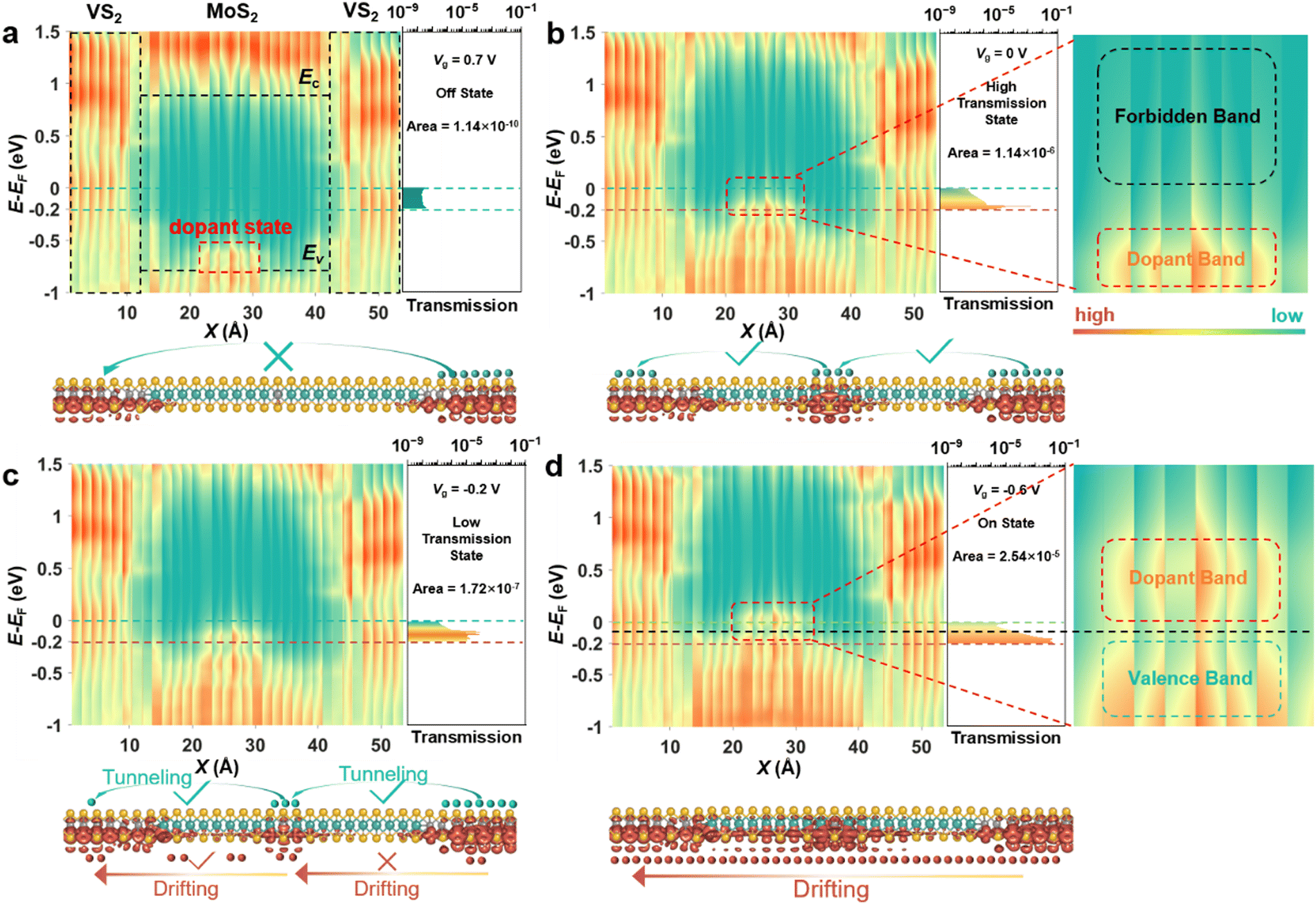 | ||
| Fig. 4 PDOS profiles, electron transmission spectra, and real-space DOS at -0.2 eV of a V-MoS2 transistor, with Lch = 3.0 nm and Vsd = 0.2 V, calculated under different gate voltages (Vg) of 0.7 V (a), 0 V (b), −0.2 V (c), and −0.6 V. Insets on the right of (b) and (d) show magnified views of the forbidden band, the dopant band, and the valence band in the PDOS profiles. The orange arrows (balls) indicate drift transport (holes), while the cyan arrows (balls) denote tunneling transport (holes). | ||
However, as Vg further decreased to −0.2 V, the integrated transmission probability diminished from 1.14 × 10⁻⁶ (at Vg = 0 V) to 1.72 × 10⁻⁷ (Fig. 4c). This behavior arises from the dual functionality of the V-doping site, which not only facilitates assisted tunneling but also induces charge scattering, as illustrated by the real-space DOS image in Fig. 4c. Specifically, at Vg = −0.2 V, holes around the V atom accumulated by the gating effect depleted the localized doping state and repelled positive charges, thereby preventing to some extent carrier tunneling from the source to the dopant. Even though drift transport occurred from the dopant to the drain, the overall channel conductance decreased, resulting in a “low-transmission state” and the inflection point observed in the transfer curve (Fig. 3d). With Vg decreased to −0.6 V, the valence band of the MoS2 channel started to enter the bias window, enabling carriers to drift through the entire channel and transitioning the device into the “on-state” (Fig. 4d). In this case, the V-doping site with enriched and trapped holes acted as a charge scattering center, reducing the on-state currents compared to pristine MoS2.
Schematic band diagrams are plotted in Fig. 5 to further elucidate the electronic functionalities of V-doped states at different channel lengths. As depicted in Fig. 5a and b, when the channel length is less than 1.8 nm, the carriers can tunnel directly between the two electrodes, and the V-doped states play a supporting role on enhancing the tunneling probability. When the channel length is in the range of 2.4–3.0 nm (Fig. 5c and d), direct carrier tunneling between the electrodes is suppressed; in this case, the V-doped sites act as “repeaters” that facilitate assisted tunneling, leading to an anomalous transconductance peak in the subthreshold region. Importantly, even considering spin polarization of the dopant states, the assisted-tunneling effect was still valid, manifesting two kinks in the subthreshold region that can be ascribed to the Coulomb splitting effect of the spin-polarized state.49 When the channel length exceeds 3.6 nm (Fig. 5e and f), the V-doped sites can no longer afford assisted tunneling, and instead, they act as impurity scattering centers that imped the carrier transport.
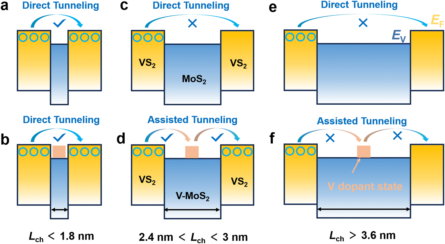 | ||
| Fig. 5 Schematic illustration on the electronic functionalities of the V-doped states at different channel lengths. Band diagrams of MoS2 and V-MoS2 at Lch < 1.8 nm (a, b), 2.4 nm < Lch < 3.0 nm (c, d) and Lch > 3.6 nm (e) and (f) are plotted. The blue hollow circles represent holes. The yellow and blue regions signify the VS2 electrodes and the MoS2 channel, respectively. The orange regions represent the V-doped states at the top of the MoS2 valence band. | ||
Conclusion
In summary, we have uncovered the electronic effects of heteroatom dopants in short-channel 2D transistors, using a combination of first-principles calculations and quantum transport simulations. By employing lateral VS2–MoS2–VS2 heterostructures as the model system, we show that the implanted V dopants in the MoS2 channels manifest dual electronic functionalities, either promoting source-drain currents through assisted tunneling, or acting as scattering centers to reduce the channel conductance. The trade-off of the two competing electronic effects can be modulated by varying the channel lengths in the sub-10 nm range. Such Lch-dependent electronic functionalities differ from the known mechanisms of carrier doping and impurity scattering22 caused by point defects, offering possibility of designed electronics at these extreme length scales, such as atomic Boltzmann machines50 and dopant-atom networks.51Data availability
The authors confirm that the data supporting the findings of this study are available within the article and its ESI.†Conflicts of interest
There are no conflicts to declare.Acknowledgements
This work was financially supported by the National Natural Science Foundation of China (22205142) and the Science and Technology Commission of Shanghai Municipality (21ZR1442100, 21PJ1410200). The work was also supported by the Startup Fund and the Double First-Class Initiative Fund of ShanghaiTech University.References
- R. Chau, B. Doyle, S. Datta, J. Kavalieros and K. Zhang, Integrated nanoelectronics for the future, Nat. Mater., 2007, 6, 810–812 CrossRef CAS PubMed.
- T. N. Theis and P. M. Solomon, It's Time to Reinvent the Transistor, Science, 2010, 327, 1600–1601 CrossRef CAS PubMed.
- A. D. Franklin, Nanomaterials in transistors: From high-performance to thin-film applications, Science, 2015, 349, aab2750 CrossRef PubMed.
- D. Akinwande, C. Huyghebaert, C.-H. Wang, M. I. Serna, S. Goossens, L.-J. Li, H. S. P. Wong and F. H. L. Koppens, Graphene and two-dimensional materials for silicon technology, Nature, 2019, 573, 507–518 CrossRef CAS PubMed.
- B. Radisavljevic, A. Radenovic, J. Brivio, V. Giacometti and A. Kis, Single-layer MoS2 transistors, Nat. Nanotechnol., 2011, 6, 147–150 CrossRef CAS PubMed.
- M. Chhowalla, D. Jena and H. Zhang, Two-dimensional semiconductors for transistors, Nat. Rev. Mater., 2016, 1, 16052 CrossRef CAS.
- Y. Liu, X. Duan, H.-J. Shin, S. Park, Y. Huang and X. Duan, Promises and prospects of two-dimensional transistors, Nature, 2021, 591, 43–53 CrossRef CAS PubMed.
- S. B. Desai, S. R. Madhvapathy, A. B. Sachid, J. P. Llinas, Q. Wang, G. H. Ahn, G. Pitner, M. J. Kim, J. Bokor, C. Hu, H. S. P. Wong and A. Javey, MoS2 transistors with 1-nanometer gate lengths, Science, 2016, 354, 99–102 CrossRef CAS.
- F. Wu, H. Tian, Y. Shen, Z. Hou, J. Ren, G. Gou, Y. Sun, Y. Yang and T.-L. Ren, Vertical MoS2 transistors with sub-1-nm gate lengths, Nature, 2022, 603, 259–264 CrossRef CAS PubMed.
- S. Chuang, C. Battaglia, A. Azcatl, S. McDonnell, J. S. Kang, X. Yin, M. Tosun, R. Kapadia, H. Fang, R. M. Wallace and A. Javey, MoS2 P-type Transistors and Diodes Enabled by High Work Function MoOx Contacts, Nano Lett., 2014, 14, 1337–1342 CrossRef CAS.
- C. Dorow, K. O’Brien, C. H. Naylor, S. Lee, A. Penumatcha, A. Hsiao, T. Tronic, M. Christenson, K. Maxey, H. Zhu, A. Oni, U. Alaan, T. Gosavi, A. S. Gupta, R. Bristol, S. Clendenning, M. Metz and U. Avci, Advancing Monolayer 2-D nMOS and pMOS Transistor Integration From Growth to van der Waals Interface Engineering for Ultimate CMOS Scaling, IEEE Trans. Electron Devices, 2021, 68, 6592–6598 CAS.
- Y. Wang, J. C. Kim, Y. Li, K. Y. Ma, S. Hong, M. Kim, H. S. Shin, H. Y. Jeong and M. Chhowalla, P-type electrical contacts for 2D transition-metal dichalcogenides, Nature, 2022, 610, 61–66 CrossRef.
- H. Gao, J. Suh, M. C. Cao, A. Y. Joe, F. Mujid, K.-H. Lee, S. Xie, P. Poddar, J.-U. Lee, K. Kang, P. Kim, D. A. Muller and J. Park, Tuning Electrical Conductance of MoS2 Monolayers through Substitutional Doping, Nano Lett., 2020, 20, 4095–4101 CrossRef CAS.
- Y.-C. Lin, R. Torsi, D. B. Geohegan, J. A. Robinson and K. Xiao, Controllable Thin-Film Approaches for Doping and Alloying Transition Metal Dichalcogenides Monolayers, Adv. Sci., 2021, 8, 2004249 CrossRef CAS.
- A. Kozhakhmetov, S. Stolz, A. M. Z. Tan, R. Pendurthi, S. Bachu, F. Turker, N. Alem, J. Kachian, S. Das, R. G. Hennig, O. Gröning, B. Schuler and J. A. Robinson, Controllable p-Type Doping of 2D WSe2 via Vanadium Substitution, Adv. Funct. Mater., 2021, 31, 2105252 CrossRef CAS.
- J. Suh, T. L. Tan, W. Zhao, J. Park, D.-Y. Lin, T.-E. Park, J. Kim, C. Jin, N. Saigal, S. Ghosh, Z. M. Wong, Y. Chen, F. Wang, W. Walukiewicz, G. Eda and J. Wu, Reconfiguring crystal and electronic structures of MoS2 by substitutional doping, Nat. Commun., 2018, 9, 199 CrossRef.
- L. Zhang, G. Wang, Y. Zhang, Z. Cao, Y. Wang, T. Cao, C. Wang, B. Cheng, W. Zhang, X. Wan, J. Lin, S.-J. Liang and F. Miao, Tuning Electrical Conductance in Bilayer MoS2 through Defect-Mediated Interlayer Chemical Bonding, ACS Nano, 2020, 14, 10265–10275 CrossRef CAS PubMed.
- J. Zhang, Y. Zhu, M. Tebyetekerwa, D. Li, D. Liu, W. Lei, L. Wang, Y. Zhang and Y. Lu, Vanadium-Doped Monolayer MoS2 with Tunable Optical Properties for Field-Effect Transistors, ACS Appl. Nano Mater., 2021, 4, 769–777 CrossRef CAS.
- M. Li, X. Wu, W. Guo, Y. Liu, C. Xiao, T. Ou, Y. Zheng and Y. Wang, Controllable p-type doping of monolayer MoS2 with tantalum by one-step chemical vapor deposition, J. Mater. Chem. C, 2022, 10, 7662–7673 RSC.
- Z. Wang, M. Tripathi, Z. Golsanamlou, P. Kumari, G. Lovarelli, F. Mazziotti, D. Logoteta, G. Fiori, L. Sementa, G. M. Marega, H. G. Ji, Y. Zhao, A. Radenovic, G. Iannaccone, A. Fortunelli and A. Kis, Substitutional p-Type Doping in NbS2–MoS2 Lateral Heterostructures Grown by MOCVD, Adv. Mater., 2023, 35, 2209371 CrossRef CAS PubMed.
- J.-Y. Noh, H. Kim, M. Park and Y.-S. Kim, Deep-to-shallow level transition of Re and Nb dopants in monolayer MoS2 with dielectric environments, Phys. Rev. B: Condens. Matter Mater. Phys., 2015, 92, 115431 CrossRef.
- S. T. Pantelides, The electronic structure of impurities and other point defects in semiconductors, Rev. Mod. Phys., 1978, 50, 797–858 CrossRef CAS.
- E. Kamieniecki, Effect of charge trapping on effective carrier lifetime in compound semiconductors: High resistivity CdZnTe, J. Appl. Phys., 2014, 116, 193702 CrossRef.
- M. Fuechsle, J. A. Miwa, S. Mahapatra, H. Ryu, S. Lee, O. Warschkow, L. C. L. Hollenberg, G. Klimeck and M. Y. Simmons, A single-atom transistor, Nat. Nanotechnol., 2012, 7, 242–246 CrossRef CAS.
- W. S. Leong, Q. Ji, N. Mao, Y. Han, H. Wang, A. J. Goodman, A. Vignon, C. Su, Y. Guo, P.-C. Shen, Z. Gao, D. A. Muller, W. A. Tisdale and J. Kong, Synthetic Lateral Metal-Semiconductor Heterostructures of Transition Metal Disulfides, J. Am. Chem. Soc., 2018, 140, 12354–12358 CrossRef CAS PubMed.
- Y. Yoon, K. Ganapathi and S. Salahuddin, How Good Can Monolayer MoS2 Transistors Be, Nano Lett., 2011, 11, 3768–3773 CrossRef CAS.
- D. Marian, E. Dib, T. Cusati, E. G. Marin, A. Fortunelli, G. Iannaccone and G. Fiori, Transistor Concepts Based on Lateral Heterostructures of Metallic and Semiconducting Phases of MoS2, Phys. Rev. Appl., 2017, 8, 054047 CrossRef.
- Y. Zhao, Y. Li and F. Ma, Performance Upper Limit of Sub-10 nm Monolayer MoS2 Transistors with MoS2–Mo Electrodes, J. Phys. Chem. C, 2022, 126, 12100–12112 CrossRef CAS.
- Z.-Q. Fan, X.-W. Jiang, J.-W. Luo, L.-Y. Jiao, R. Huang, S.-S. Li and L.-W. Wang, In-plane Schottky-barrier field-effect transistors based on 1T/2H heterojunctions of transition-metal dichalcogenides, Phys. Rev. B, 2017, 96, 165402 CrossRef.
- H. Lü, Y. Zhang, X. Liu, Y. Wang, Q. Zhang and H. Yin, Theoretical limit of how small we can make MoS2 transistor channels, J. Phys. D, 2022, 55, 105304 CrossRef.
- Hongzhiwei Technology, Device Studio, Version 2023A, China, 2023, https://cloud.hzwtech.com.
- G. Kresse and D. Joubert, From ultrasoft pseudopotentials to the projector augmented-wave method, Phys. Rev. B: Condens. Matter Mater. Phys., 1999, 59, 1758–1775 CrossRef CAS.
- P. E. Blöchl, Projector augmented-wave method, Phys. Rev. B: Condens. Matter Mater. Phys., 1994, 50, 17953–17979 CrossRef.
- J. Taylor, H. Guo and J. Wang, Ab initio modeling of quantum transport properties of molecular electronic devices, Phys. Rev. B: Condens. Matter Mater. Phys., 2001, 63, 245407 CrossRef.
- J. P. Perdew and W. Yue, Accurate and simple density functional for the electronic exchange energy: Generalized gradient approximation, Phys. Rev. B, 1986, 33, 8800–8802 CrossRef.
- J. P. Perdew, J. A. Chevary, S. H. Vosko, K. A. Jackson, M. R. Pederson, D. J. Singh and C. Fiolhais, Atoms, molecules, solids, and surfaces: Applications of the generalized gradient approximation for exchange and correlation, Phys. Rev. B: Condens. Matter Mater. Phys., 1992, 46, 6671–6687 CrossRef CAS PubMed.
- M. Brandbyge, J.-L. Mozos, P. Ordejón, J. Taylor and K. Stokbro, Density-functional method for nonequilibrium electron transport, Phys. Rev. B: Condens. Matter Mater. Phys., 2002, 65, 165401 CrossRef.
- H. J. Monkhorst and J. D. Pack, Special points for Brillouin-zone integrations, Phys. Rev. B: Solid State, 1976, 13, 5188–5192 CrossRef.
- M. Büttiker, Y. Imry, R. Landauer and S. Pinhas, Generalized many-channel conductance formula with application to small rings, Phys. Rev. B: Condens. Matter Mater. Phys., 1985, 31, 6207–6215 CrossRef PubMed.
- Y. Zhang, X. Chen, Y. Huang, C. Zhang, F. Li and H. Shu, The Role of Intrinsic Defects in Electrocatalytic Activity of Monolayer VS2 Basal Planes for the Hydrogen Evolution Reaction, J. Phys. Chem. C, 2017, 121, 1530–1536 CrossRef CAS.
- D. Yang, J. Jiang, J. Chen, X. Guo, X. Yang, X. Zheng, C. Deng, H. Xie, F. Song, F. Ouyang, X. Yuan, M. Chen and H. Huang, In-plane anisotropy in van der Waals epitaxial MoS2 on MoO2(010), Appl. Phys. Lett., 2023, 122, 111602 CrossRef CAS.
- I. Williamson, S. Li, A. Correa Hernandez, M. Lawson, Y. Chen and L. Li, Structural, electrical, phonon, and optical properties of Ti- and V-doped two-dimensional MoS2, Chem. Phys. Lett., 2017, 674, 157–163 CrossRef CAS.
- Q. Ji, C. Li, J. Wang, J. Niu, Y. Gong, Z. Zhang, Q. Fang, Y. Zhang, J. Shi, L. Liao, X. Wu, L. Gu, Z. Liu and Y. Zhang, Metallic Vanadium Disulfide Nanosheets as a Platform Material for Multifunctional Electrode Applications, Nano Lett., 2017, 17, 4908–4916 CrossRef CAS PubMed.
- Y. Ma, Y. Dai, M. Guo, C. Niu, Y. Zhu and B. Huang, Evidence of the Existence of Magnetism in Pristine VX2 Monolayers (X = S, Se) and Their Strain-Induced Tunable Magnetic Properties, ACS Nano, 2012, 6, 1695–1701 CrossRef CAS.
- Y. Li, L. Su, Y. Lu, Q. Luo, P. Liang, H. Shu and X. Chen, High-throughput screening of phase-engineered atomically thin transition-metal dichalcogenides for van der Waals contacts at the Schottky–Mott limit, InfoMat, 2023, 5, e12407 CrossRef CAS.
- B. Song, S. J. Yun, J. Jiang, J. Avila, K. Beach, W. Choi, Y.-M. Kim, D. Yoon, H. Terrones, Y. J. Song, M. C. Asensio, D. L. Duong and Y. H. Lee, Evidence of itinerant holes for long-range magnetic order in the tungsten diselenide semiconductor with vanadium dopants, Phys. Rev. B, 2021, 103, 094432 CrossRef CAS.
- B. Stampfer, F. Zhang, Y. Y. Illarionov, T. Knobloch, P. Wu, M. Waltl, A. Grill, J. Appenzeller and T. Grasser, Characterization of Single Defects in Ultrascaled MoS2 Field-Effect Transistors, ACS Nano, 2018, 12, 5368–5375 CrossRef CAS PubMed.
- H. Ravichandran, T. Knobloch, A. Pannone, A. Karl, B. Stampfer, D. Waldhoer, Y. Zheng, N. U. Sakib, M. U. Karim Sadaf, R. Pendurthi, R. Torsi, J. A. Robinson, T. Grasser and S. Das, Observation of Rich Defect Dynamics in Monolayer MoS2, ACS Nano, 2023, 17, 14449–14460 CrossRef CAS PubMed.
- H. González-Herrero, J. M. Gómez-Rodríguez, P. Mallet, M. Moaied, J. J. Palacios, C. Salgado, M. M. Ugeda, J.-Y. Veuillen, F. Yndurain and I. Brihuega, Atomic-scale control of graphene magnetism by using hydrogen atoms, Science, 2016, 352, 437–441 CrossRef PubMed.
- B. Kiraly, E. J. Knol, W. M. J. van Weerdenburg, H. J. Kappen and A. A. Khajetoorians, An atomic Boltzmann machine capable of self-adaption, Nat. Nanotechnol., 2021, 16, 414–420 CrossRef CAS PubMed.
- T. Chen, J. van Gelder, B. van de Ven, S. V. Amitonov, B. de Wilde, H.-C. Ruiz Euler, H. Broersma, P. A. Bobbert, F. A. Zwanenburg and W. G. van der Wiel, Classification with a disordered dopant-atom network in silicon, Nature, 2020, 577, 341–345 CrossRef CAS.
Footnotes |
| † Electronic supplementary information (ESI) available. See DOI: https://doi.org/10.1039/d4qm00494a |
| ‡ These authors contribute equally to this work. |
| This journal is © the Partner Organisations 2024 |