
Advanced inorganic nanomaterials for high-performance electrochromic applications
Zekun
Huang†
ab,
Liping
Feng†
b,
Xianjie
Xia†
b,
Jing
Zhao
b,
Penglu
Qi
b,
Yiting
Wang
b,
Junhua
Zhou
b,
Laifa
Shen
 ab,
Shengliang
Zhang
*ab and
Xiaogang
Zhang
*ab
ab,
Shengliang
Zhang
*ab and
Xiaogang
Zhang
*ab
aState Key Laboratory of Mechanics and Control for Aerospace Structures, Nanjing University of Aeronautics and Astronautics, No. 29 Yudao Street, Nanjing 210016, China. E-mail: zhangsl@nuaa.edu.cn; azhangxg@nuaa.edu.cn
bJiangsu Key Laboratory of Electrochemical Energy Storage Technologies, College of Materials Science and Technology, Nanjing University of Aeronautics and Astronautics, Nanjing 210016, China
First published on 29th December 2023
Abstract
Electrochromic materials and devices with the capability of dynamic optical regulation have attracted considerable attention recently and have shown a variety of potential applications including energy-efficient smart windows, multicolor displays, atuto-diming mirrors, military camouflage, and adaptive thermal management due to the advantages of active control, wide wavelength modulation, and low energy consumption. However, its development still experiences a number of issues such as long response time and inadequate durability. Nanostructuring has demonstrated that it is an effective strategy to improve the electrochromic performance of the materials due to the increased reaction active sites and the reduced ion diffusion distance. Various advanced inorganic nanomaterials with high electrochromic performance have been developed recently, significantly contributing to the development of electrochromic applications. In this review, we systematically introduce and discuss the recent advances in advanced inorganic nanomaterials including zero-, one-, and two-dimensional materials for high-performance electrochromic applications. Finally, we outline the current major challenges and our perspectives for the future development of nanostructured electrochromic materials and applications.
 Shengliang Zhang | Shengliang Zhang is Associate Professor at the College of Materials Science and Technology, Nanjing University of Aeronautics and Astronautics. He received his Ph.D. degree from the National University of Singapore in 2019. He then started his postdoctoral research at the National University of Singapore between 2019 and 2020. His current research interests include electrochromic materials and devices, multi-spectral adaptive camouflage, and intelligent photothermal regulation. |
1. Introduction
Electrochromism is the phenomenon where optical properties (transmittance, absorbance, reflectance, or emittance) of a material are dynamically and reversibly changed by the application of a small external electric field.1,2 This preeminent technology has shown a variety of potential applications including energy-efficient smart windows,3–10 multicolor displays,11–13 atuto-diming mirrors, military camouflage,14–16 and adaptive thermal management17–19 (Fig. 1) due to the advantages of active control, wide wavelength modulation, and low energy consumption. Therefore, electrochromic (EC) materials and devices have attracted increasing attention from scientific and industrial communities and have become a hot research topic in recent years. | ||
| Fig. 1 Schematic diagram of inorganic electrochromic nanomaterials and their promising applications. | ||
An EC device typically comprises an EC layer on a conductive electrode, an electrolyte layer, and an ion storage layer on a conductive electrode.1,2 The mechanism of electrochromism can be attributed to the ions and electrons that are injected/extracted into/from the EC materials under an applied voltage, resulting in the redox reaction of materials and reversible changes in optical properties.20–24 The optical modulation, switching time, coloration efficiency, bistability, cycling stability, and energy consumption are the main evaluating parameters of EC materials and devices.
For an EC device, the EC materials are undoubtedly the core components, playing the key function of dynamically tuning the optical properties. Generally, EC materials can be divided into organic materials and inorganic materials.20–22 Organic EC materials mainly include organic small molecules (viologen and its derivatives)25 and conducting polymers (e.g., polyaniline, polythiophene, polypyrrole, and their derivatives).17,26–28 The organic EC materials stand out due to their multicolor tunability, fast response, flexibility, structural modifiability, and easy processing, which endow them wide potential applications, especially in displays and wearable devices. Recently, inorganic EC materials have also been widely investigated because of their excellent stability, wide range of working temperature, and wide spectral modulation.29–31 Transition metal oxides32–36 (e.g., WO3, MoO3, TiO2, NiO, and V2O5), Prussian blue (PB),37,38 and carbon materials18,19 are typical inorganic EC materials. Due to the high optical modulation and high stability against high temperature and strong light, inorganic EC materials have been suggested as the most suitable materials for smart windows and thermal management in some extreme application environments.
Although inorganic EC materials have shown a number of advantages, the slow switching speed is the major issue and hinders their practical applications. Based on the mechanism of electrochromism, the response time is related with the ion diffusion kinetics and ion diffusion distance in electrochromic materials. Nanostructuring is therefore an effective strategy to improve the switching speed of the materials due to the increased ion diffusion speed and the reduced ion diffusion distance.29–31 In addition, nanomaterials usually have a high surface area, which could accommodate more ions and then increase the optical modulation. Moreover, nanostructuring can also alleviate the volume expansion during ion intercalation and reduce the possibility of ion-trapping in EC materials, which is clearly beneficial for enhancing the cycling stability. Consequently, lots of advanced inorganic nanomaterials with high electrochromic performance have been developed, especially in the last 5 years,39–47 which notably contributes to the development of electrochromic applications.
Although a few literature reviews on electrochromic materials and devices have been reported,29–31 there is a strong demand for a timely and updated comprehensive overview of recent progress (especically in the near 3 years) on advanced inorganic nanomaterials for high-performance electrochromic applications. In this review, we systematically introduce and discuss the recent advances in advanced inorganic electrochromic nanomaterials including zero dimensional (0D) materials (nanoparticles and quantum dots), one dimensional (1D) materials (nanowires and nanorods), and two dimensional (2D) materials. Finally, we outline the current major challenges and our perspectives for the future development of nanostructured inorganic electrochromic materials and applications. We hope that this review provides readers with a systematic perspective on advanced inorganic electrochromic nanomaterials, promoting the development of electrochromic fields.
2. Inorganic nanomaterials for EC devices
2.1. Zero dimensional (0D) inorganic EC materials
Zero dimensional (0D) nanomaterials mainly refer to nanoparticles and quantum dots, which are at the nanometer level in all three dimensions. Therefore, 0D nanomaterials can notably reduce the ion diffusion distance and increase the ion diffusion speed and ion storage sites, significantly improving the EC performance of inorganic materials. In the following content, we mainly introduce and discuss the recent progress on 0D transition metal oxides. | ||
| Fig. 2 (a) TEM image of WO3−x nanoparticles. (b) SEM image of WO3−x-NbOx nanocomposite. (c) Transmittance spectra of the WO3−x-NbOx composite film at different applied potentials and the corresponding photos of the sample. (a–c) Adapted with permission from ref. 36. Copyright 2015, American Chemical Society. (d) SEM image of the Ti-WO3 film. (e) XPS spectra of W 4f. (f) Optical transmittance spectra of the Ti-WO3 film before and after 1000 cycles. (g) Optical transmittance of the assembled device at different applied voltages. (h) Simulation of sunshine in the home-built test system. (i) Digital photo of the device under natural light. Infrared thermography images and temperature of the device in the bright (j), cool (k), and dark (l) modes after the AM 1.5 sunlight simulator is irradiated for the same time. (d–l) Adapted with permission from ref. 48. Copyright 2022, Elsevier. | ||
Doping is an efficient method to improve the performance and adjust the nanostructures of WO3. Recently, Cao et al. reported a porous Ti-doped WO3 nanoparticle film (Fig. 2d) prepared by the facile sol–gel method with polyvinylpyrrolidone (PVP) as the foaming agent.48 Because of the existence of Ti4+ in the WO3 host, it can change the crystalline phase of WO3 from the monoclinic to cubic phase. It also can prevent repeated crystal transformation (monoclinic ↔ tetragonal ↔ cubic) and decrease the number of Li+ traps. Therefore, the Ti-WO3 film exhibited better cyclic stability than the WO3 film. Furthermore, the introduction of foaming agent PVP polymer during the film preparation was able to alter the nanostructure of the Ti-WO3 film and increase the active surface and the oxygen vacancy concentration (Fig. 2e). The optimal Ti-WO3 film showed excellent dual-band electrochromic properties (Fig. 2f), including high optical modulation (84.9% at 633 nm and 90.3% at 1200 nm), high coloration efficiency, and quick switching speed. The Ti-WO3 films also realized the independent control of VIS light and NIR, which can be attributed to the tunable LSPR induced by oxygen vacancies. In addition, a demonstrative device (5 × 5 cm2) also showed good dual-band electrochromic performance as the film (Fig. 2g) and also displayed effective management of heat and light of sunlight (Fig. 2h–l).
Beside WO3 nanoparticles, WO3 quantum dots (QDs) with smaller size were also investigated for EC applications. Zhao et al.49 reported nonstoichiometric WO3−x QDs (Fig. 3a) with a small size of ∼1.6 nm and large surface-to-volume ratio, which significantly shortened the ions diffusion paths and increased the contact area between electrode materials with electrolyte/collector. Therefore, the WO3−x QDs realized a large optical modulation and an extremely fast switching speed of 0.9/1.0 s (Fig. 3b and c). Although conductive pyridine wrapped on the surface of WO3 QDs could provide the fast reaction rate, the water solubility of pyridine and the strong corrosiveness of hydrogen ion aqueous electrolytes cause the poor cycle stability. Recently, Gao et al. demonstrated WO3 QDs (∼1.2 nm) without organic overlayer obtained through the dialysis process (Fig. 3d).50 The WO3 QD film was prepared by atmospheric pressure solution-based deposition (APSD) without any post-treatment, which exhibited excellent EC performance with either Li+ or Al3+ electrolytes: a large optical contrast (97.8% and 94.1% at 633 nm), a fast switching speed (4.5 s and 13.5 s for coloring, 4 s and 10 s for bleaching), and an ultralong cycle life (10![[thin space (1/6-em)]](https://www.rsc.org/images/entities/char_2009.gif) 000 cycles with 10% optical contrast loss and 20000 cycles without degeneration at 633 nm). Among them, Al3+ with a smaller ion radius (0.53 Å) than Li+ (0.76 Å) are beneficial for the ion insertion/extraction, resulting in smaller volume expansion of the host framework and improving the EC performance (Fig. 3e and f). Compared to traditional film-making methods, inkjet printing multifunctional technology is a potential candidate method, which can not only achieve large-scale customized pattern printing but also significantly reduce material waste.51–53 But most printing inks require a number of additives to regulate the rheological properties of the ink and the uniformity of the pattern.54 Additives need to be removed through high-temperature annealing, which not only introduces the complexity of synthesis but may also cause degradation of most flexible substrates. Recently, Fan et al. reported WO3 nanocrystal (NC) inks based on ethanol (EtOH), isopropanol (IPA), N-methyl-2-pyrrolidone (NMP), and dimethylformamide (DMF) as solvent without any additives.55 The high-quality concentrated ink with small size WO3−x nanocrystals can realize uniform printing and effectively reduce the materials waste and the printing cost. The printed WO3−x (Fig. 3g and h) exhibited a large optical modulation (76% at 633 nm), a high coloration efficiency (97.7 cm2 C−1), and fast switching response (3.7 s for bleaching, 4.5 s for coloring). Furthermore, a demonstrating device consisted of metallic zinc and the printed WO3−x electrode was assembled, which exhibited rechargeable capacitive energy, good cycle stability (70% of capacitance retention after 1000 cycles), and excellent flexibility (Fig. 3i–k).
000 cycles with 10% optical contrast loss and 20000 cycles without degeneration at 633 nm). Among them, Al3+ with a smaller ion radius (0.53 Å) than Li+ (0.76 Å) are beneficial for the ion insertion/extraction, resulting in smaller volume expansion of the host framework and improving the EC performance (Fig. 3e and f). Compared to traditional film-making methods, inkjet printing multifunctional technology is a potential candidate method, which can not only achieve large-scale customized pattern printing but also significantly reduce material waste.51–53 But most printing inks require a number of additives to regulate the rheological properties of the ink and the uniformity of the pattern.54 Additives need to be removed through high-temperature annealing, which not only introduces the complexity of synthesis but may also cause degradation of most flexible substrates. Recently, Fan et al. reported WO3 nanocrystal (NC) inks based on ethanol (EtOH), isopropanol (IPA), N-methyl-2-pyrrolidone (NMP), and dimethylformamide (DMF) as solvent without any additives.55 The high-quality concentrated ink with small size WO3−x nanocrystals can realize uniform printing and effectively reduce the materials waste and the printing cost. The printed WO3−x (Fig. 3g and h) exhibited a large optical modulation (76% at 633 nm), a high coloration efficiency (97.7 cm2 C−1), and fast switching response (3.7 s for bleaching, 4.5 s for coloring). Furthermore, a demonstrating device consisted of metallic zinc and the printed WO3−x electrode was assembled, which exhibited rechargeable capacitive energy, good cycle stability (70% of capacitance retention after 1000 cycles), and excellent flexibility (Fig. 3i–k).
 | ||
| Fig. 3 (a) High-resolution TEM image and selected area electron diffraction (SAED) pattern of WO3−x QDs. (b) Optical transmittance spectra and (c) switching speed of WO3−x QD films. (a–c) Adapted with permission from ref. 49. Copyright 2014, Wiley-VCH. (d) High-resolution TEM image of the as-prepared WO3 QDs. (e) Optical transmittance spectra and (f) cycling performance of WO3 QDs films in an Al3+-based electrolyte. (d–f) Adapted with permission from ref. 50. Copyright 2020, Elsevier. Electrochemical characterizations of the inkjet-printed WO3−x film. (g) Transmittance spectra and (h) digital images of WO3−x films. (i) Configuration of the assembled device. (j) Cyclic voltammogram (CV) curves at 50 mV s−1 under various bending conditions. (k) A LED is powered by electrochromic cells. (g–k) Adapted with permission from ref. 55. Copyright 2020, Wiley-VCh. | ||
Recently, Cao et al. prepared different metal-doped TiO2 nanocrystals (Mo, W, and Nb-doped TiO2) using a simple one pot method and discussed their LSPR absorption peaks (Fig. 4a and b).61 With the increasing concentration of free carriers, the LSPR absorption peaks gradually blue shift. Although doping with aliovalent ions can improve the electrochemical performance of TiO2 nanocrystals (NCs), the larger the mismatch between the doping ion radius and the Ti4+ radius, the more difficult it is to doping due to the “self-purification” effect.62 Cao et al. developed a fluoride-assisted synthesis of metal-doped TiO2 NCs, which realized effective aliovalent doping and good uniformity control.57 Meanwhile, Ta-doped TiO2 NCs with an average particle size of ∼11.6 nm were prepared for EC applications (Fig. 4c). The substitution of Ta5+ on Ti4+ sites generated of a lot of free carriers in the conduction band of the TiO2 NCs to activate the LSPR effect. Consequently, the Ta-TiO2 NCs films not only showed the independent control of VIS and NIR (Fig. 4e) but also exhibited a high optical modulation of 86.3% at 550 nm and 81.4% at 1600 nm and excellent cycling stability. They also prepared a dual-band EC energy storage device based on Ta-doped TiO2 NCs, which exhibited good dual-band EC modulation and high energy storage performance (Fig. 4f–i).41 This device provides a template for future multifunctional dual band electrochromic smart windows with energy storage function. Recently, Cao et al. adopted the strategy of W doping to achieve the reversible intercalation/de-intercalation of Zn2+ in TiO2 NCs.42 The prepared EC device (Fig. 4j–m) displayed high optical modulation (77.6% and 66% at 550 nm), fast response time (9 s for coloring, 2.7 s for bleaching), and good cycling stability (8.2% optical modulation loss after 1000 cycles).42
 | ||
| Fig. 4 (a) Absorption spectra and (b) digital photos of pristine TiO2, Mo-TiO2, W-TiO2, and Nb-TiO2 nanoparticles. (a and b) Adapted with permission from ref. 61. Copyright 2018, Royal Society of Chemistry. (c) TEM image and (d) normalized absorption spectra of Ta-doped TiO2 nanoparticles. (e) Transmittance spectra and corresponding digital photos of a Ta-doped TiO2 film. (c–e) Adapted with permission from ref. 57. Copyright 2018, American Chemical Society. (f) Optical transmittance spectra, (g) digital photos, (h) galvanostatic charging curves, and (i) powering a red LED of the device based on Ta-doped TiO2. (f–i) Adapted with permission from ref. 41. Copyright 2018, Elsevier. (j) TEM image and size distributions (inset) of W-TiO2. (k) Optical transmittance spectra, (l) photographs, and (m) cycling stability of the device. (j–m) Adapted with permission from ref. 42. Copyright 2021, Springer Nature. | ||
Although aliovalent doping can enhance the performance of TiO2, lattice strain and lattice distortion caused by the radius mismatch of dopant and Ti4+ can have adverse effects on the stability of the host lattice structure and ion diffusion.62 In addition to the method of aliovalent doping, oxygen-vacancy creation is also an effective method to improve the performance of TiO2 NCs. The existence of oxygen vacancies would increase the free carrier concentration of TiO2 NCs and reduce the energy barrier of Li+ diffusion in TiO2, realizing fast reaction speed.63 Recently, Zhang et al. reported high-quality oxygen-deficient titanium dioxide (TiO2−x) NCs synthesized by F-assisted colloidal method. The prepared TiO2−x NCs showed high uniformity and strong tunable LSPR performance (Fig. 5a).64 The LSPR absorption intensity increased with the F to Ti ratio of the precursor mixture from 0 to 0.6 (Fig. 5b). Oxygen vacancies not only confer good NIR-selective modulation but also improve the Li+ diffusion in the TiO2−x host, circumventing the disadvantage of aliovalent substitutional doping with ion diffusion. Consequently, the optimized TiO2−x NC films (Fig. 5c–g) are able to modulate the NIR and VIS light transmittance independently and effectively in three distinct modes with high optical modulation (95.5% and 90.5% at 633 and at 1200 nm, respectively), fast switching speed, high bistability, and a remarkable cycling stability (4.4% capacity loss after 2000 cycles). When a 3.5 V (vs. Li+/Li) is applied to the electrode, the film achieves a “bright” mode, exhibiting high transmittance in the VIS and NIR. At a potential of 1.8 V, the Li+ is adsorbed on the electrode surface and undergo LSPR absorption, resulting in blocking most of the NIR while maintaining a high VIS transmittance (the “cool” mode). In the “dark” mode at 1.5 V, the Li+ intercalates into the titanium oxide host, simultaneously blocking VIS and NIR transmittance owing to the phase change from tetragonal anatase TiO2 to orthorhombic LixTiO2. Furthermore, an impressive dual-band electrochromic performance is also demonstrated in prototype devices (Fig. 5h and i). The use of TiO2−x NCs enables the assembled windows to recycle a large fraction of energy consumed in the coloration process to reduce the energy consumption in a round-trip electrochromic operation.
 | ||
| Fig. 5 (a) TEM image and (b) digital photos of TiO2−x NCs. (c) Optical transmittance spectra, (d) digital photos, (e and f) switching speed, and (g) cycling stability of TiO2−x NC film. (h) Optical transmittance spectra and (i) digital photos of the dual-band EC device. Adapted with permission from ref. 64. Copyright 2020, Wiley-VCH. | ||
 | ||
| Fig. 6 (a) The transmittance spectra of the NiO film at three different points. (b) SEM image of the as-prepared NiO powder. (c) The transmittance spectra and (d) digital photographs of the NiO film in the coloration and bleaching states. (e) Configuration structure, (f) transmittance spectra, (g) charge–discharge curve, and (h) powering an LED of the electrochromic energy storage device. (a–h) Adapted with permission from ref. 67. Copyright 2023, American Chemical Society. (i) Top view of the crystal structure model of Nb18W16O93. (j) Transmittance spectra, (k) XRD patterns of Nb18W16O93 films at different potentials. (l) SEM image of Nb18W16O93 films after 3500 cycles. (m) Schematic illustration, (n) transmittance spectra, and (o) digital photos of the EC device based on Nb18W16O93 films. (i–o) Adapted with permission from ref. 68. Copyright 2023, American Chemical Society. | ||
2.2. One-dimensional (1D) inorganic EC materials
One dimensional (1D) nanomaterials mainly refer to the nanowires, nanorods, nanofibers, and nanoribbons. Their diameter is controlled within 1 and 100 nm, while their length can be several micrometers, even up to hundreds of micrometers or a few millimeters. The large aspect ratio of 1D nanomaterials is beneficial for transporting ions and electrons rapidly, thus improving the EC properties. In addition, 1D nanomaterials are easy and suitable for fabricating high-quality thin films. Consequently, a variety of 1D inorganic materials have been developed and studied for EC applications. The recent progress of 1D inorganic EC materials is summarized in the following sections.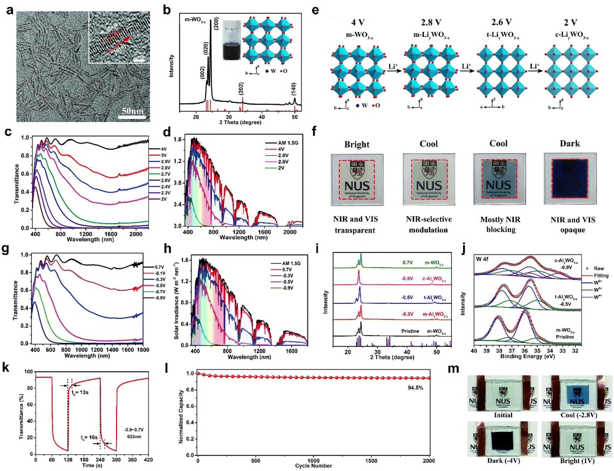 | ||
| Fig. 7 (a) TEM image, (b) XRD pattern of m-WO3−x NWs. (c) Optical transmittance spectra, (d) solar irradiance spectra of the m-WO3−x NW film. (e) Crystal structures and (f) corresponding photos of m-WO3−x NW films at 4 V, 2.8 V, 2.6 V., and 2 V (vs. Li+/Li), respectively. (a–f) Adapted with permission from ref. 44. Copyright 2018, Royal Society of Chemistry. (g) Transmittance spectra, (h) solar irradiance spectra, (i) XRD patterns, (j) W 4f XPS spectra, (k) switching speed, (l) cycling stability of m-WO3−x NW films in Al3+-based electrolyte. (m) Digital phots of the Al3+-based device. (g–m) Adapted with permission from ref. 61. Copyright 2018, Royal Society of Chemistry. | ||
As shown in Fig. 8a–e, Cai et al.70 recently prepared a type of porous WO3 film with nanowires/nanoparticles core/shell architecture as a promising candidate for smart windows with a dual-band electrochromic feature. The results indicated that the dual-band electrochromic performance was credited to the progressive electrochemical reduction procedure, in which the capacitive charging process gave rise to NIR regulation and the following ion intercalation contributed to VIS light modulation. Inspired by pine needles, Zhang et al.71 synthesized a unique pine-needle-like (PNL) W18O49/TiO2 heterostructure (Fig. 8f), which was constructed with W18O49 nanowires (as branches) and TiO2 nanofibers (as backbones). The PNL-W18O49/TiO2 heterostructures exhibited superior dual-band EC performance in both VIS and NIR bands (Fig. 8h–k), which can block up to 81.4% of the VIS light at 633 nm and they also showed extremely short bleaching/coloring time (0.9/1.2 s) and excellent stability (85% of capacity retention after 20000 cycles).
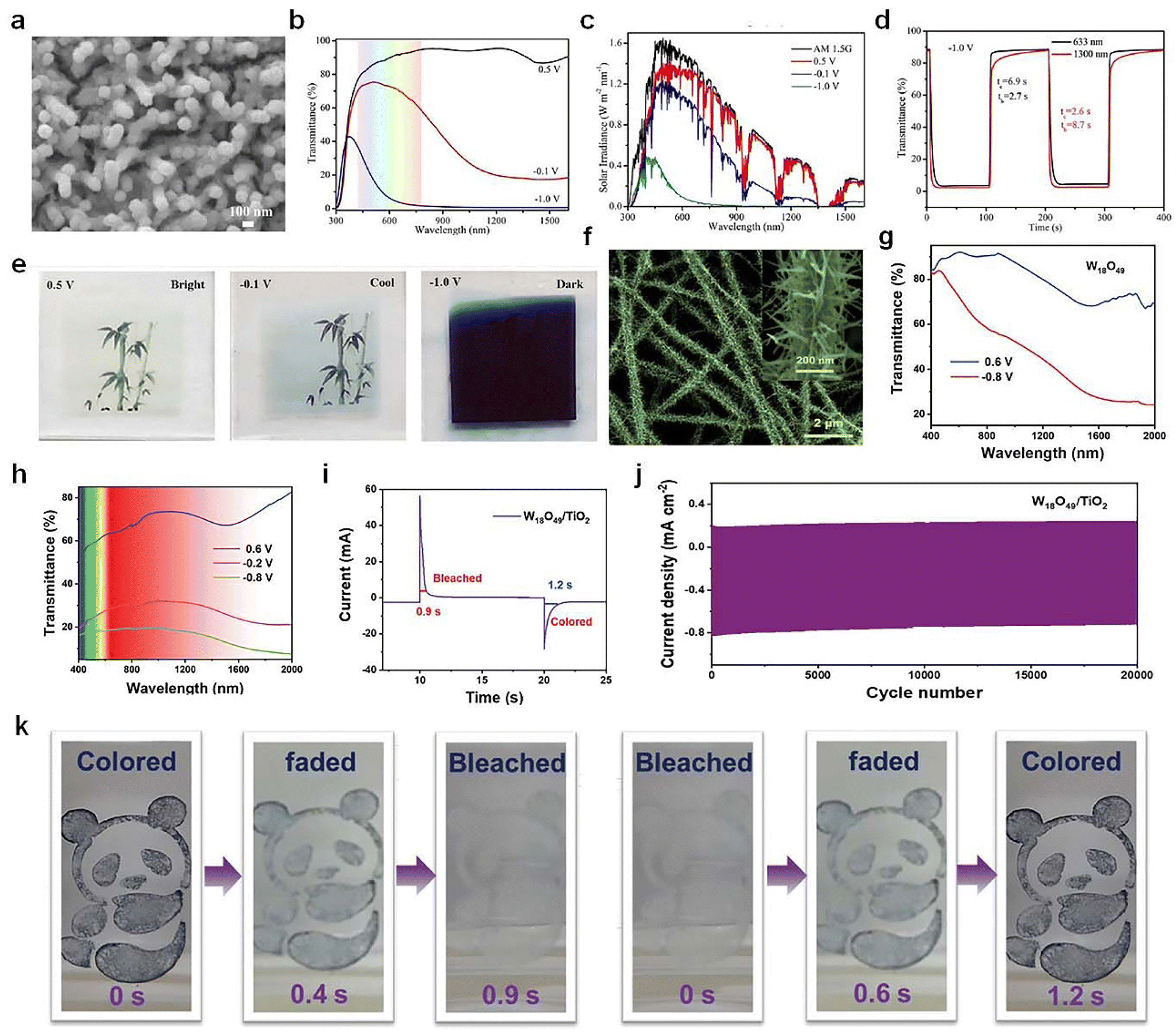 | ||
| Fig. 8 (a) SEM image, (b) optical transmittance spectra, (c) solar irradiance spectra, (d) switching speed, and (e) digital photos of the WO3 NWs/NPs film. (a–e) Adapted with permission from ref. 70. Copyright 2023, American Chemical Society. (f) SEM image of the W18O49/TiO2 heterostructures. Transmittance spectra of (g) W18O49 nanowires and (h) PNL-W18O49/TiO2 heterostructures. (i) Switching speed, (j) cycling stability, and (k) optical images of W18O49/TiO2 heterostructures. (f–k) Adapted with permission from ref. 71. Copyright 2022, Wiley-VCH. | ||
Zn is abundant, safe, easily processed in aqueous electrolytes and provides two electrons during redox reactions, which is conductive for triggering electrochromism via Zn2+ intercalation. Li et al.72 recently reported a Zn-based electrochromic battery utilizing the Ti-substituted tungsten molybdenum oxide (MTWO, Fig. 9a) nanowires. Ti-doping clearly enhanced the intercalation of Zn2+, yielding improved capacity and electrochromic performance (Fig. 9c–d). The Zn-based electrochromic batteries (Fig. 9e and f) exhibited an areal capacity of 260 mA h m−2 and high optical contrast (76%). Gao et al.73 reported an electro-chromic-chemical device (MED) in large area made of W17O47 nanowires, where Zn2+ ion intercalation took place in the oxygen-vacancy monoclinic WO3 with WO polyhedral. The large-area MEDs assembled with W17O47/NaWO3 NW electrodes (Fig. 9g) exhibited excellent energy-saving and energy-storage properties. The W17O47/NaWO3 electrode materials exhibited excellent high optical modulation and fast switching speed (Fig. 9h and i). Furthermore, a large area Zn-based MED assembled with the W17O47/NaWO3 NW electrode (30.5 cm × 26 cm, Fig. 9j) was demonstrated in a model window, which also showed high electrochromic performance and good stability, suggesting the great potential of Zn-based MED based on W17O47/NaWO3 NWs.
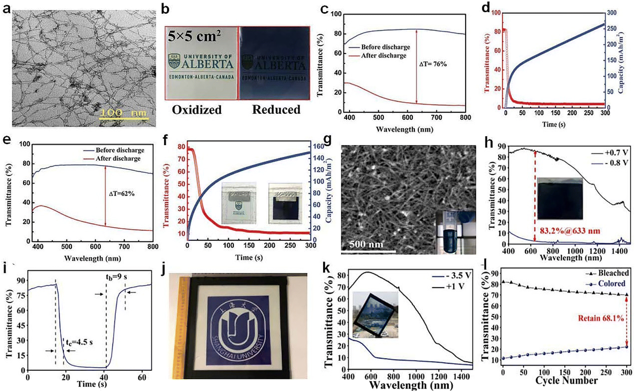 | ||
| Fig. 9 (a) TEM image of the MTWO. (b) Photographs, (c) transmittance spectra, and (d) self-coloring (discharge) process of a MTWO cathode. (e) Transmittance spectra, (f) self-coloring process of the Zn-based EC device. (a–f) Adapted with permission from ref. 72. Copyright 2019, Wiley-VCH. (g) SEM image, (h) transmittance spectra, (i) switching speed of W17O47/NaWO3 NW electrode. (j) Photograph, (k) transmittance spectra, and (l) cycling stability of the prototype MED. (g–l) Adapted with permission from ref. 73. Copyright 2021, Elsevier. | ||
Co-assembly of various nanowires represents a promising technology for fabricating next-generation multifunctional electronics. For example, Yu et al.74 demonstrated a novel multicolor electrochromic device by co-assembling W18O49 and V2O5 NWs using solution-based Langmuir–Blodgett (LB) technique (Fig. 10a and b). The transparent W18O49/V2O5 NW film showed a dynamic color change (orange, green, and gray) by controlling the applied voltages (Fig. 10c and d). Both the transmittance and color of the device can be easily controlled by manipulating the layers of co-assembled NWs and the ratios between the two NWs. Recently, Yu et al.75 used the co-assembly strategy to fabricated the selective light absorption electrochromic (SLE) smart window by integrating W18O49 NWs and Au nanorods (Fig. 10e). The prepared W18O49/Au films exhibited enhanced EC performance (Fig. 10f–h), especially for NIR-selective modulation due to the strong LSPR of Au, which significantly improved the cooling efficiency of EC windows.
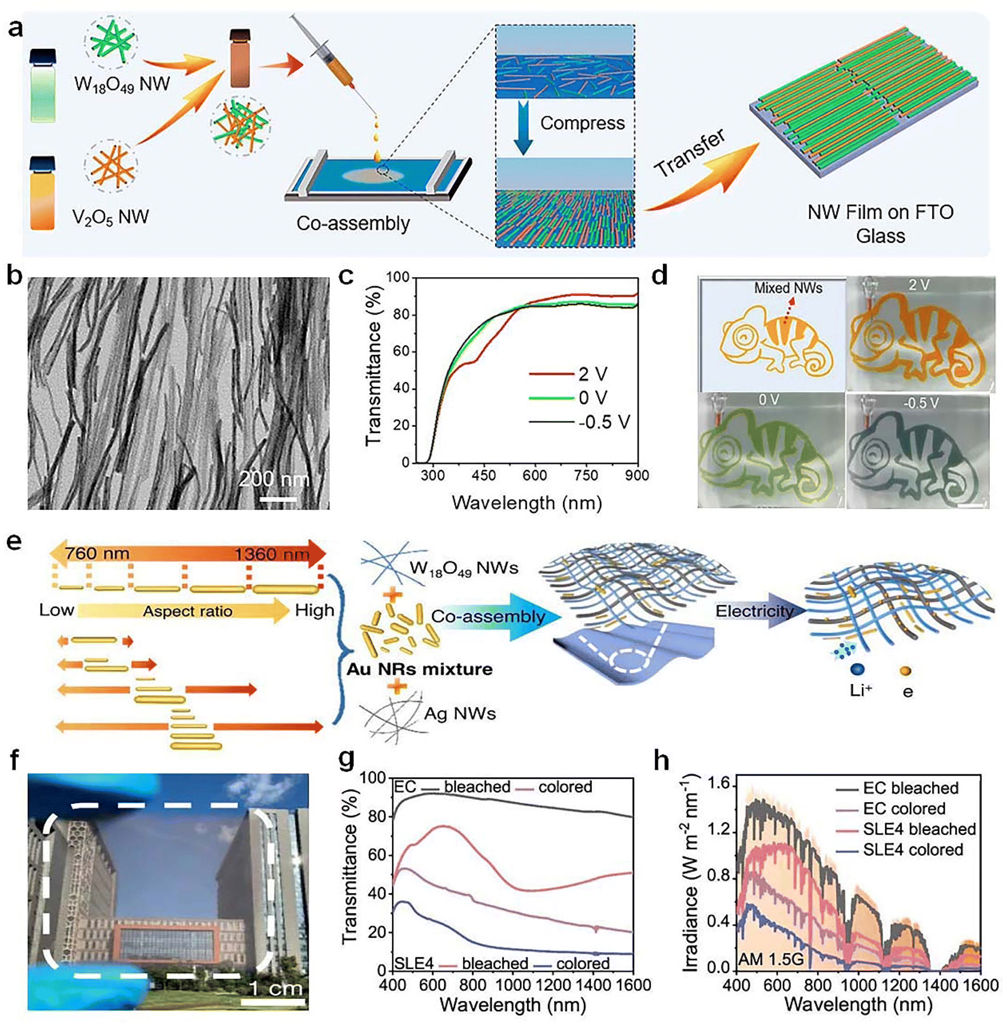 | ||
| Fig. 10 (a) Schematic illustration for co-assembling W18O49 and V2O5 NWs based on LB technique. (b) TEM image, (c) optical transmittance spectra, and (d) digital photos of the as-prepared W18O49/V2O5 NW film. (a–d) Adapted with permission from ref. 74. Copyright 2021, American Chemical Society. (e) Schematic illustration on the co-assembly of W18O49 nanowires and Au nanorods. (f) Digital photo, (g) optical transmittance spectra, and (h) solar spectral irradiance of the prepared W18O49/Au films. (e–h) Adapted with permission from ref. 75. Copyright 2023, Springer Nature. | ||
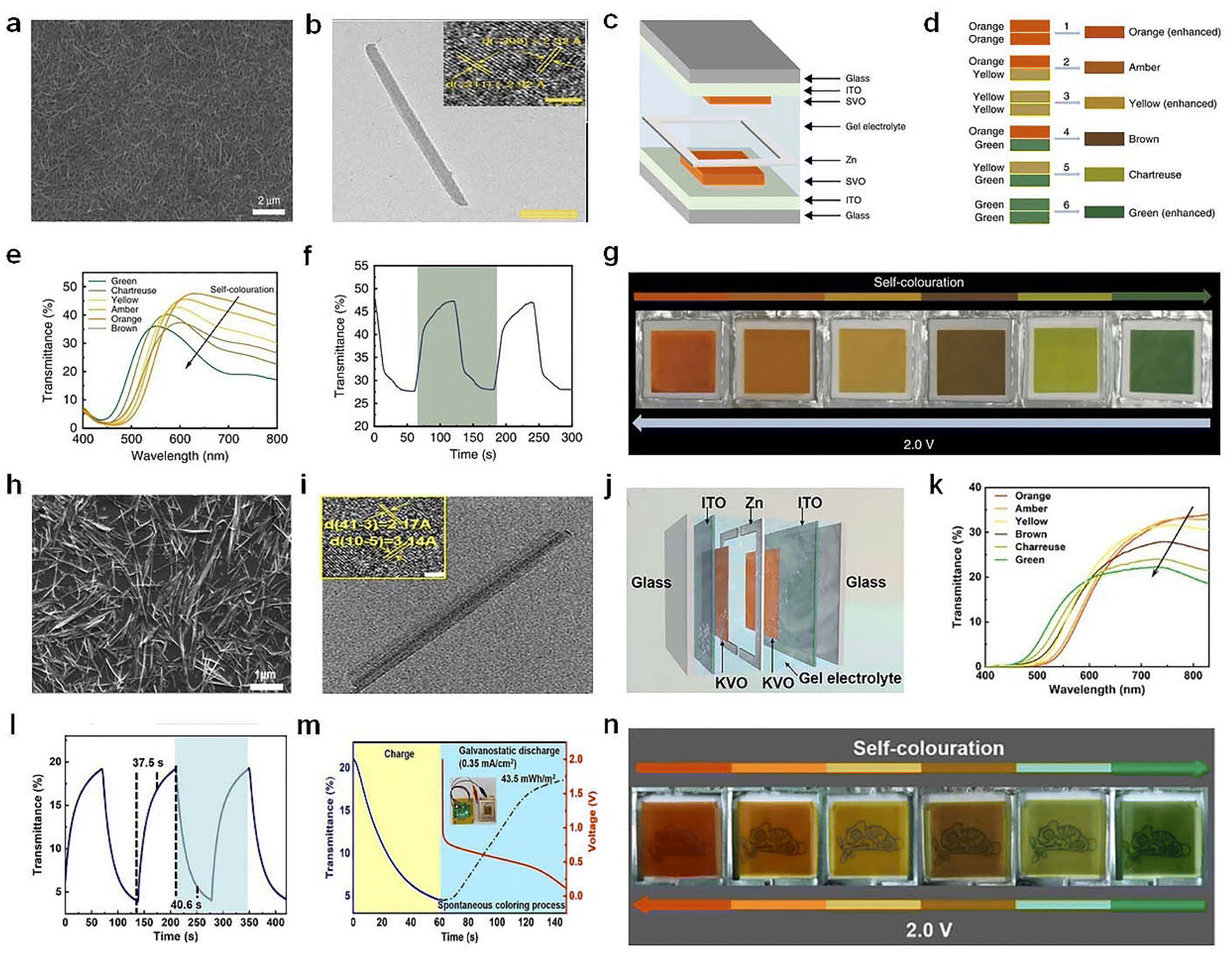 | ||
| Fig. 11 (a) SEM and (b) TEM images of the SVO nanorods. (c) Schematic illustration of Zn–SVO EC display and (d) the color overlap effect. (e) Transmittance spectra, (f) switching time, (g) digital photos of the Zn–SVO device under different voltages. (a–g) Adapted with permission from ref. 76. Copyright 2020, Springer Nature. (h) SEM and (i) TEM images of the KVO nanorods. (j) Schematic diagram, (k) optical transmittance spectra, (l) switching speed, (m) energy-recycling performance, and (n) digital photos of the Zn–KVO EC display. (h–n) Adapted with permission from ref. 77. Copyright 2023, Wiley-VCH. | ||
2.3. Two-dimensional (2D) inorganic EC materials
Two-dimensional (2D) materials are sheet-like nanomaterials composed of single or multiple layers of atoms or molecules. Its transverse size can reach tens of microns or even larger. 2D materials exhibit unusual physicochemical properties due to their unique internal structure.78 The surface atoms of 2D materials are almost completely exposed and the utilization rate of the atoms is greatly improved. By stacking layers and mixing elements, it is easier to adjust the band structure and performance. Atomic thickness brings excellent flatness and structural stability, and ultrathin thickness gives excellent bending properties to 2D materials, making them the first choice for flexible EC devices.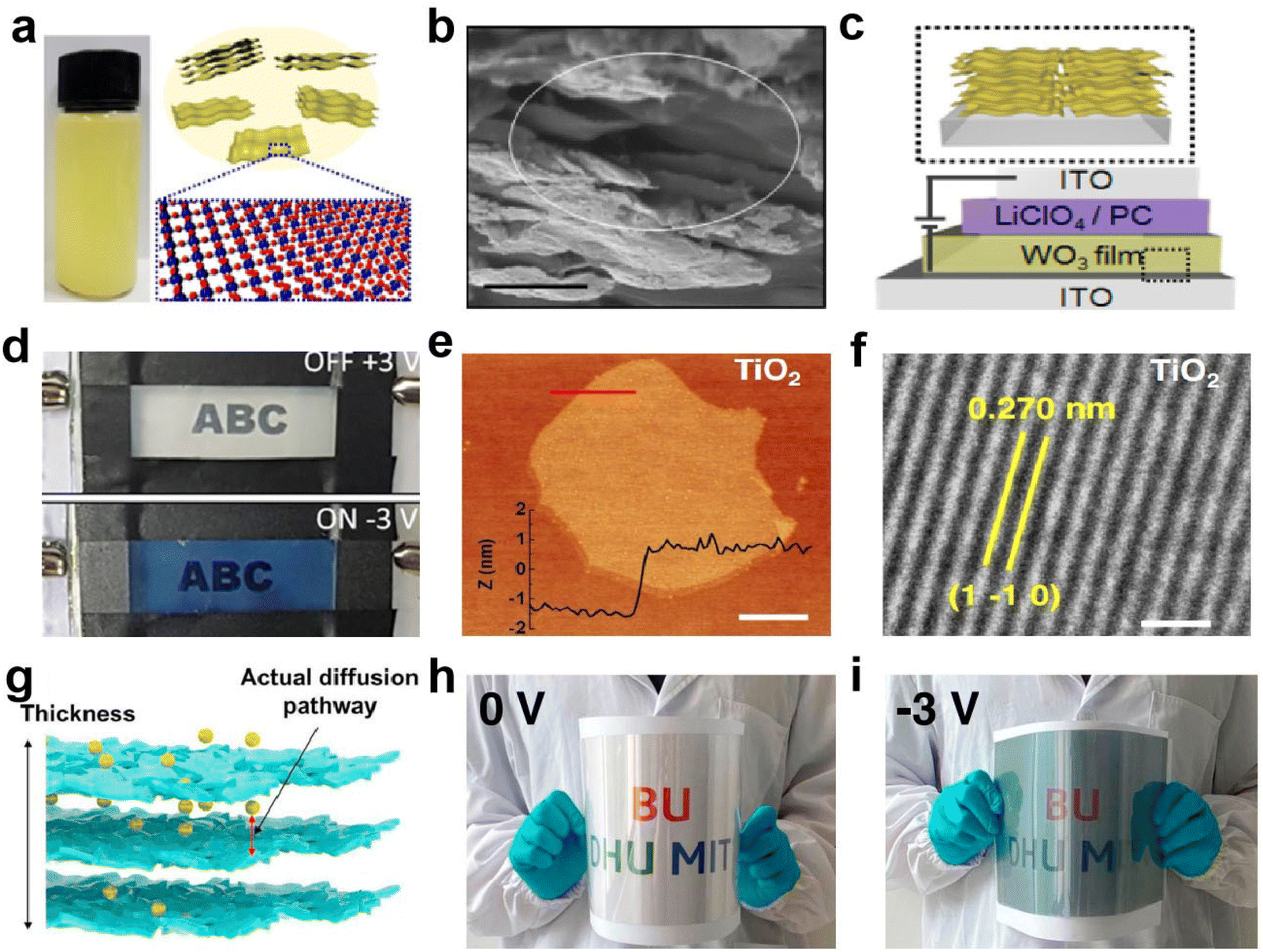 | ||
| Fig. 12 (a) Schematic diagram and (b) SEM image of 2D WO3 nanosheets. (c) Schematic diagram and (d) digital photos of the EC device based on WO3 nanosheets. (a–d) Adapted with permission from ref. 79. Copyright 2018, American Chemical Society. (e) AFM and (f) HRTEM images of TiO2 sheet. (g) Schematic diagram of self-assembled 2D TiO2 films. (h and i) The digital photos of the large-area device in the bent state. (e–i) Adapted with permission from ref. 80. Copyright 2021, Springer Nature. | ||
 | ||
| Fig. 13 (a) Structure diagram, (b and c) principal diagram of graphene-based device. (d) Spectra of the thermal radiation from the graphene-based device at voltages. (e and f) Thermal camera images of device at 0 V and 3 V. (a–f) Adapted with permission from ref. 18. Copyright 2018, American Chemical Society. (g) Schematic diagram of the textile device with various laminated layers. (h) Infrared reflectance spectra of the textile at different voltages. (g and h) Adapted with permission from ref. 19. Copyright 2020, American Chemical Society. | ||
000 cycles (Fig. 14f–h). They also revealed the actuation mechanism, which can be attributed to the expansion and contraction of the MXene layer spacing.
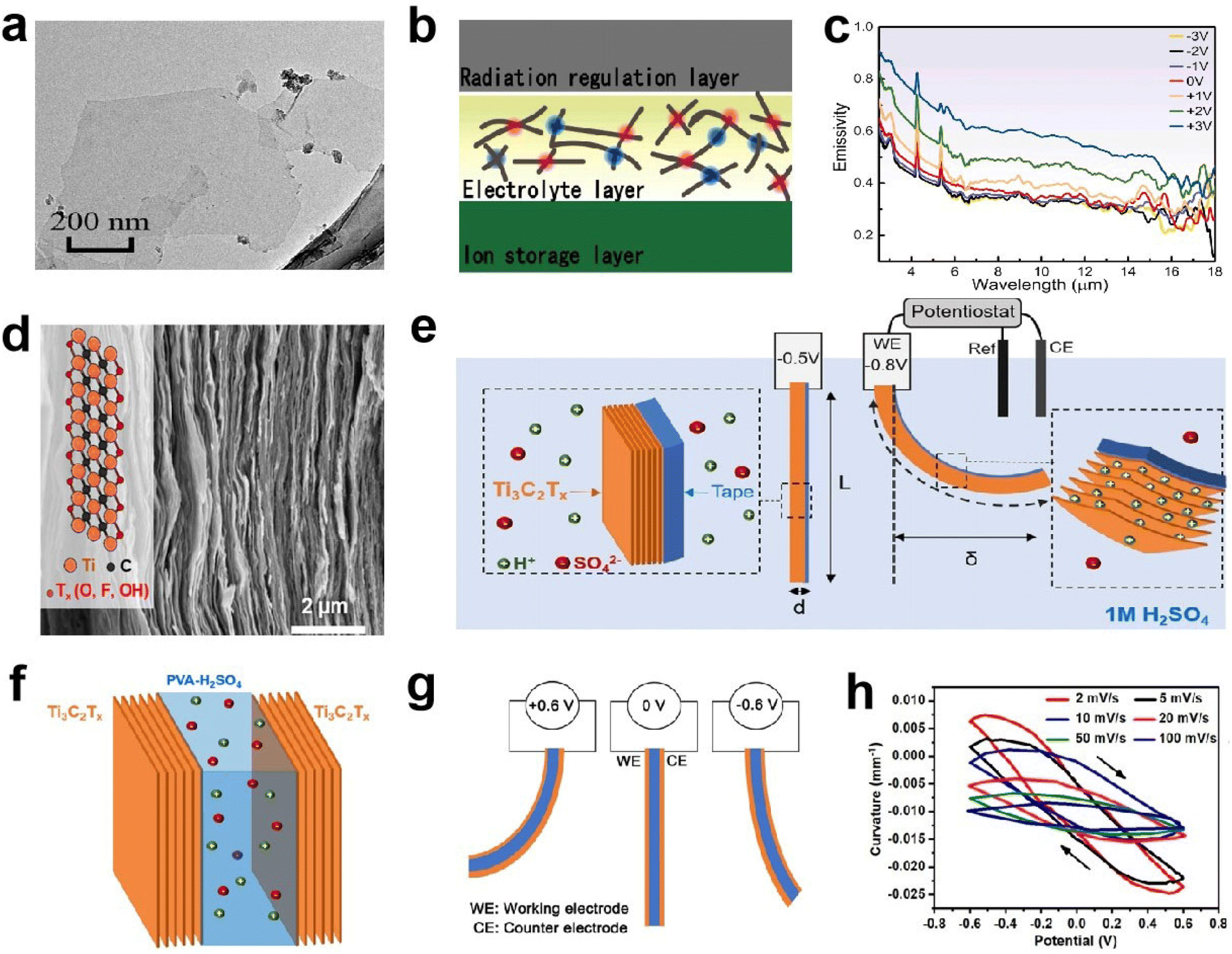 | ||
| Fig. 14 (a) HRTEM image of MXene nanosheets. (b) Structure and (c) emissivity of the MXene-based EC device. (a–c) Adapted with permission from ref. 83. Copyright 2022, Elsevier. (d) Cross-sectional SEM image of a Ti3C2Tx electrode. (e) Schematic representation of the EC film. (f and g) The configuration and (h) curvature of the EC actuator. (d–h) Adapted with permission from ref. 84. Copyright 2019, American Chemical Society. | ||
3. Summary and prospects
With the rapid development of EC and nanoscience fields, significant progress has been made on advanced inorganic EC nanomaterials and devices for light and thermal management in the past few years. In this review, we systematically summarize and discuss the recent advances in advanced inorganic EC nanomaterials, mainly focusing on low dimensional transition metal oxides (e.g., WO3, TiO2, NiO, Nb18W16O93, and V2O5), graphene, and MXenes (Table 1). Taking advantages of the short ion diffusion distance, fast ion diffusion speed, and high surface area, nanomaterials not only notably improve the switching speed of EC process but also enhance the optical modulation and cycle stability of EC devices. Consequently, advanced inorganic EC materials have shown great potential applications in energy-saving smart windows, biostable displays, and adaptive thermal management.| Material | ΔT633nm | t c/tb (s) | CE (cm2 C−1) | Cycle stability | Ref. |
|---|---|---|---|---|---|
| NbOx-WO3−x NC film | ∼80% | 600/100 | N/A | 2000 cycles (5.7% capacity loss) | 36 |
| Ti-WO3 NC film | 84.9% | 3.3/25 | 114.9 | 1000 cycles (11% optical loss) | 48 |
| WO3 QD film | Li+: 97.8% | Li+: 4.5/4 | Li+: 76.8 | Li+: 10000 cycles (10% optical loss) |
50 |
| Al3+: 94.1% | Al3+: 13.5/10 | Al3+: 82.9 | Al3+: 20000 cycles |
||
| WO3−x NC device | 76% | 4.5/3.7 | 97.7 | 1000 cycles (30% capacity loss) | 55 |
| Ta-TiO2 NC film | ∼90% | 66.8/6.9 (550 nm) | 33.2 (550 nm) | 2000 cycles (14.8% capacity loss) | 57 |
| W-TiO2 NC device | 77% | 7.9/5.8 | 37.3 (550 nm) | 1000 cycles (8.9% capacity loss) | 42 |
| TiO2−x NC film | 95.5% | 15.5/3.4 | 38.2 | 2000 cycles (4.4% capacity loss) | 64 |
| NiO NC film | ∼75% | N/A | 75.5 (550 nm) | N/A | 67 |
| Nb18W16O93 NC film | 96.2% | 7/29 | 72.4 | 3500 cycles (28% optical loss) | 68 |
| m-WO3−x NW film | Li+: 91.7% | Li+: 21/85 | Li+: 101.7 | Li+: 1000 cycles (20% capacity loss) | 44 |
| Al3+: 93.2% | Al3+: 16/13 | Al3+: 121 | Al3+: 2000 cycles (5.5% capacity loss) | 61 | |
| WO3 NWs/NPs film | 87.1% | 6.9/2.7 | 79.2 | 1000 cycles (32.3% optical loss) | 70 |
| MTWO NW film | 76% | Self-coloration time: 14 | N/A | N/A | 72 |
| W17O49 NW film | 83.2% | 4.5/9 | N/A | 4000 cycles (25.7% optical loss) | 73 |
| W18O49 NW/Au film | ∼50% | 4.5/4.0 | 48.46 | N/A | 75 |
| WO3 Nanosheets device | ∼51% | 10.74/6.97 (700 nm) | N/A | 1000 cycles (6% capacity loss) | 79 |
| TiO2/Ti3C2Tx Nanosheets film | ∼48% | 1.71/0.3 (550 nm) | 243 | 1000 cycles (8% optical loss) | 80 |
| Graphene device | 43% (10 μm) | <1/<1 | N/A | 500 cycles | 18 |
Although significant achievements have been made, there are still some challenges in inorganic EC nanomaterials for practical applications.
(1) Mass preparation of inorganic EC nanomaterials: whether the inorganic EC nanomaterials with high quality and uniformity can be prepared in large quantities is a crucial factor for the future practical applications. Currently, a lot of synthetic methods such as solvothermal, sol–gel, colloidal, electrodeposition, and electrospinning have been developed for preparing high-quality nanomaterials. However, the mass of prepared nanomaterials is usually at the gram level, which is definitely not beneficial to practical application. For large-scale commercialization, mass preparation (at the kilogram level) of high-quality inorganic EC nanomaterials with a low-cost and facile process is essential.
(2) Low-cost and large-area film-forming technology: the high-quality film-forming technology with low-cost and large-area is another issue in the development of nanomaterial-based EC devices. The traditional EC film-forming technologies such as magnetron sputtering, vacuum evaporation, and spin-coating, which is either high-cost or small-area, are not suitable for next-generation EC devices with large-area and low-cost. Actually, a few other film-forming technologies such as automatic blade coating and roll-to-roll coating have been widely used in some other research fields (e.g., batteries). These technologies might be able to address the current issue of electrochromic film preparation. However, the thickness of electrochromic film is only a few hundreds of nanometers, having a large difference with the thickness of battery electrodes (> dozens of micrometers). Consequently, how to acquire a high-uniform and high-quality electrochromic film using automatic blade coating or roll-to-roll coating is still a challenge, needing a long way to go for optimization and commercial production.
(3) Side reactions resulted from nanomaterials: although the high surface area of nanomaterials can increase the ion storage sites and contact area between the electrode and electrolyte, it can also cause some undesired side reactions such as catalyzing the decomposition of electrolyte due to the high reactivity. The decomposition of electrolyte will produce some gases such as carbon dioxide, causing the bubble issue of EC devices. Therefore, how to inhibit the side reactions is essential for the nanomaterial-based EC device. Besides the nanomaterials, the occurrence of side reactions is also related to the solid–liquid interface, electrolyte composition, electrode potential, and device structure. Consequently, interface designing, electrolyte optimization, reducing operating voltage, device structure design, and optimization are possible approaches to address the issue of side reaction.
Fortunately, more and more scientific and industrial researchers have started to conduct research works on electrochromism and try their best to address the problems of EC materials and devices. We suppose that significant breakthroughs will be achieved on nanomaterial-based EC devices in the near future. We also believe that the electrochromism technology will be widely used in our life and significantly improve the quality of our life in the future.
Conflicts of interest
The authors declare no conflict of interest.Acknowledgements
This work was supported by the National Natural Science Foundation of China (62105148), Innovation and Entrepreneurship Talent Project of Jiangsu (JSSCBS20210191), China Postdoctoral Science Foundation (2022TQ0148 and 2023M731651), and High-Level Foreign Expert Project (G2022181026L).References
- C. Gu, A. B. Jia, Y. M. Zhang and S. X. Zhang, Chem. Rev., 2022, 122, 14679–14721 CrossRef CAS PubMed.
- F. Zhao, B. Wang, W. Zhang, S. Cao, L. Liu, A. Y. Elezzabi, H. Li and W. W. Yu, Mater. Today, 2023, 66, 431–447 CrossRef.
- Z. Shao, A. Huang, C. Ming, J. Bell, P. Yu, Y.-Y. Sun, L. Jin, L. Ma, H. Luo, P. Jin and X. Cao, Nat. Electron., 2022, 5, 45–52 CrossRef CAS.
- Y. Ding, M. Wang, Z. Mei and X. Diao, ACS Appl. Mater. Interfaces, 2022, 14, 48833–48843 CrossRef CAS PubMed.
- Y. Su, Y. Wang, Z. Lu, M. Tian, F. Wang, M. Wang, X. Diao and X. Zhong, Chem. Eng. J., 2023, 456, 141075 CrossRef CAS.
- Z. Zhou, Z. Chen, D. Ma and J. Wang, Sol. Energy Mater. Sol. Cells, 2023, 253, 112226 CrossRef CAS.
- W. Zhao, J. Wang, B. Tam, H. Zhang, F. Li, A. Du and W. Cheng, Adv. Opt. Mater., 2023, 11, 2202774 CrossRef CAS.
- S. Zhang, Y. Peng, J. Zhao, Z. Fan, B. Ding, J. Y. Lee, X. Zhang and Y. Xuan, Adv. Opt. Mater., 2022, 11, 2202115 CrossRef.
- S. Zhang, S. Cao, T. Zhang, Q. Yao, H. Lin, A. Fisher and J. Y. Lee, Small Methods, 2019, 4, 1900545 CrossRef.
- J. Chen, A. W. M. Tan, A. L.-S. Eh and P. S. Lee, Adv. Energy Sustainability Res., 2021, 3, 2100172 CrossRef.
- Y. Wang, S. Wang, X. Wang, W. Zhang, W. Zheng, Y.-M. Zhang and S. X.-A. Zhang, Nat. Mater., 2019, 18, 1335–1342 CrossRef CAS PubMed.
- J. Chen, Y. Li, T. Zhang, X. Zha, X. Tang, X. Mu, P. Sun, G. Song, S. Cong, Q. Chen and Z. Zhao, Laser Photonics Rev., 2022, 16, 2200303 CrossRef CAS.
- Y. Li, P. Sun, J. Chen, X. Zha, X. Tang, Z. Chen, Y. Zhang, S. Cong, F. Geng and Z. Zhao, Adv. Mater., 2023, 35, 2300116 CrossRef CAS PubMed.
- H. Wei, J. Gu, F. Ren, L. Zhang, G. Xu, B. Wang, S. Song, J. Zhao, S. Dou and Y. Li, Small, 2021, 17, e2100446 CrossRef PubMed.
- W. Sun, X. Zhang, H. Zhang, Z. Ren, M. Chen, Y. Xiao, Z. Li, J. Deng, D. Yan, L. Zhang and Y. Li, Laser Photonics Rev., 2023, 17, 2300476 CrossRef CAS.
- H. Gong, W. Li, G. Fu, Q. Zhang, J. Liu, Y. Jin and H. Wang, J. Mater. Chem. A, 2022, 10, 6269–6290 RSC.
- L. Zhang, T. Hao, S. Song, B. Wang, D. Liu, Z. Ren, W. Liu, Y. Zhang, G. Xu, X. Yan, Y. Lu and Y. Li, Chem. Eng. J., 2023, 475, 145927 CrossRef CAS.
- O. Salihoglu, H. B. Uzlu, O. Yakar, S. Aas, O. Balci, N. Kakenov, S. Balci, S. Olcum, S. Suzer and C. Kocabas, Nano Lett., 2018, 18, 4541–4548 CrossRef CAS PubMed.
- M. S. Ergoktas, G. Bakan, P. Steiner, C. Bartlam, Y. Malevich, E. Ozden-Yenigun, G. He, N. Karim, P. Cataldi, M. A. Bissett, I. A. Kinloch, K. S. Novoselov and C. Kocabas, Nano Lett., 2020, 20, 5346–5352 CrossRef CAS PubMed.
- J. Guo, H. Jia, Z. Shao, P. Jin and X. Cao, Acc. Mater. Res., 2023, 4, 438–447 CrossRef CAS.
- J. Li, Y. Zhuang, J. Chen, B. Li, L. Wang, S. Liu and Q. Zhao, Energy Chem., 2021, 3, 100060 CrossRef CAS.
- Y. Huang, B. Wang, F. Chen, Y. Han, W. Zhang, X. Wu, R. Li, Q. Jiang, X. Jia and R. Zhang, Adv. Opt. Mater., 2021, 2101783 Search PubMed.
- S. Kandpal, T. Ghosh, C. Rani, A. Chaudhary, J. Park, P. S. Lee and R. Kumar, ACS Energy Lett., 2023, 8, 1870–1886 CrossRef CAS.
- Q. Zhao, Z. Pan, B. Liu, C. Bao, X. Liu, J. Sun, S. Xie, Q. Wang, J. Wang and Y. Gao, Nano-Micro Lett., 2023, 15, 87 CrossRef PubMed.
- X. Wu, Q. Fan, Z. Bai, Q. Zhang, W. Jiang, Y. Li, C. Hou, K. Li and H. Wang, Small, 2023, 19, 2301742 CrossRef CAS PubMed.
- D. Zhang, J. Wang, Z. Tong, H. Ji and H. Y. Qu, Adv. Funct. Mater., 2021, 31, 2106577 CrossRef CAS.
- X. Lv, J. Li, L. Xu, X. Zhu, A. Tameev, A. Nekrasov, G. Kim, H. Xu and C. Zhang, ACS Appl. Mater. Interfaces, 2021, 13, 41826–41835 CrossRef CAS PubMed.
- M. Shao, D. Ji, Z. Xu, J. Dong, X. Lv, M. Ouyang, Y. Lv, D. S. Wright and C. Zhang, J. Power Sources, 2023, 581, 233490 CrossRef CAS.
- G. Yang, Y. M. Zhang, Y. Cai, B. Yang, C. Gu and S. X. Zhang, Chem. Soc. Rev., 2020, 49, 8687–8720 RSC.
- B. Wang, W. Zhang, F. Zhao, W. W. Yu, A. Y. Elezzabi, L. Liu and H. Li, Nano Mater. Sci., 2022, 5, 369–391 CrossRef.
- W. Zhang, H. Li, E. Hopmann and A. Y. Elezzabi, Nanophotonics, 2020, 10, 825–850 CrossRef.
- S. Zhang, Y. Li, T. Zhang, S. Cao, Q. Yao, H. Lin, H. Ye, A. Fisher and J. Y. Lee, ACS Appl. Mater. Interfaces, 2019, 11, 48062–48070 CrossRef CAS PubMed.
- S. Huang, R. Zhang, P. Shao, Y. Zhang and R. T. Wen, Adv. Opt. Mater., 2022, 10, 2200903 CrossRef CAS.
- J. Wang, W. Zhao, B. Tam, H. Zhang, Y. Zhou, L. Yong and W. Cheng, Chem. Eng. J., 2023, 452, 139655 CrossRef CAS.
- W. Zhao, J. Wang, B. Tam, P. Pei, F. Li, A. Xie and W. Cheng, ACS Appl. Mater. Interfaces, 2022, 14, 30021–30028 CrossRef CAS PubMed.
- J. Kim, G. K. Ong, Y. Wang, G. LeBlanc, T. E. Williams, T. M. Mattox, B. A. Helms and D. J. Milliron, Nano Lett., 2015, 15, 5574–5579 CrossRef CAS PubMed.
- B. Huang, J. Song, J. Zhong, H. Wang, X. Zheng, J. Jia, S. Yun, D. You, H. Kimura and L. Kang, Chem. Eng. J., 2022, 449, 137850 CrossRef CAS.
- H. Li, W. Zhang and A. Y. Elezzabi, Adv. Mater., 2020, 32, 2003574 CrossRef CAS PubMed.
- Q. Meng, S. Cao, J. Guo, Q. Wang, K. Wang, T. Yang, R. Zeng, J. Zhao and B. Zou, J. Energy Chem., 2022, 77, 137–143 CrossRef.
- Y. Yao, Q. Zhao, W. Wei, Z. Chen, Y. Zhu, P. Zhang, Z. Zhang and Y. Gao, Nano Energy, 2020, 68, 104350 CrossRef CAS.
- S. Cao, S. Zhang, T. Zhang, Q. Yao and J. Y. Lee, Joule, 2019, 3, 1152–1162 CrossRef CAS.
- Y. Liang, S. Cao, Q. Wei, R. Zeng, J. Zhao, H. Li, W. W. Yu and B. Zou, Nano-Micro Lett., 2021, 13, 196 CrossRef CAS PubMed.
- S. Zhang, S. Cao, T. Zhang and J. Y. Lee, Adv. Mater., 2020, 32, 2004686 CrossRef CAS PubMed.
- S. Zhang, S. Cao, T. Zhang, Q. Yao, A. Fisher and J. Y. Lee, Mater. Horiz., 2018, 5, 291–297 RSC.
- S. Zhang, S. Cao, T. Zhang, A. Fisher and J. Y. Lee, Energy Environ. Sci., 2018, 11, 2884–2892 RSC.
- H. Li, L. McRae, C. J. Firby and A. Y. Elezzabi, Adv. Mater., 2019, 31, 1807065 CrossRef PubMed.
- Q. Zhao, J. Wang, X. Ai, Z. Pan, F. Xu, J. Wang and Y. Gao, Nano Energy, 2021, 89, 106356 CrossRef CAS.
- Q. Meng, S. Cao, J. Guo, Q. Wang, K. Wang, T. Yang, R. Zeng, J. Zhao and B. Zou, J. Energy Chem., 2023, 77, 137–143 CrossRef CAS.
- S. Cong, Y. Tian, Q. Li, Z. Zhao and F. Geng, Adv. Mater., 2014, 26, 4260–4267 CrossRef CAS PubMed.
- Y. Yao, Q. Zhao, W. Wei, Z. Chen, Y. Zhu, P. Zhang, Z. Zhang and Y. Gao, Nano Energy, 2020, 68, 104350 CrossRef CAS.
- D. McManus, S. Vranic, F. Withers, V. Sanchez-Romaguera, M. Macucci, H. Yang, R. Sorrentino, K. Parvez, S. K. Son, G. Iannaccone, K. Kostarelos, G. Fiori and C. Casiraghi, Nat. Nanotechnol., 2017, 12, 343–350 CrossRef CAS PubMed.
- G. Li, Z. Meng, J. Qian, C.-L. Ho, S. P. Lau, W.-Y. Wong and F. Yan, Mater. Today Energy, 2019, 12, 155–160 CrossRef.
- P. Yang, L. Zhang, D. J. Kang, R. Strahl and T. Kraus, Adv. Opt. Mater., 2019, 8, 1901429 CrossRef.
- G. Hu, J. Kang, L. W. T. Ng, X. Zhu, R. C. T. Howe, C. G. Jones, M. C. Hersam and T. Hasan, Chem. Soc. Rev., 2018, 47, 3265–3300 RSC.
- L. Zhang, D. Chao, P. Yang, L. Weber, J. Li, T. Kraus and H. J. Fan, Adv. Energy Mater., 2020, 10, 2000142 CrossRef CAS.
- M. Barawi, G. Veramonti, M. Epifani, R. Giannuzzi, T. Sibillano, C. Giannini, A. Rougier and M. Manca, J. Mater. Chem. A, 2018, 6, 10201–10205 RSC.
- S. Cao, S. Zhang, T. Zhang and J. Y. Lee, Chem. Mater., 2018, 30, 4838–4846 CrossRef CAS.
- R. Giannuzzi, T. Prontera, D. M. Tobaldi, M. Pugliese, L. De Marco, S. Carallo, G. Gigli, R. C. Pullar and V. Maiorano, Nanotechnology, 2021, 32, 045703 CrossRef CAS PubMed.
- L. De Trizio, R. Buonsanti, A. M. Schimpf, A. Llordes, D. R. Gamelin, R. Simonutti and D. J. Milliron, Chem. Mater., 2013, 25, 3383–3390 CrossRef CAS.
- C. J. Dahlman, Y. Tan, M. A. Marcus and D. J. Milliron, J. Am. Chem. Soc., 2015, 137, 9160–9166 CrossRef CAS PubMed.
- S. Cao, S. Zhang, T. Zhang, A. Fisher and J. Y. Lee, J. Mater. Chem. C, 2018, 6, 4007–4014 RSC.
- A. Agrawal, S. H. Cho, O. Zandi, S. Ghosh, R. W. Johns and D. J. Milliron, Chem. Rev., 2018, 118, 3121–3207 CrossRef CAS PubMed.
- T. R. Gordon, M. Cargnello, T. Paik, F. Mangolini, R. T. Weber, P. Fornasiero and C. B. Murray, J. Am. Chem. Soc., 2012, 134, 6751–6761 CrossRef CAS PubMed.
- S. Zhang, S. Cao, T. Zhang and J. Y. Lee, Adv. Mater., 2020, 32, 2004686 CrossRef CAS PubMed.
- P. Lei, J. Wang, P. Zhang, S. Liu, S. Zhang, Y. Gao, J. Tu and G. Cai, J. Mater. Chem. C, 2021, 9, 14378–14387 RSC.
- X. Ju, F. Yang, X. Zhu and X. Jia, ACS Sustainable Chem. Eng., 2020, 8, 12222–12229 CrossRef CAS.
- J. Wang, R. Zhu, Y. Gao, Y. Jia and G. Cai, J. Phys. Chem. Lett., 2023, 14, 2284–2291 CrossRef CAS PubMed.
- K. J. Griffith, K. M. Wiaderek, G. Cibin, L. E. Marbella and C. P. Grey, Nature, 2018, 559, 556–563 CrossRef CAS PubMed.
- R. Ren, S. Liu, Y. Gao, P. Lei, J. Wang, X. Tong, P. Zhang, Z. Wang and G. Cai, ACS Energy Lett., 2023, 8, 2300–2307 CrossRef CAS.
- H. Liu, Y. Zhang, P. Lei, J. Feng, S. Jia, J. Huang, C. Hu, C. Bian and G. Cai, ACS Appl. Mater. Interfaces, 2023, 15, 23412–23420 CrossRef CAS PubMed.
- Y. Huang, B. Wang, X. Bai, Y. Han, W. Zhang, C. Zhou, H. Meng, F. Chen, X. Wu, Q. Jiang, R. Li, S. Zhang, X. Jia and R. Zhang, Adv. Opt. Mater., 2022, 10, 2102399 CrossRef CAS.
- H. Li, L. McRae, C. J. Firby and A. Y. Elezzabi, Adv. Mater., 2019, 31, 1807065 CrossRef PubMed.
- Q. Zhao, J. Wang, X. Ai, Z. Pan, F. Xu, J. Wang and Y. Gao, Nano Energy, 2021, 89, 106356 CrossRef CAS.
- J. L. Wang, J. W. Liu, S. Z. Sheng, Z. He, J. Gao and S. H. Yu, Nano Lett., 2021, 21, 9203–9209 CrossRef CAS PubMed.
- S.-Z. Sheng, J.-L. Wang, B. Zhao, Z. He, X.-F. Feng, Q.-G. Shang, C. Chen, G. Pei, J. Zhou, J.-W. Liu and S.-H. Yu, Nat. Commun., 2023, 14, 3231 CrossRef CAS PubMed.
- W. Zhang, H. Li, W. W. Yu and A. Y. Elezzabi, Light: Sci. Appl., 2020, 9, 121 CrossRef CAS PubMed.
- B. Wang, F. Zhao, W. Zhang, C. Li, K. Hu, B. N. Carnio, L. Liu, W. W. Yu, A. Y. Elezzabi and H. Li, Small Sci., 2023, 3, 2300046 CrossRef CAS.
- L. Tang, J. Tan, H. Nong, B. Liu and H.-M. Cheng, Acc. Mater. Res., 2020, 2, 36–47 CrossRef.
- A. Azam, J. Kim, J. Park, T. G. Novak, A. P. Tiwari, S. H. Song, B. Kim and S. Jeon, Nano Lett., 2018, 18, 5646–5651 CrossRef CAS PubMed.
- R. Li, X. Ma, J. Li, J. Cao, H. Gao, T. Li, X. Zhang, L. Wang, Q. Zhang, G. Wang, C. Hou, Y. Li, T. Palacios, Y. Lin, H. Wang and X. Ling, Nat. Commun., 2021, 12, 1587 CrossRef CAS PubMed.
- L. Lin, H. Peng and Z. Liu, Nat. Mater., 2019, 18, 520–524 CrossRef CAS PubMed.
- A. VahidMohammadi, J. Rosen and Y. Gogotsi, Science, 2021, 372, 1165 CrossRef PubMed.
- F. Lu, D. Shi, P. Tan and Y. Han, Chem. Eng. J., 2022, 450, 138324 CrossRef CAS.
- D. Pang, M. Alhabeb, X. Mu, Y. Dall'Agnese, Y. Gogotsi and Y. Gao, Nano Lett., 2019, 19, 7443–7448 CrossRef CAS PubMed.
Footnote |
| † These authors contributed equally. |
| This journal is © The Royal Society of Chemistry 2024 |