Voxel resolution in the directed self-assembly of liquid crystal polymer networks and elastomers
Benjamin A.
Kowalski†
,
Vincent P.
Tondiglia†
,
Tyler
Guin†
and
Timothy J.
White
 *
*
Air Force Research Laboratory, Materials and Manufacturing Directorate, Wright-Patterson Air Force Base, Ohio 45433-7750, USA. E-mail: Timothy.White.24@us.af.mil; Tel: +1-937-255-9551
First published on 25th May 2017
Abstract
Monomeric mixtures formulated to prepare a liquid crystal polymer network (LCN) or elastomer (LCE) can be “programmed” by surface alignment to retain complex and arbitrary spatial distributions of the director orientation upon polymerization. The localized control of orientation in a given volume (voxel) within these materials is the subject of intense research, currently motivated by the prospect of distinctive mechanical responses (both active and passive). Here, we report on a rapid and scalable photopatterning method to prepare alignment surfaces with a throughput of 10 mm2 s−1, using a commercial spatial light modulator and projection optics. Enabled by this method, we detail that the resolution limit of the inscribed director profile is not dictated by the optical system but is determined by the elastic-mediated orientational relaxation of the liquid crystalline materials. A simple model is experimentally validated and the implications for device design are discussed.
Introduction
Liquid crystal networks and elastomers (LCNs, LCEs) are promising stimuli-responsive materials. The mechanical response of these anisotropic materials can reach directional strains of as much as 400%. Localization of the mechanical response in these materials through arbitrary, spatial control of the orientation of liquid crystallinity has opened up new avenues to producing complex and reversible shape change1 and novel geometric-phase optical elements.2 Patterning techniques that are modular, scalable (large or small), and rapid (high throughput) will further enable the fundamental exploration of these materials and necessary for translation of this understanding into end use applications.Foundational research of these materials has focused on macroscopic alignment via mechanical stretch (the Finkelmann method),3 mechanical shear, uniform applied magnetic field4 or alignment surfaces.5 An initial effort details localizing the alignment of these materials by simply scribed alignment materials with a profilometer probe tip.6 Photoalignment of command surfaces composed of photochromic dye molecules has become an appealing approach to directing the local orientation of these materials as it is non-contact, high-resolution, rapid, and scalable.7 Photoalignment of azobenzene or other dye molecules occurs upon exposure to linearly polarized light which directs the alignment of the molecules in the command surface through either orientationally selective photo-isomerization, photo-crosslinking (LPP), photo-degradation (reviewed in ref. 7 and 8), or reorientation through sequential isomerization events.
Directing the self-assembly of the mesogenic constituents of the monomeric mixture to ultimately result in the synthesis of liquid crystal networks and elastomers with arbitrarily complex topologies necessitates optical methods that afford fine spatial control of the location and polarization of irradiation. Initial research employed sequential mask exposures with successive adjustment to the alignment of the linear polarization of the irradiating source.9 Subsequently, more complex and specialized exposure schemes have been developed for specific patterns such as turntable methods to produce radial patterns10 and the use of interference holography to yield small-pitch periodic patterns.11 Other optical schemes are flexible enough to generate fully arbitrary polarization profiles. For example, a plasmonic mask can transmit locally modulated polarization in a single exposure, based on the local orientation of subwavelength apertures.12 However, this approach is not reconfigurable, and the fabrication of new masks via focused-ion-beam (FIB) etching is a tedious and fundamentally serial process. In the patterning scheme described in ref. 13, a focused laser beam is rastered across a surface while its polarization is modulated to realize fully arbitrary profiles. The throughput of this patterning process is dependent on the profile, but 30 min cm−2 is reported. The focused spot size in this scheme can be substantially reduced14 but this significantly affects the throughput of the method. Similar tradeoffs apply to step-by-step direct-write optical lithography that has been employed to inscribe microgrooves in a photoresist.15
The optical approaches discussed hereto are serial processes. Large gains in throughput, fidelity, reproducibility, and scalability can be realized by developing and employing parallel exposure methods. Towards this end, here we report on a simple optical scheme, adapted from the holographic recording literature.16 We employ a commercial spatial light modulator (twisted nematic orientation, TN-SLM) to image onto the target so that the polarization states of each of the ∼106 pixels can be independently modulated in a single exposure. This system is easily fabricated (and reproduced) and the polarization pattern is reconfigurable at display rates. We estimate that this system is capable of throughput of nearly 10 mm2 s−1, an improvement of nearly two orders of magnitude over previous work. At the patterning resolutions achievable with this system, orientational relaxation effects within the volume of the cell are non-negligible. This imposes a fundamental limit on voxel resolution within LCE and LCN, regardless of patterning technique. We analyze this using a simplified expression for Frank elastic energy penalties and find reasonably good agreement with measurements.
Results and discussion
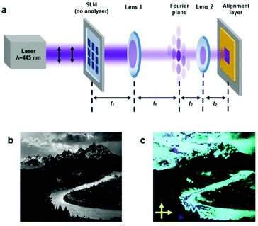
The optical design is shown in schematic form in Fig. 1(a). The 445 nm laser diode beam is s-polarized, spatially filtered, collimated, and apodized, before being transmitted through the spatial light modulator (SLM). An inexpensive, commercially available SLM is used (HoloEye LC-2002; twisted nematic (TN) mode). It consists of a display-resolution array of pixels (800 × 600), each of which is independently addressed by a grayscale signal of 8-bit depth determining the applied electric field, and thus the amount by which the incident linear polarization is rotated. Thus, the transmitted light has spatially patterned polarization angle but uniform intensity (since no analyzer is placed behind the SLM).Subsequently, a 4f lens relay images the SLM onto the target. This configuration provides easy access to the Fourier plane, where an amplitude mask is used to filter out unwanted higher diffraction orders attributed to the non-unity fill factor of the periodic array of SLM pixels.17 The 4f relay is accompanied by demagnification which can be considered advantageous in this implementation, allowing for the pixel size to be easily modified. In principle, a reduction in exposure area is exactly compensated by an increased irradiance and thus reduced exposure time, for no net penalty to the overall throughput of the patterning process.
To demonstrate arbitrary patterning of liquid crystalline materials afforded by the ability to independently address the more than 106 pixels, a grayscale image (Fig. 1b) is recorded into an alignment cell and subsequently filled with liquid crystal monomer (Fig. 1). The surface is coated with a commercial photoalignment material (PAAD-22, BEAM Co) following procedures reported in ref. 13. The SLM plane is imaged onto a target surface, with 2![[thin space (1/6-em)]](https://www.rsc.org/images/entities/char_2009.gif) :
:![[thin space (1/6-em)]](https://www.rsc.org/images/entities/char_2009.gif) 1 demagnification so that the pixel spacing in the target plane is nominally 16 μm. The approximately 1 cm2 area was patterned by exposure with ∼100 mW cm−2 of 445 nm irradiation for 10 seconds. For comparison, preparing this pattern at this size scale using the raster method reported in ref. 13 would typically take more than 30 min. The method of ref. 18, using successive exposures modulated by a DMD, would also take approximately 30 min, based on reported parameters.
1 demagnification so that the pixel spacing in the target plane is nominally 16 μm. The approximately 1 cm2 area was patterned by exposure with ∼100 mW cm−2 of 445 nm irradiation for 10 seconds. For comparison, preparing this pattern at this size scale using the raster method reported in ref. 13 would typically take more than 30 min. The method of ref. 18, using successive exposures modulated by a DMD, would also take approximately 30 min, based on reported parameters.
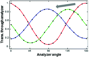
The effectiveness of polarization modulation of the SLM was characterized. With the SLM placed between a polarizer and analyzer, a grayscale signal is applied uniformly to all pixels and the transmitted intensity is measured as a function of analyzer angle. The result, shown in Fig. 2, confirms that the incident s-polarization can be rotated through more than 90° while still maintaining a low ellipticity (<10%). Thus, not all linear polarization angles are accessible, although we will show below that the available range is still sufficient to implement many director profiles of interest including topological defects. Complete access to all possible polarization angles could be implemented via a more complicated double-pass layout, following ref. 19 or 20.
The size of the resolvable local volume elements (voxels) within a “programmed” LCN or LCE defines the lower bound for the scale of miniaturized mechanical elements prepared with these methods. To provide insight into the resolution limits, we make a number of best-case simplifying assumptions, following the analysis in ref. 21, and then compute the effect of Frank elastic energy minimization on voxel resolution. First, the Frank free elastic energy density of a director profile ![[n with combining right harpoon above (vector)]](https://www.rsc.org/images/entities/i_char_006e_20d1.gif) is given by the familiar expression:
is given by the familiar expression:
 | (1) |
![[n with combining right harpoon above (vector)]](https://www.rsc.org/images/entities/i_char_006e_20d1.gif) has a purely azimuthal orientation φ(x,y,z), where the z-direction is normal to the alignment surfaces:
has a purely azimuthal orientation φ(x,y,z), where the z-direction is normal to the alignment surfaces: | (2) |
 | (3) |
 will be minimized when the 3D director profile satisfies dF/dφ = 0.
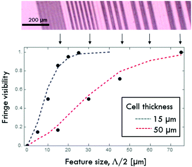
This condition is solved numerically for the first case of interest: the region near a border between two arbitrarily sharp alignment pixels of incompatible orientation (e.g. voxels in which the director is 90° offset from one another). As seen in Fig. 3(a), near the alignment surfaces the director reproduces this sharp transition, but farther from the surfaces, the director exhibits more gradual variation. Generalizing to three dimensions, consider a single alignment pixel surrounded on all sides by pixels of incompatible orientation. In this case, the director profile will maintain this pixel's templated alignment only within an hourglass-shaped volume, as shown in Fig. 3(b), rather than within a perfectly cuboidal voxel. This effectively limits the lateral feature resolution to the order of the cell thickness.
The projection system described in Fig. 1 can experimentally validate this resolution limit. To this end, we record binary gratings at various spatial frequencies and measure the fringe visibility through crossed polarizers, taking the standard definition
 | (4) |
A direct visualization of this blurring effect is provided by imaging an ISO-standard resolution test pattern (Fig. 5a) onto an alignment surface. First, the alignment surface itself is visualized by examining a sub-micron spin-coated mesogen layer, following procedures described in ref. 13. This shows distinct, crisp patterning of the pixels at the surface (Fig. 5b). Next, identical photopatterning is performed on a 15 μm thick liquid crystal cell. Here the effect of orientational relaxation through the cell volume is clearly visible (Fig. 5c) as a smoothing of feature lines (e.g. the pixels/voxels).
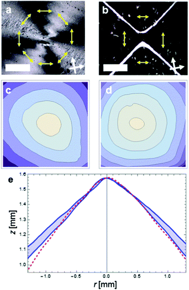
Next, we demonstrate that this system can pattern director profiles of interest to realize complex 3D shape change. A profile with a topological defect of charge +1 forms a conical actuator.22 Such +1 defects have previously been implemented with varying azimuthal director profiles,13 but theoretical predictions suggest that a similar conical actuated shape can be realized from “segmented” defect profiles with only a few uniform regions of discretized orientation.23 We pattern an LCE film with such a segmented defect profile, chosen so that all required polarization angles fall within the limited modulation range of the optical system. The resulting conical deformation forms a shape that is similar to that produced from a film with a continuously varying profile. In this way, we show here that +1 topological defects prepared from segmented or continuous director profiles exhibit nearly identical shape deformations.
Finally, we show that the voxel resolution limit inherent to these materials translates to a limit on the achievable size of actuating topological defects. Here, we reproduce the same +1 topological charge defect as before, but at a much smaller scale, so that the effective feature sizes approach the voxel resolution limit (on the order of the cell thickness). Fig. 7 shows the result of recording successively smaller isolated defect patterns into the same LCE formulation as above, with 15 μm cell thickness. For defect patterns down to 120 μm nominal diameter, the patterned director profile in the LCE is clearly visible under crossed polarizers and a well-defined cone actuates upward upon heating. Smaller defect patterns (Fig. 7c) do not retain the alignment due to the high Frank elastic energy penalties and yield a unresolvable pattern in the material that does not deform upon heating.
Materials and methods
Sample preparation
Alignment cells were self-prepared from glass slides (Colorado Concepts). Slides were spin-coated with photoalignment material, PAAD-22 (BEAM Co., 0.3 wt% in dimethylformamide). The cell gap was controlled by mixing 15 μm thick (except where otherwise specified) glass rod spacers into an optical adhesive.Photopatterning was performed using a spatially filtered 445 nm DPSS laser and a twisted-nematic SLM (HoloEye LC2002). Cells were filled within 24 hours of photopatterning.
The polymerized samples examined in Fig. 4 and 5 were prepared using RM82 ((1,4-bis-[4-(6-acryloyloxyhexyloxy)benzoyloxy]-2-methylbenzene, Synthon)) doped with 1 wt% photoinitiator (Irgacure 651, BASF). Cells were filled at 135 °C, then cooled to 90 °C, where photoinitiated polymerization was undertaken with 50–80 mW cm−2 of 365 nm light (Exfo) for 3 min.
The freestanding films examined in Fig. 6 and 7 were prepared using a previously reported LCE formulation24 consisting of a 0.5![[thin space (1/6-em)]](https://www.rsc.org/images/entities/char_2009.gif) :
:![[thin space (1/6-em)]](https://www.rsc.org/images/entities/char_2009.gif) 1
1![[thin space (1/6-em)]](https://www.rsc.org/images/entities/char_2009.gif) :
:![[thin space (1/6-em)]](https://www.rsc.org/images/entities/char_2009.gif) 1 molar ratio mixture of the following: RM82 (as above); 1,2-ethanedithiol (Sigma-Aldrich); and M05006 (2-methyl-1,4-phenylene bis(4-(3-(allyloxy)propoxy)benzoate, Synthon)). 1 wt% photoinitiator Irgacure 651 was added. Cells were filled at 100 °C, then cooled to 35 °C, whereupon photoinitiated polymerization was induced with 50–80 mW cm−2 of 365 nm light (Exfo) for 20 min.
1 molar ratio mixture of the following: RM82 (as above); 1,2-ethanedithiol (Sigma-Aldrich); and M05006 (2-methyl-1,4-phenylene bis(4-(3-(allyloxy)propoxy)benzoate, Synthon)). 1 wt% photoinitiator Irgacure 651 was added. Cells were filled at 100 °C, then cooled to 35 °C, whereupon photoinitiated polymerization was induced with 50–80 mW cm−2 of 365 nm light (Exfo) for 20 min.
 | ||
| Fig. 6 Conical deformations arising from LCE films imprinted with director profiles described by +1 topological charge. Top: Polarized optical microscopy of LCE films showing (a) continuously varying profile, via raster photopatterning as in ref. 13 and (b) segmented defect with four uniform segments, via the SLM-based photopatterning described here. Scale bars: 100 μm. (c) and (d) The corresponding deformed shapes upon heating to 175 °C, as measured by optical 3D scanner. (e) Various radial profiles of the segmented defect (blue) show comparable shape and actuation distance to the continuous defect (red). Films are 50 μm thick; formulation is as described in ref. 24. | ||
 | ||
| Fig. 7 Actuating defects realized at sub-mm scale, approaching the voxel resolution limit. Above: Polarizing optical microscope images of successively smaller patterned defects, with nominal diameters of (a) 160 μm, (b) (a) 120 μm, and (c) 80 μm (image width: 200 μm). Below: The corresponding deformations upon heating to 150 °C, as measured by 3D optical scanning. Note that for the smallest defect (c), Frank elastic energy penalties dominate, and the LCE is mostly polydomain and exhibits no deformation. LCE film is 15 μm thick; material formulation is as described in ref. 24. | ||
Characterization
Quantitative measurements of the deformed shapes were obtained using a Keyence VR-3200 optical 3D scanner. Before scanning, samples were spray-coated with an opaque antireflective coating (“3D Scan Spray”, Helling), since they would otherwise be optically transparent.Conclusions
A rapid and scalable approach to photopatterning surface alignment is reported and employed to prepare voxelated LCNs and LCEs. The optical system requires only simple projection optics and a twisted-nematic SLM, which are available off-the-shelf or can be salvaged from an LCD projector.25 In this way, this method is facile and easily accessible to non-specialists and may enable more rapid exploration of the opportunity space afforded by these materials.As we detail hereto, surface alignment methods inherently have a voxel resolution limit defined not by the optical feature sizes, but rather by director variation throughout the depth of the cell. Experimental measurements of resolution are shown to be reasonably well explained by a simple model of orientational relaxation based on Frank free elastic energy. This effect imposes a minimum achievable size on actuating topological defects and other features of interest. It also acts to smooth out director discontinuities at the interfaces between nominally incompatible domains; thus, it is relevant to efforts to optimize topology for designed curvatures or hinge angles.
Acknowledgements
The authors acknowledge funding from the Air Force Office of Scientific Research and the Materials and Manufacturing Directorate of the Air Force Research Laboratory.Notes and references
- T. H. Ware, J. S. Biggins, A. F. Shick, M. Warner and T. J. White, Localized soft elasticity in liquid crystal elastomers, Nat. Commun., 2016, 7, 10781 CrossRef PubMed.
- S. V. Serak, D. E. Roberts, J.-Y. Hwang, S. R. Nersisyan, N. V. Tabiryan, T. J. Bunning, D. M. Steeves and B. R. Kimball, Diffractive waveplate arrays [Invited], JOSA B, 2017, 34, B56 CrossRef.
- J. Küpfer and H. Finkelmann, Nematic liquid single crystal elastomers, Makromol. Chem., Rapid Commun., 1991, 12, 717 CrossRef.
- C. E. Hoyle, T. Watanabe and J. B. Whitehead, Anisotropic network formation by photopolymerization of liquid crystal monomers in a low magnetic field, Macromolecules, 1994, 27, 6581 CrossRef CAS.
- D. L. Thomsen, P. Keller, J. Naciri, R. Pink, H. Jeon, D. Shenoy and B. R. Ratna, Liquid crystal elastomers with mechanical properties of a muscle, Macromolecules, 2001, 34, 5868 CrossRef CAS.
- A. J. Pidduck, S. D. Haslam, G. P. Bryan-Brown, R. Bannister and I. D. Kitely, Control of liquid crystal alignment by polyimide surface modification using atomic force microscopy, Appl. Phys. Lett., 1997, 71, 2907 CrossRef CAS.
- T. Seki, S. Nagano and M. Hara, Versatility of photoalignment techniques: from nematics to a wide range of functional materials, Polymer, 2013, 54, 6053 CrossRef CAS.
- O. Yaroshchuk and Y. Reznikov, Photoalignment of liquid crystals: basics and current trends, J. Mater. Chem., 2012, 22, 286 RSC.
- W. M. Gibbons, P. J. Shannon, S.-T. Sun and B. J. Swetlin, Surface-mediated alignment of nematic liquid crystals with polarized laser light, Nature, 1991, 351, 49 CrossRef CAS.
- M. McConney, A. Martinez, V. Tondiglia, K. Lee, D. Langley, I. Smalyukh and T. J. White, Topography from topology: photoinduced surface features generated in liquid crystal polymer networks, Adv. Mater., 2013, 25, 5880 CrossRef CAS PubMed.
- G. P. Crawford, J. N. Eakin, M. D. Radcliffe, A. Callan-Jones and R. A. Pelcovits, Liquid-crystal diffraction gratings using polarization holography alignment techniques, J. Appl. Phys., 2005, 98, 123102 CrossRef.
- Y. Guo, M. Jiang, C. Peng, K. Sun, O. Yaroshchuk, O. Lavrentovich and Q.-H. Wei, High-Resolution and High-Throughput Plasmonic Photopatterning of Complex Molecular Orientations in Liquid Crystals, Adv. Mater., 2016, 28, 2352 CrossRef.
- T. H. Ware, M. E. McConney, J. J. Wie, V. P. Tondiglia and T. J. White, Voxelated liquid crystal elastomers, Science, 2015, 347, 982 CrossRef CAS PubMed.
- M. N. Miskiewicz and M. J. Escuti, Direct-writing of complex liquid crystal patterns, Opt. Exp., 2014, 22, 12691 CrossRef CAS PubMed.
- Y. Xia, G. Cedillo-Servin, R. D. Kamien and S. Yang, Guided Folding of Nematic Liquid Crystal Elastomer Sheers into 3D via Patterned 1D Microchannels, Adv. Mater., 2016, 28, 9637 CrossRef CAS PubMed.
- A. Ogiwara and T. Hirokari, Formation of anisotropic diffraction gratings in a polymer-dispersed liquid crystal by polarization modulation using a spatial light modulator, Appl. Opt., 2008, 47, 3015 CrossRef CAS PubMed.
- M. Agour, E. Kolenovic, C. Falldorf and C. von Kopylow, Suppression of higher diffraction orders and intensity improvement of optically reconstructed holograms from a spatial light modulator, J. Opt. A: Pure Appl. Opt., 2009, 11, 105405 CrossRef.
- C. Culbreath, N. Glazar and H. Yokoyama, Note: Automated maskless micro-multidomain photoalignment, Rev. Sci. Instrum., 2011, 82, 126107 CrossRef PubMed.
- T. K. Ewing, S. V. King, H. M. Masterson, N. Gonzales and D. Elshof, Development of a polarization hyperspectral image projector, in SPIE Defense, Security, and Sensing, 2012.
- I. Moreno, J. A. Davis, T. M. Hernandez, D. M. Cottrell and D. Sand, Complete polarization control of light from a liquid crystal spatial light modulator, Opt. Exp., 2012, 20, 364 CrossRef CAS PubMed.
- K. Kawai, T. Sasaki, K. Noda, N. Kawatsuki and H. Ono, Simple fabrication of liquid crystalline grating cells with homogeneous and twisted nematic structures and effects of orientational relaxation on diffraction properties, Appl. Opt., 2014, 53, 3679 CrossRef PubMed.
- C. Mostajeran, M. Warner, T. H. Ware and T. J. White, Encoding Gaussian curvature in glassy and elastomeric liquid crystal solids, Proc. R. Soc. A, 2016, 472, 20160112 CrossRef PubMed.
- C. D. Modes and M. Warner, Blueprinting nematic glass: Systematically constructing and combining active points of curvature for emergent morphology, Phys. Rev. E: Stat., Nonlinear, Soft Matter Phys., 2011, 84, 021711 CrossRef CAS PubMed.
- T. H. Ware, Z. P. Perry, C. M. Middleton, S. T. Iacono and T. J. White, Programmable liquid crystal elastomers prepared by thiol-ene photopolymerization, ACS Macro Lett., 2015, 4, 942 CrossRef CAS.
- D. Huang, H. Timmers, A. Roberts, N. Shivaram and A. S. Sandhu, A low-cost spatial light modulator for use in undergraduate and graduate optics labs, Am. J. Phys., 2012, 80, 211 CrossRef.
Footnote |
| † Also with Azimuth Corporation, 4027 Colonel Glenn Hwy, Beavercreek, Ohio 45431, USA. |
| This journal is © The Royal Society of Chemistry 2017 |


