 Open Access Article
Creative Commons Attribution 3.0 Unported Licence
A simple, low-cost CVD route to thin films of BiFeO3 for efficient water photo-oxidation†
Savio J. A.
Moniz
ab,
Raul
Quesada-Cabrera
a,
Christopher S.
Blackman
*a,
Junwang
Tang
b,
Paul
Southern
c,
Paul M.
Weaver
d and
Claire J.
Carmalt
a
aMaterials Chemistry Centre, Department of Chemistry, University College London, 20 Gordon Street, London, WC1H 0AJ, UK. E-mail: c.blackman@ucl.ac.uk
bDepartment of Chemical Engineering, University College London, Torrington Place, London, WC1E 7JE, UK
cUCL Healthcare Biomagnetics Laboratories, 21 Albemarle Street, London, W1S 4BS, UK
dNational Physical Laboratory, Hampton Road, Teddington, Middlesex, TW11 0LW, UK
First published on 20th December 2013
Abstract
A novel method for preparation of BiFeO3 films via a simple solution-based CVD method is reported using for the first time a single-source heterobimetallic precursor [CpFe(CO)2BiCl2]. BiFeO3 films display ferroelectric and ferromagnetic ordering at room temperature and possess direct band-gaps between 2.0 and 2.2 eV. Photocatalytic testing for water oxidation revealed high activities under UVA (365 nm) and simulated solar irradiation, superior to that exhibited by a commercial standard (Pilkington Activ® TiO2 film) resulting in an apparent quantum yield of ∼24%.
Introduction
Water photolysis for H2 fuel generation has the potential to meet increasing energy demands whilst reducing the emission of harmful greenhouse gases into the atmosphere. Water photolysis can be considered to be composed of two half reactions, water oxidation (to O2) and water reduction (to H2). However, water oxidation is widely considered to be more challenging given the fact that generation of one molecule of O2 requires four holes, generated on a timescale five orders of magnitude slower than the two electron proton reduction to H2.1,2 Therefore the search for a stable, efficient water oxidation photocatalyst is widely regarded to be significant for large-scale water photolysis. The most commonly used materials for photocatalytic water splitting are binary transition metal oxides but the band-gaps of these materials (over 3.0 eV) are too high to serve as efficient photocatalysts under visible light irradiation.3,4 Perovskite bismuth ferrite (BiFeO3, “BFO”) exhibits a direct band-gap of approximately 2.2 eV and is an active photocatalyst;5–7 BiFeO3 nanowires have been demonstrated to be promising oxygen evolution catalysts exhibiting high efficiencies under UV-light irradiation, and very recently Au–BiFeO3 nanowires have been reported to be highly active for oxygen evolution under visible light (λ > 380 nm) irradiation.8,9Chemical Vapour Deposition (CVD) has many potential advantages for deposition of BiFeO3 thin films including excellent substrate coverage, low-cost, ease of scale-up, control over thickness and morphology and high throughput capabilities, however the growth of phase-pure BiFeO3 films using chemical deposition techniques is challenging.10–12 It has been suggested that single-source heterometallic precursors could be exploited in order to improve stoichiometry control in multicomponent materials.12,13 However no examples for BiFeO3 thin films appear in the literature despite the availability of a number of bimetallic bismuth-iron containing complexes, i.e. [Bi2(Hsal)6·M(acac)3] (M = Al, V, Cr, Fe, Co)14 and [Bi2M(hfac)8] (M = Mn, Fe, Co, Ni, Cu, Zn)15 which could serve as potential precursors. Here, we describe the growth of BiFeO3 films onto a variety of substrates via a simple, low-cost solution based aerosol assisted (AA)CVD process utilizing the single-source precursor [CpFe(CO)2BiCl2] (Cp = cyclopendienyl, C5H5). AACVD is advantageous as it does not rely upon the use of highly volatile precursors, essential for typically high molecular weight heterometallic cluster compounds.16 Post-deposition heat treatment of as-deposited films resulted in pure BiFeO3 at 700 °C, confirmed via XRD, low temperature Raman and XPS spectroscopy. BiFeO3 films displayed the expected ferroelectric and ferromagnetic behavior and possessed direct band-gaps of ∼2.1 eV and we have demonstrated the films to be highly active photocatalysts for water oxidation under simulated solar irradiation. This new synthetic methodology enables large area thin film deposition, and hence is relevant for high volume applications such as solar driven water oxidation or organic pollutant degradation for water treatment.
Experimental
Detailed experimental information on film analysis and photochemical measurements are provided in ESI.†Precursor synthesis
The bimetallic molecular precursor [{Cp(CO)2Fe}BiCl2] was synthesised according to the literature from a simple equimolar reaction of [CpFe(CO)2]2 and BiCl3 in dichloromethane, and possessed identical NMR and IR spectra to those previously reported.17CVD
AACVD reactions were carried out using an in-house built cold-wall CVD described elsewhere.18,19 Nitrogen (99.96%) was obtained from BOC and used as supplied. AACVD experiments were initially conducted on SiCO cated float glass substrates (150 mm × 45 mm × 3 mm) supplied by Pilkington Glass Ltd (NSG group). The glass substrates were cleaned thoroughly in commercial washing up detergent, dried, and then cleaned with isopropanol then dried using a heat gun. In order to anneal films to temperatures greater than 600 °C, depositions were carried out on 20 mm × 20 mm × 2 mm Corning 1737 AMLCD alkaline-earth boro-aluminosilicate transparent glass substrates. For ferroelectric measurements, films were deposited onto silicon wafers which were sputtered for 180 seconds with a thin layer of platinum (argon pressure 0.1 torr, current 25 mA) prior to use, with film deposition onto the platinum. 150 mg (0.33 mmol) of [CpFe(CO)2BiCl2] precursor dissolved in ca. 40 cm3 dry THF was used for each deposition. The nitrogen gas flow through the precursor was maintained at 0.8 l min−1 and regulated using a calibrated flow meter. Annealing was carried out in air for two hours at a heating ramp rate of 10 °C min−1. For each annealing experiment a fresh sample deposited via AACVD at a substrate temperature of 300 °C was used.Photoelectrochemical measurements
Chronoamperometry measurements were conducted using a potentiostat, a Pyrex cell with a glass window and a mechanical light chopper. A Pt wire was used as the counter electrode and an Ag/AgCl electrode was used as the reference electrode. An aqueous 0.2 M sodium sulphate (Na2SO4) solution was purged for 15 minutes with argon and was used as the electrolyte (pH 6.5). The light source was a 150 W Xe lamp equipped with an AM 1.5G filter (100 mW cm−2, 1 Sun, Newport, USA). The cell was sealed with a rubber septum. The scan rate was 10 mV s−1. Mott–Schottky (impedance) measurements were measured in 0.2 M Na2SO4 in the dark at a frequency of 1 kHz and scan rate of 10 mV s−1. The potential was measured against an Ag/AgCl reference electrode and converted to RHE potentials using E(RHE) = E(Ag/AgCl) + (0.059 × pH) + 0.197 V.Photocatalytic oxygen evolution
Selected films were used to photo-oxidise water using sacrificial reagents (alkaline sodium persulphate) under UVA (365 nm) and simulated solar irradiation (150 W Xe lamp).20 In a typical experiment, the film was immersed in 30 cm3 aqueous solution under strong stirring conditions (55 rpm) in a quartz vessel with water-cooled walls (T = 298 K). The photo-oxidation of water is biased through immersion in a solution containing a sacrificial electron–acceptor (scavenger) composed of 0.01 M Na2S2O8 in 0.1 M NaOH.21 The MPD is comprised of a circular shaped silver electrode (counter and reference) and a platinum electrode disc (cathode) connected via a salt bridge (3 M KCl).21 The Pt electrode is protected from the test solution by a gas-permeable PTFE membrane.Results and discussion
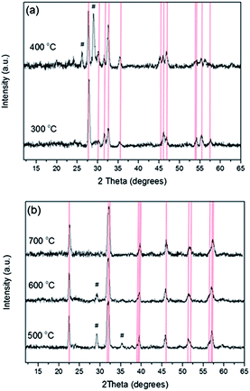
AACVD of [CpFe(CO)2BiCl2] (the TGA trace of this compound is shown in the ESI, Fig. S1†) in THF solvent at a substrate temperature of 300 °C resulted in the formation of adherent dark orange films, passing the Scotch tape test, with complete substrate coverage. Compositional analysis via WDX revealed these films contained 74 at% bismuth, 23 at% iron and 3 at% chlorine. X-ray diffraction showed only the presence of Bi24Fe2O39 (Fig. 1(a), a = b = 7.28 (4) Å, c = 5.67(2) Å, α = β = γ = 90°, space group P![[4 with combining macron]](https://www.rsc.org/images/entities/char_0034_0304.gif) 21c, PDF no. 042-0201), indicating other non-crystalline iron or bismuth rich species must also be present. No evidence of BiFeO3 formation was observed at this temperature (300 °C) via X-ray diffraction. XPS analysis revealed the presence of Fe 2p3/2 at 710.9 eV and Bi 4f7/2 at 158.7 eV, characteristic of the presence of Fe3+ and Bi3+.22,23 In order to obtain BiFeO3 the as-deposited films were annealed at a variety of temperatures up to 700 °C (between 450 and 550 °C Pilkington SiCO float glass was used and for 700 °C Corning glass was used) with the average results, after repeating the process several times to ensure reproducibility, summarised in Table 1.
21c, PDF no. 042-0201), indicating other non-crystalline iron or bismuth rich species must also be present. No evidence of BiFeO3 formation was observed at this temperature (300 °C) via X-ray diffraction. XPS analysis revealed the presence of Fe 2p3/2 at 710.9 eV and Bi 4f7/2 at 158.7 eV, characteristic of the presence of Fe3+ and Bi3+.22,23 In order to obtain BiFeO3 the as-deposited films were annealed at a variety of temperatures up to 700 °C (between 450 and 550 °C Pilkington SiCO float glass was used and for 700 °C Corning glass was used) with the average results, after repeating the process several times to ensure reproducibility, summarised in Table 1.
| Annealing temp. °C | Phase(s) obtained via XRD | At% Bi![[thin space (1/6-em)]](https://www.rsc.org/images/entities/char_2009.gif) : :![[thin space (1/6-em)]](https://www.rsc.org/images/entities/char_2009.gif) Fe (from WDX) Fe (from WDX) |
Av. film thickness/nm | Band-gap/eV | At% Cl contamination (from WDX) |
|---|---|---|---|---|---|
| 300 (as deposited) | Bi24Fe2O39 | 74![[thin space (1/6-em)]](https://www.rsc.org/images/entities/char_2009.gif) : :![[thin space (1/6-em)]](https://www.rsc.org/images/entities/char_2009.gif) 23 23 |
1700 | n/a | 3 |
| 400 | Bi24Fe2O39 + Bi2Fe4O9 | 60![[thin space (1/6-em)]](https://www.rsc.org/images/entities/char_2009.gif) : :![[thin space (1/6-em)]](https://www.rsc.org/images/entities/char_2009.gif) 38 38 |
1580 | n/a | 2 |
| 500 | BiFeO3 + Bi2Fe4O9 | 58![[thin space (1/6-em)]](https://www.rsc.org/images/entities/char_2009.gif) : :![[thin space (1/6-em)]](https://www.rsc.org/images/entities/char_2009.gif) 41 41 |
1110 | 2.0 | <1 |
| 600 | BiFeO3 + Bi2Fe4O9 | 53![[thin space (1/6-em)]](https://www.rsc.org/images/entities/char_2009.gif) : :![[thin space (1/6-em)]](https://www.rsc.org/images/entities/char_2009.gif) 47 47 |
680 | 2.2 | 0 |
| 700 | BiFeO3 | 51![[thin space (1/6-em)]](https://www.rsc.org/images/entities/char_2009.gif) : :![[thin space (1/6-em)]](https://www.rsc.org/images/entities/char_2009.gif) 49 49 |
320 | 2.1 | 0 |
Post-deposition annealing at increasing temperature led to a decrease in film thickness and relative loss of bismuth (to iron), most likely as bismuth or bismuth oxide,24 and progressive conversion of Bi24Fe2O39 to Bi2Fe4O9 and subsequently to BiFeO3 in agreement with the phase diagram constructed by Scott25 and Lu.26 Raising the annealing temperature to 700 °C caused the Bi![[thin space (1/6-em)]](https://www.rsc.org/images/entities/char_2009.gif) :
:![[thin space (1/6-em)]](https://www.rsc.org/images/entities/char_2009.gif) Fe ratio to become near unity (Bi 51 at%, Fe 49 at%) and the appearance of the films changed from dark orange (as-deposited) to bright orange. At 700 °C BiFeO3 was the only phase present via XRD [Fig. 1(b), a = b = 5.588(4) Å, c = 13.913 (6) Å, space group R3c, bulk BiFeO3a = b = 5.57414 (4) Å, c = 13.85882 (12) Å, PDF = 014-0181].27 Raman analysis further confirmed the assignment of phase pure BiFeO3 (ESI, Fig. S2†). Chlorine contamination from the precursor was initially high for the as-deposited film and for those annealed at 400 °C (2.5 and 1.6 at% respectively), however this contamination decreased dramatically as a function of annealing temperature and by 600 °C was below the detection limit of WDX.
Fe ratio to become near unity (Bi 51 at%, Fe 49 at%) and the appearance of the films changed from dark orange (as-deposited) to bright orange. At 700 °C BiFeO3 was the only phase present via XRD [Fig. 1(b), a = b = 5.588(4) Å, c = 13.913 (6) Å, space group R3c, bulk BiFeO3a = b = 5.57414 (4) Å, c = 13.85882 (12) Å, PDF = 014-0181].27 Raman analysis further confirmed the assignment of phase pure BiFeO3 (ESI, Fig. S2†). Chlorine contamination from the precursor was initially high for the as-deposited film and for those annealed at 400 °C (2.5 and 1.6 at% respectively), however this contamination decreased dramatically as a function of annealing temperature and by 600 °C was below the detection limit of WDX.
XPS of a film annealed at 700 °C showed the presence of iron in the +3 oxidation state [Fe 2p3/2, 711.3 eV (Fig. S3, ESI†)] with the expected Fe3+ satellite peak observed at 718.9 eV.12 Oxygen under stoichiometry, leading to a co-existence of Fe2+ and Fe3+ species, leads to broadening of the Fe 2p3/2 peak to lower energies but this was not observed in our samples. A single Bi 4f7/2 ionisation at 159.4 eV was observed, characteristic of bismuth in the +3 oxidation state, as expected for BiFeO3.23 No chlorine contamination was detected via XPS; carbon was observed on the surface but decreased upon etching indicating it to be surface contamination. Analysis of the Bi 4f, Fe 2p and O 1s (B.E. of O 1s = 530.2 eV) peak areas after etching indicated the presence of the three components in an approximate 1![[thin space (1/6-em)]](https://www.rsc.org/images/entities/char_2009.gif) :
:![[thin space (1/6-em)]](https://www.rsc.org/images/entities/char_2009.gif) 1
1![[thin space (1/6-em)]](https://www.rsc.org/images/entities/char_2009.gif) :
:![[thin space (1/6-em)]](https://www.rsc.org/images/entities/char_2009.gif) 3 ratio, commensurate with BiFeO3.
3 ratio, commensurate with BiFeO3.
As-deposited films (300 °C) possessed a globular morphology, with average particle diameters of 100 nm (ESI, Fig. S4†). Heat treatment at higher temperatures led to coalescence of particles (ESI, Fig. S5†), whilst at 700 °C (Fig. 2(a)) the sintering of the particles led to films becoming rougher and less uniform; AFM (Fig. 2(c and d)) showed the films to be comprised of larger aggregates with a rough texture (root mean squared roughness (rms) = 62 nm) in agreement with SEM. Hence films synthesised by this route are likely to possess high surface areas for enhanced catalytic activity.
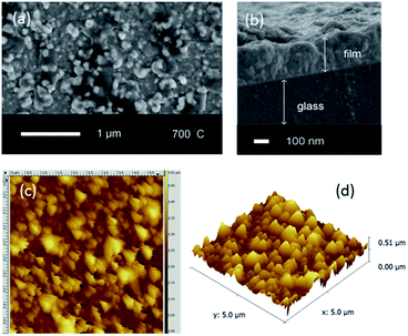 | ||
| Fig. 2 (a) A typical top-down SEM image (b) side-on SEM image, (c) a 5 μm field size AFM image and (d) the corresponding 3D AFM image of the BiFeO3 film formed after annealing at 700 °C. | ||
Films of BiFeO3, grown by deposition directly onto 1 cm2 Pt/SiO2/Si wafers via AACVD followed by annealing at 700 °C, displayed a maximum polarisation of 8.7 μC cm−2, providing an effective relative permittivity of almost 800 (ESI, Fig. S6†). The maximum polarisation is smaller than that for single crystal or epitaxial film bismuth ferrite (around 50 μC cm−2),28 but higher than those obtained for BiFeO3 films grown via sol–gel processing (Pr = 1.8 μC cm−2)29 or PLD (Pr = 0.83 μC cm−2).30 Measurement of the magnetic properties of a 320 nm thick film (ESI, Fig. S7†) revealed that the M–H hysteresis loops recorded at 5 K and 300 K were similar to those reported previously28 (after subtracting the diamagnetic contribution from the substrate), i.e. these BiFeO3 films show weak ferromagnetic behaviour with well-saturated hysteresis loops at both temperatures. Upon raising the temperature to 300 K the coercivity was measured as 135 Oe and −115 Oe with an expected decrease in saturation magnetisation to 8.9 emu cm−3. The coercivity is lower than that observed for a 70 nm thick BiFeO3 film grown via PLD (200 Oe)31 although a decrease in magnetisation as a function of increasing film thickness was observed, from 150 emu cm−3 for a 70 nm thick film to 5 emu cm−3 for a 400 nm thick film, consistent with our measurement of film thickness (∼320 nm). Spin-glass behaviour was also observed from M–T measurements (ESI†).
A typical transmission spectrum of a film containing BiFeO3 as the only crystalline phase (ESI, Fig. S8†) shows over 70% transmittance in the 800–2500 nm range with the cut-off from the glass substrate coming into effect below 380 nm. The band-gaps of the films were calculated using Tauc plots (see Fig. S9, ESI†).32 Extrapolating the linear part of the plot to the x-axis for a phase-pure sample resulted in an intercept of approximately 2.1 eV, in good agreement with experimentally derived band-gap values for BiFeO3; films with smaller band-gaps (2.0 eV) contained impurity Bi2Fe4O9 and are in line with the expected decrease in band-gap of Bi2Fe4O9 compared to BiFeO3.33,34
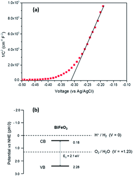
For photoelectrochemical (PEC) measurements BiFeO3 was grown on FTO coated glass substrates. In order to estimate the relative levels of the conduction and valence bands of BiFeO3 electrical impedance measurements were carried out from which the flat-band potential (Efb) was measured. Fig. 3(a) displays the Mott–Schottky plot for a BiFeO3 film deposited onto FTO coated glass. For n-type semiconductors the flat-band potential (Efb) is considered to be located just under the conduction band, hence Efb of BiFeO3 was estimated to be −0.31 V (vs. Ag/AgCl) or + 0.18 V (vs. RHE),35,36 which is similar to values previously estimated from atomic electronegativities.37 Based upon this value and that determined for the band-gap of BiFeO3 (2.1 eV), a band diagram (Fig. 3(b)) was constructed, indicating BiFeO3 has significant overpotential for photocatalytic water oxidation.
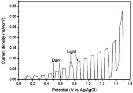
The photoanodic activity of BiFeO3 was investigated using PEC measurements and also via oxygen evolution using a sacrificial electron acceptor solution. Fig. 4 shows the chronoamperometry measurement obtained from a BiFeO3 photoelectrode under 1 Sun (100 mW cm−2) AM 1.5G illumination. There is a steady increase in photocurrent with increasing potential and the photocurrent at 1.0 V vs. Ag/AgCl was appreciable (ca. 0.1 mA cm−2 (103 μA cm−2)). This value is similar to that obtained by Yu et al.38 for BiFeO3 films deposited via PLD onto platinised silicon substrates (∼90 μA cm−2 at 1.0 V vs. Ag/AgCl, 400 W Xe lamp) but substantially higher than the current density reported for hydrothermally synthesised BiFeO3 nanocube electrodes in pure water (5.2 μA cm−2 at 1.0 V vs. SCE, 500 W Hg lamp)39 and higher than BFO/SRO/STO films grown via sputtering (10 μA at 0.64 V vs. Ag/AgCl).40
In order to verify the water oxidation activity, tests for oxygen evolution from a Na2S2O8/NaOH sacrificial solution were carried out using an MPD cell (see ESI† for more details) and compared to a commercial standard photocatalyst (Pilkington Activ® glass).41 The overall photocatalytic reaction is given by eqn (1).
| 2S2O82− + 2H2O → 4SO42− + 4H+ + O2 | (1) |
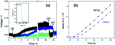
Fig. 5 shows the typical output of the MPD cell during photo-generation of oxygen on BiFeO3 films under full-arc Xe-lamp irradiation (150 W) with the corresponding amounts of oxygen produced during the first 10 h irradiation shown in Fig. 5(b). The output reading shows an increase in voltage during an initial illumination period followed by a plateau around 0.05 V, indicating steady oxygen production during prolonged irradiation (above 20 h). A small drop in the signal when turning on the Xe lamp, attributed to an interruption of the electrical supply, was observed however this did not affect the observed rate. Signal drift was also observed after prolonged use of the MPD cell, as illustrated by the blank test carried out on uncoated glass, however signal drop was noted after switching off the light source demonstrating the oxygen evolution was a photocatalytic effect. In addition no change in voltage, i.e. no oxygen evolution, was observed in the absence of illumination. The oxygen rates and % O2 yields obtained during UVA irradiation of BiFeO3 and Activ® glass films are given in Table 2.
| Rate of O2 evolution (μmol h−1) | O2 yield (%, 365 nm) | ||
|---|---|---|---|
| Solar lamp | UVA | ||
| BiFeO3 | 0.33 | 0.023 | 24.4 |
| TiO2 (Activ) | 0.26 | 0.012 | 4.8 |
The % O2 yield of the process has been determined according to eqn (2).
| % O2 yield = (molecules formed/incident photons) × 4 (electrons) × 100% | (2) |
An average O2 yield of 24.4% (365 nm) was obtained for BiFeO3 (in the absence of co-catalyst) which represents a near 10-fold increase over optimised B-doped TiO2 films investigated under identical conditions.42 The O2 yield of the Activ® reference was ∼5% at 365 nm. It should be noted that the BiFeO3 films tested were significantly thicker (∼300 nm) than that reported for the TiO2 layer in Activ® glass (∼15 nm). XPS and X-ray diffraction patterns of the films conducted after photocatalytic testing revealed no change in composition or phase indicating that these BiFeO3 films are robust under the basic conditions of the test and do not undergo photocorrosion, which was supported by the continued measurement of oxygen evolution on prolonged irradiation and subsequent tests which proved the effect was reproducible. Visible-light tests were also carried out using UV cut-off filters under similar experimental conditions however no increase in voltage could be distinguished above the signal drift of the MPD cell. This is perhaps not surprising given the photocatalytic activity of BiFeO3 powders for oxygen evolution (from a FeCl3 solution) using visible light irradiation (500 W Hg lamp, λ > 420 nm) is less than 0.2 μmol h−1,39 and hence we are currently investigating more suitable methods for evaluating the visible light activity of BiFeO3 thin films. The high photocatalytic activity for water oxidation displayed by our BiFeO3 films may not be solely due to the high surface area of thin films; it has recently been reported that ferroelectric domains in BiFeO3 enhance charge-carrier separation through photocatalytic decomposition of AgNO3, resulting in selective Ag reduction on the surface and simultaneous oxygen evolution under visible light irradiation.43,44
Conclusions
For the first time, BiFeO3 films were grown via a simple solution-based AACVD procedure at an unprecedented low temperature using the single-source precursor [{Cp(CO)2Fe}BiCl2], followed by post-deposition annealing at elevated temperature in air. As-deposited films were characterised as containing Bi24Fe2O39via XRD; annealed films were identified as BiFeO3 by XRD and Raman spectroscopy with compositional analysis revealing bismuth to iron ratios of 1![[thin space (1/6-em)]](https://www.rsc.org/images/entities/char_2009.gif) :
:![[thin space (1/6-em)]](https://www.rsc.org/images/entities/char_2009.gif) 1. Magnetic hysteresis and ferroelectric polarisation measurements confirmed ferromagnetic and ferroelectric ordering at room temperature. Direct band-gaps between 2.0 and 2.2 eV were measured for all films. Photocatalytic testing under both UV and solar irradiation confirmed appreciable activity of BiFeO3 for the kinetically slow four hole process of water oxidation.1 Despite having a less deep valence band potential than TiO2, facile water oxidation is found, with the resultant apparent quantum yield of our samples exhibiting a near six-fold increase over a commercial standard photocatalyst (TiO2 Activ® glass) and a ten-fold increase over B-doped TiO2 films recently reported.42 Furthermore, we have demonstrated the possibility of using relatively non-volatile molecular compounds for the growth of complex heterometallic oxides via AACVD. To the best of our knowledge, no precursors of this class have previously been utilised in CVD processes.
1. Magnetic hysteresis and ferroelectric polarisation measurements confirmed ferromagnetic and ferroelectric ordering at room temperature. Direct band-gaps between 2.0 and 2.2 eV were measured for all films. Photocatalytic testing under both UV and solar irradiation confirmed appreciable activity of BiFeO3 for the kinetically slow four hole process of water oxidation.1 Despite having a less deep valence band potential than TiO2, facile water oxidation is found, with the resultant apparent quantum yield of our samples exhibiting a near six-fold increase over a commercial standard photocatalyst (TiO2 Activ® glass) and a ten-fold increase over B-doped TiO2 films recently reported.42 Furthermore, we have demonstrated the possibility of using relatively non-volatile molecular compounds for the growth of complex heterometallic oxides via AACVD. To the best of our knowledge, no precursors of this class have previously been utilised in CVD processes.
Acknowledgements
UCL/EPSRC are acknowledged for financial support. Dr Steve Firth is thanked for assistance with low temperature Raman spectroscopy. The NPL would like to acknowledge financial support from the UK's National Measurement system. Dr Emily Smith is thanked for XPS analysis under EPSRC grant EP/F019750/1: “A Coordinated Open-Access Centre for Comprehensive Materials Analysis”.Notes and references
- J. Tang, J. R. Durrant and D. R. Klug, J. Am. Chem. Soc., 2008, 130, 13885–13891 CrossRef CAS PubMed.
- D. J. Martin, N. Umezawa, X. Chen, J. Ye and J. Tang, Energy Environ. Sci., 2013, 6, 3380–3386 CAS.
- A. Bard and M. Fox, Acc. Chem. Res., 1995, 28, 141–145 CrossRef CAS.
- A. Kudo, K. Omori and H. Kato, J. Am. Chem. Soc., 1999, 121, 11459–11467 CrossRef CAS.
- F. Gao, X. Y. Chen, K. B. Yin, S. Dong, Z. F. Ren, F. Yuan, T. Yu, Z. G. Zou and J.-M. Liu, Adv. Mater., 2007, 19, 2889–2892 CrossRef CAS.
- S. Li, Y. Lin, B. Zhang and Y. Wang, J. Phys. Chem. C, 2010, 114, 2903–2908 CAS.
- X. Xu, Y.-H. Lin, P. Li, L. Shu and C.-W. Nan, J. Am. Ceram. Soc., 2011, 94, 2296–2299 CrossRef CAS.
- F. Gao, Y. Yuan, K. F. Wang, X. Y. Chen, F. Chen, J.-M. Liu and Z. F. Ren, Appl. Phys. Lett., 2006, 89, 102506 CrossRef PubMed.
- S. Li, J. Zhang, M. G. Kibria, Z. Mi, M. Chaker, D. Ma, R. Nechache and F. Rosei, Chem. Commun., 2013, 49, 5856–5858 RSC.
- S. Y. Yang, F. Zavaliche, L. Mohaddes-Ardabili, V. Vaithyanathan, D. G. Schlom, Y. J. Lee, Y. H. Chu, M. P. Cruz, Q. Zhan, T. Zhao and R. Ramesh, Appl. Phys. Lett., 2005, 87, 102903 CrossRef PubMed.
- M. Kartavtseva, O. Gorbenko and A. Kaul, Surf. Coat. Technol., 2007, 201, 9149–9153 CrossRef CAS PubMed.
- J. Thery, C. Dubourdieu, T. Baron, C. Ternon, H. Roussel and F. Pierre, Chem. Vap. Deposition, 2007, 13, 232–238 CrossRef CAS.
- A. C. Jones, J. Mater. Chem., 2002, 12, 2576–2590 RSC.
- J. H. Thurston, D. Trahan, T. Ould-Ely and K. H. Whitmire, Inorg. Chem., 2004, 43, 3299–3305 CrossRef CAS PubMed.
- E. V Dikarev, H. Zhang and B. Li, J. Am. Chem. Soc., 2005, 127, 6156–6157 CrossRef PubMed.
- P. Marchand, I. A. Hassan, I. P. Parkin and C. J. Carmalt, Dalton Trans., 2013, 42, 9406–9422 RSC.
- T. Gröer and M. Scheer, J. Chem. Soc., Dalton Trans., 2000, 647–653 RSC.
- S. Vallejos, T. Stoycheva, P. Umek, C. Navio, R. Snyders, C. Bittencourt, E. Llobet, C. Blackman, S. Moniz and X. Correig, Chem. Commun., 2011, 47, 565–567 RSC.
- S. J. A. Moniz, D. Bhachu, C. S. Blackman, A. J. Cross, S. Elouali, D. Pugh, R. Quesada Cabrera and S. Vallejos, Inorg. Chim. Acta, 2012, 380, 328–335 CrossRef CAS PubMed.
- S. J. A. Moniz, C. S. Blackman, C. J. Carmalt and G. Hyett, J. Mater. Chem., 2010, 20, 7881–7886 RSC.
- A. Mills and M. A. Valenzuela, J. Photochem. Photobiol., A, 2004, 165, 25–34 CrossRef CAS PubMed.
- T. Yamashita and P. Hayes, Appl. Surf. Sci., 2008, 254, 2441–2449 CrossRef CAS PubMed.
- V. S. Dharmadhikari, S. Sainkar, S. Badrinarayan and A. Goswami, J. Electron Spectrosc. Relat. Phenom., 1982, 25, 181–189 CrossRef CAS.
- F. Tyholdt, S. Jørgensen, H. Fjellvåg and A. E. Gunnaes, J. Mater. Res., 2005, 20, 2127–2139 CrossRef CAS.
- R. Palai, R. Katiyar, H. Schmid, P. Tissot, S. Clark, J. Robertson, S. Redfern, G. Catalan and J. Scott, Phys. Rev. B: Condens. Matter Mater. Phys., 2008, 77, 1–11 CrossRef.
- K. Feng, L.-C. Wang, J. Lu, Y. Wu and B.-G. Shen, CrystEngComm, 2013, 15, 4900 RSC.
- A. Reyes, C. Delavega, M. Fuentes and L. Fuentes, J. Eur. Ceram. Soc., 2007, 27, 3709–3711 CrossRef CAS PubMed.
- G. Catalan and J. F. Scott, Adv. Mater., 2009, 21, 2463–2485 CrossRef CAS.
- Y. Wang, Q. Jiang, H. He and C.-W. Nan, Appl. Phys. Lett., 2006, 88, 142503 CrossRef PubMed.
- V. R. Palkar, J. John and R. Pinto, Appl. Phys. Lett., 2002, 80, 1628 CrossRef CAS PubMed.
- J. Wang, J. B. Neaton, H. Zheng, V. Nagarajan, S. B. Ogale, B. Liu, D. Viehland, V. Vaithyanathan, D. G. Schlom, U. V Waghmare, N. A. Spaldin, K. M. Rabe, M. Wuttig and R. Ramesh, Science, 2003, 299, 1719–1722 CrossRef CAS PubMed.
- J. Tauc, R. Grigorovici and A. Vancu, Phys. Status Solidi B, 1966, 15, 627–637 CrossRef CAS.
- D. Cai, D. Du, S. Yu and J. Cheng, Procedia Eng., 2012, 27, 577–582 CrossRef CAS PubMed.
- Q.-J. Ruan and W.-D. Zhang, J. Phys. Chem. C, 2009, 113, 4168–4173 CAS.
- K. Sayama, A. Nomura, T. Arai, T. Sugita, R. Abe, M. Yanagida, T. Oi, Y. Iwasaki, Y. Abe and H. Sugihara, J. Phys. Chem. B, 2006, 110, 11352–11360 CrossRef CAS PubMed.
- S. J. Hong, S. Lee, J. S. Jang and J. S. Lee, Energy Environ. Sci., 2011, 4, 1781 CAS.
- S. Li, Y.-H. Lin, B.-P. Zhang, J.-F. Li and C.-W. Nan, J. Appl. Phys., 2009, 105, 054310 CrossRef PubMed.
- X. Y. Chen, T. Yu, F. Gao, H. T. Zhang, L. F. Liu, Y. M. Wang, Z. S. Li, Z. G. Zou and J.-M. Liu, Appl. Phys. Lett., 2007, 91, 022114 CrossRef PubMed.
- U. A. Joshi, J. S. Jang, P. H. Borse and J. S. Lee, Appl. Phys. Lett., 2008, 92, 242106 CrossRef PubMed.
- W. Ji, K. Yao, Y.-F. Lim, Y. C. Liang and A. Suwardi, Appl. Phys. Lett., 2013, 103, 062901 CrossRef PubMed.
- A. Mills, A. Lepre, N. Elliott, S. Bhopal, I. P. Parkin and S. A. O'Neill, J. Photochem. Photobiol., A, 2003, 160, 213–224 CrossRef CAS.
- P. Carmichael, D. Hazafy, D. S. Bhachu, A. Mills, J. A. Darr and I. P. Parkin, Phys. Chem. Chem. Phys., 2013, 15, 16788–16794 RSC.
- Y. Zhang, A. M. Schultz, P. A. Salvador and G. S. Rohrer, J. Mater. Chem., 2011, 21, 4168–4174 RSC.
- A. M. Schultz, Y. Zhang, P. A. Salvador and G. S. Rohrer, ACS Appl. Mater. Interfaces, 2011, 3, 1562–1567 CAS.
Footnote |
| † Electronic supplementary information (ESI) available: Further experimental details, DSC–TGA pattern of [{Cp(CO)2Fe}BiCl2], Raman spectrum of a pure BiFeO3 film recorded at −195 °C, XPS spectrum of the Fe 2p region of a BiFeO3 thin film after etching, top-down SEM images of Bi24Fe2O39 film deposited on glass at 300 °C, top-down SEM images of the films annealed between 400 and 650 °C, P–E hysteresis loop for a pure BiFeO3 film on Pt/SiO2/Si substrate, M–H and ZFC–FC curves for BiFeO3 film, UV-vis spectrum of a pure BiFeO3 film, corresponding Tauc plot for a BiFeO3 film. See DOI: 10.1039/c3ta14824f |
| This journal is © The Royal Society of Chemistry 2014 |

