
Alkali element (Li, Na, K, and Rb) doping of Cu2BaGe1−xSnxSe4 films†
Yongshin
Kim
 a,
Hannes
Hempel
b,
Steven P.
Harvey
c,
Nelson A.
Rivera
Jr
d,
Thomas
Unold
b and
David B.
Mitzi
*ae
a,
Hannes
Hempel
b,
Steven P.
Harvey
c,
Nelson A.
Rivera
Jr
d,
Thomas
Unold
b and
David B.
Mitzi
*ae
aDepartment of Mechanical Engineering and Materials Science, Duke University, Durham, North Carolina 27708, USA
bDepartment Structure and Dynamics of Energy Materials, Helmholtz-Zentrum Berlin für Materialien und Energie GmbH, Hahn-Meitner-Platz 1, 14109, Berlin, Germany
cRenewable and Sustainable Energy Institute, University of Colorado Boulder, Boulder Colorado 80309, USA
dDepartment of Civil and Environmental Engineering, Duke University, Durham, North Carolina 27708, USA
eDepartment of Chemistry, Duke University, Durham, North Carolina 27708, USA. E-mail: david.mitzi@duke.edu
First published on 7th June 2023
Abstract
Cu2BaGe1−xSnxSe4 (CBGTSe) represents an exemplary system within the I2–II–IV–X4 (I = Ag, Cu; II = Sr, Ba; IV = Ge, Sn; X = S, Se) family, which has been introduced to target suppressing the formation of anti-site defects and associated defect clusters within the analogous kesterite Cu2ZnSn(S,Se)4. Previous studies on CBGTSe films showed relatively low hole carrier densities (<1013 cm−3), which may limit their corresponding application as active layers within photovoltaic, thermoelectric, and optoelectronic devices. In the current study, we explore the incorporation of alkali elements (Li, Na, K, and Rb) into CBGTSe films as prospective dopants to address the low hole carrier density and to allow for property tunability. First, incorporation of Na-, K-, and Rb-dopants noticeably increases the average grain sizes for CBGTSe films, while the Li-dopant has relatively limited impact. In addition, the alkali-dopants lead to a 1 to 3 orders of magnitude increase in hole carrier density (up to 1015 cm−3 is achieved using K doping, corresponding to the alkali element yielding the highest doping efficiency). The alkali-doped films show slightly lower minority carrier lifetimes and carrier mobility values than the non-doped samples, and these values are found to follow an approximate universal dependence with carrier density (also considering data derived from other previously explored vacuum-deposited I2–II–IV–X4 chalcogenide films). As alkali-doping can significantly increase carrier densities, alkali elements can be considered useful p-type dopants for CBGTSe, as well as prospectively for other analogous I2–II–IV–X4 systems.
1. Introduction
Recently, I2–II–IV–X4 (I = Ag, Cu; II = Sr, Ba; IV = Ge, Sn; X = S, Se) compounds have been introduced to target suppressing the formation of anti-site defects and related defect clusters,1–3 which are known to be the origin of the high VOC deficit of kesterite Cu2ZnSnS4−xSex (CZTS) based solar cells.4–10 Among these compounds, Cu2BaSnS4−xSex (CBTSSe) was the first to gain attention for solar cell application due to its similarities to CZTSSe in the following aspects: CBTSSe consists of only earth-abundant and lower toxicity metals. Also, the compound offers band gap tunability (i.e., 1.55 eV ≤ Eg ≤ 1.95 eV) via controlling the ratio of S/(S + Se),11 which allows for accessing ideal values for optoelectronic and single- and multi-junction photovoltaic (PV) applications. Various thin-film synthesis studies using both solution-12–14 and vacuum-based techniques,11,15–17 as well as their photovoltaic properties,13,15,17,18 have been reported for CBTSSe. Power conversion efficiency (PCE) values as high as 6.5% have recently been achieved for solution-processed CBTSSe PV devices.18 Furthermore, CBTSSe absorbers have shown promise for photoelectrochemical cell application.12,19,20 I2–II–IV–X4 compounds have also drawn attention due to their ultralow thermal conductivities,21–23 which may be suitable for thermoelectric device application.Cu2BaGe1−xSnxSe4 (CBGTSe; x ≤ 0.7) is another less-studied material within the I2–II–IV–X4 family with the same crystal structure as CBTSSe (P31 space group), which offers a similar bandgap range (1.57–1.91 eV), this time achieved by adjusting the metal cation ratio—i.e., Sn/(Sn + Ge) (rather than focusing on anion replacement for CBTSSe). Kim et. al.24 demonstrated the first films and PV devices based on Sn-free CBGSe and revealed two possible major bottlenecks for CBGSe-based solar cells: (1) poor bulk properties (i.e., high density of deep-level defects) and (2) relatively low electron affinity, which would lead to the formation of cliff-type conduction band offset (i.e., CBO < 0 eV) with a conventional CdS buffer material. The first limitation on bulk properties suggests that the detrimental defects in the CBGSe layer are at least partially responsible for the observed large VOC deficit (Eg/q − VOC = ∼1.3 V). The second bottleneck relates to the relatively low electron affinity, leading to the formation of cliff-type CBO between the absorber and buffer layer of the solar cell, which can significantly limit the performance of solar cells due to interface recombination.25 Kim and Mitzi have also recently reported the first (Sn-containing) CBGTSe films with a smaller band gap of 1.65 eV and solar cell devices with a maximum PCE of 3.1%.26 However, the solar cells still show a large VOC deficit (∼1.0 V) with low quantum efficiencies, especially for the long wavelength regions, both of which also indicate poor recombination properties for CBGTSe. Later, as a potential approach to adjust recombination properties as well as conduction band and valence band edges, partial substitution of Cu by Ag to form Cu2−yAgyBaGe1−xSnxSe4 (ACBGTSe) has been explored.27 Up to 20% of the Cu in CBGTSe could be substituted by Ag, while above 20%, an additional orthorhombic (I222) ACBGTSe secondary phase appears. While increasing Ag content impacts average grain size and hole carrier densities, substitution by up to 20% Ag has negligible impact on band edge positions, charge carrier recombination, and transport properties, and therefore does not improve overall PV-related properties. However, it is noteworthy that all CBGTSe and ACBGTSe films, regardless of the Ag content, showed limited hole carrier density under dark conditions (p < 1013 cm−3) compared to other PV-relevant multinary chalcogenides (p = 1015 to 1017 cm−3 for CIGS28,29 and CZTS30,31). Charge carrier density is an important parameter for solar absorbers because it, not only determines the band bending (and associated depletion width) within the heterojunction, but also affects the device series resistance and quasi-Fermi level splitting (QFLS) within the light-absorbing material, which determines the maximum achievable VOC. Furthermore, carrier density can also be important for other types of device applications—e.g., controlling conductivity is critical to maximizing figure of merit, a parameter that directly relates to TE device performance.
One possible approach to enhance the hole carrier density for CBGTSe relates to the inclusion of an extrinsic element for doping. A well-known example of such doping derives from CdTe-related materials, important due to the limited carrier density of intrinsic CdTe (p = ∼1014 cm−3),32 using possible p-type dopants such as Na/Cu (on Cd sites)33–35 and P/As/Sb (on Te sites).34–37 However, up to this point, no extrinsic element doping study has been conducted for enhancing hole carrier density for CBGTSe or CBTSSe systems. One of the well-known dopants for other chalcogenide systems (e.g., CIGS and CZTS) has been alkali metals (i.e., group-1 elements),38,39 which might be targeted as p-type dopants for CBGTSe, if the elements preferentially substitute on the Ba (group-2) or Sn/Ge (group-14) sites. Notably, the alkali element column of the periodic table offers options (Li+ through Cs+) that cover a wide range of ionic radii and electronegativities. These properties may in turn impact substitution site preference (especially for the CBTSSe and CBGTSe families, given that these systems contain sites with very different coordination and size requirements) and doping efficiencies. Three approaches have been mainly used for adding alkali elements into the general family of vacuum-deposition-based chalcogenide films: (1) pre-deposition, (2) co-evaporation, and (3) post-deposition of the alkali-containing source.38 Alkali fluorides (e.g., NaF and KF) have been the most commonly used alkali source for providing alkali elements to chalcogenide films (i.e., CIGS38 and CZTS39,40), and the amount of alkali element incorporation is controlled by the total thickness of the alkali fluoride layer deposited during the deposition process. For chalcopyrite CIGSSe, the post-deposition approach has been used to incorporate alkali elements along grain boundaries for passivation—i.e., alkali elements are incorporated into only a limited portion of the film via diffusion.41,42 However, in the case where alkali elements are targeted for use as p-type dopants to impact bulk hole carrier density, the pre-deposition approach, which implies depositing a thin layer of alkali fluoride prior to the deposition of CBGTSe to involve alkali elements within the film growth process, may offer some benefits in terms of achieving a uniform film composition.
In the current study, we investigate the impact of alkali doping within CBGTSe films, prepared using a vacuum-based deposition approach and a pre-deposition doping strategy, focusing on four different alkali elements (from Li to Rb). These elements have distinct cation sizes—e.g., Li+ (0.59 Å) is comparable in ionic radius to Cu+ (0.60 Å), while K+ (1.51 Å) is close to Ba2+ (1.42 Å).43 The biggest cation within the CBGTSe system is Ba2+ (1.42 Å), and Rb+ (1.61 Å) is significantly bigger than this ion.43 Cs (1.74 Å) goes beyond the size range that we intended to study and therefore it is not considered.43 This study specifically focuses on examining (1) phase purity, film morphology, and grain structure, (2) charge carrier density and doping efficiency, (3) prospective dopant distribution within the film, and (4) charge carrier kinetics and recombination properties, which are all critical for prospective photovoltaic, optoelectronic and thermoelectric applications. Scanning electron microscopy (SEM) and X-ray diffraction (XRD) techniques enable the examination of film morphology, crystal structure, and phase purity for the alkali-doped CBGTSe films. The concentrations of the alkali elements in the CBGTSe films are determined via inductively coupled plasma mass spectrometry (ICP-MS). The alkali element distributions within the doped CBGTSe films are examined via a time-of-flight secondary ion mass spectrometry (TOF-SIMS) technique. Hall effect measurement establishes the major charge carrier type, carrier density, and Hall mobility for the non-doped and doped samples. Optical-pump terahertz-probe spectroscopy (OPTP) analyses have also been performed for the various film types to check whether the inclusion of alkali-dopants impacts charge carrier recombination and transport properties. The results reveal the effectiveness and possible limitations of using alkali elements as p-type dopants for films based on CBGTSe, as well as for analogous compounds based on related I2–II–IV–X4 chalcogenides.
2. Experimental section/methods
2.1. Thin film fabrication
Sample preparation was conducted using the following procedures: first, alkali fluoride (i.e., LiF, NaF, KF, or RbF) layers were deposited using a thermal evaporation system (Angstrom Engineering). The fluorides were deposited at a flux of approximately 6 Å min−1 targeting 1 nm, 2 nm, or 4 nm thickness (monitored using a quartz crystal microbalance) on bare quartz glass substrates. Here, the density values for LiF, NaF, KF, and RbF were assumed to be 2.638 g cm−3, 2.558 g cm−3, 2.480 g cm−3, and 3.557 g cm−3, respectively. The Z-factors were assumed to be 0.778 for LiF, and 0.949 for NaF. Because the Z-factors for both KF and RbF are unknown, they are assumed to be 1.000. After the deposition of alkali fluoride layers, the substrates were transferred into a deposition system (AJA International) equipped with a vacuum chamber, sputter guns (for the deposition of Cu, Sn, and Ge layers) and an evaporator (for Ba layers), without exposure to the ambient air. The deposition process for the CBGTSe films consists of three steps: deposition, pre-annealing, and selenization. First, Cu–Ba–Ge–Sn precursor layers were prepared by consecutive deposition of multiple stacked layers of Cu, Ge, Sn and Ba. The base pressure of the vacuum chamber was held below 1.0 × 10⁻⁷ Torr. Cu, Ge, and Sn layers were deposited by RF sputtering of Cu (99.999%, 3 inches; Kurt J. Lesker), Ge (99.999%, 3 inches; MSE Supplies), and Sn (99.999%, 3 inches; AJA International) targets at ∼2.6 W cm−2, ∼1.8 W cm−2, and ∼1.3 W cm−2 power densities, respectively, under 3 mTorr of an Ar atmosphere. The Ba layer was deposited by thermal evaporation of Ba pieces (99.7%; Strem Chemicals) under vacuum. After completing the deposition, the metallic precursor layers were pre-annealed at 580 °C for 30 min in the same vacuum chamber.24,26,27 The detailed deposition procedure is described elsewhere.24,26,27 After cooling to room temperature, the substrates were directly transferred into a N2-filled glove box without exposure to the ambient air. Then, the substrates were placed on a hotplate at a temperature of 530 °C for 60 min with extra Se (∼0.1 g) maintained under a quartz cover for selenization of the metal precursor layers. The experimental setup for the selenization process is described in detail elsewhere.12 The elemental composition ratios for the films, determined from ICP-MS, ranged between Cu/(Ba + Sn + Ge) = 1.00–1.08, Sn/(Sn + Ge) = 0.64–0.68, Ba/(Sn + Ge) = 1.01–1.06, and Se/(Cu + Ba + Sn + Ge) = 0.97–1.00.2.2. Characterizations of films
XRD patterns of the non-doped and alkali-doped CBGTSe films were acquired at room temperature using a Malvern Panalytical Empyrean diffractometer with Cu Kα radiation. SEM images were acquired using an FEI Apreo S system. Hall effect measurement was conducted using an AC Field Parallel Dipole Line Hall Measurement System (PDL-1000, Semilab). CBGTSe film samples on quartz glass substrates (∼5 × 5 mm2 size) were used for the Hall measurement using van der Pauw configuration. Ohmic contact was achieved by applying silver epoxy onto the four corners of the samples followed by thermal annealing at 400 °C for 5 min under a N2 atmosphere.27 The details of the Hall measurements using the PDL system can be found elsewhere.24,44 Photoluminescence (PL) spectra of the samples were acquired utilizing a Horiba Jobin Yvon LabRam ARAMIS spectrometer, which consists of a microscope, monochromator (focal length 450 mm), and a Peltier-cooled CCD detector. An excitation wavelength of 442 nm from a HeCd laser was selected for the measurements. Optical-pump terahertz spectroscopy (OPTP) was based on an amplified Ti:sapphire femtosecond laser with a 150 kHz repetition rate. For terahertz generation and detection, ZnTe crystals and a double modulation lock-in were used. The pump beam employed the second harmonic with a wavelength of 400 nm at a photon flux of ∼1013 photons per pulse cm2.ICP-MS measurements were performed to estimate the concentrations of alkali elements in the CBGTSe films using the following procedures: first, CBGTSe films (prepared with 4 nm of alkali fluoride as the dopant source) on quartz glass substrates were dissolved using 11 mL of acid solution, consisting of 10 mL HNO3 (67–70 wt%; trace metal grade; Fisher Scientific) and 1 mL HCl (34–37 wt%; trace metal grade; Fisher Scientific), which were later diluted with an additional 9 mL DI water. A reference solution including only HNO3, HCl, and DI water was also prepared with the same volume ratios for the measurement. Analysis of digestates was performed on an Agilent 7900 ICP-MS. Analytes were analyzed either under a He collision cell atmosphere (Cu, Ba, Sn, Ge, Li, and Na) or in a H2 reaction mode (Se) to reduce polyatomic interferences. Samples and standards were diluted with a matrix of 2% HNO3/0.5% HCl (v/v) (Fisher Scientific trace metal grade) made with 18.2 MΩ water. Prior to sample analysis, 7Li, 23Na,63Cu, 74Ge,78Se, 120Sn, 138Ba, and 206+207+208Pb analytes were calibrated with a mixed element standard 2A (Spex Certiprep) as well as single source Sn and Ge (Spex Certiprep). Isotopes 45Sc, 89Y, 103Rh, 115In, and 209Bi were used as internal standards to correct shifts in the analyte signal intensity during the analysis run. NIST traceable second source standards were used to verify the calibration (High Purity Standards (CRM-TMDW-A): Cu, Ba, Li, Na, and Se and Agilent: Sn and Ge). All samples were run in triplicate. We note that multiple samples (2–8 substrates with ∼1.5 cm × ∼2.0 cm size each) were used for preparing each solution.
An ION-TOF TOF-SIMS V spectrometer was utilized for depth profiling and chemical imaging of the CBGTSe films, employing methods covered in detail in previous reports.45–47 Analysis was completed using a 3-lens 30 keV BiMn primary ion gun. High mass resolution depth profiles were obtained with a 30 keV Bi3+ primary ion beam (1 pA pulsed beam current); a 50 × 50 μm area was analyzed with a 128![[thin space (1/6-em)]](https://www.rsc.org/images/entities/char_2009.gif) :128 primary beam raster. 3-D tomography and high-resolution imaging were performed with a 30 keV Bi3++ primary ion beam (0.1 pA pulsed beam current); a 25 × 25 μm area was analyzed with a 512:512 primary beam raster. In both cases the primary ion beam dose density was kept below 1 × 10¹² ions cm−2 to remain below the static-SIMS limit. Sputter depth profiling was accomplished with a 3 keV oxygen ion beam (22 nA sputter current) with a raster of 150 μm × 150 μm.
:128 primary beam raster. 3-D tomography and high-resolution imaging were performed with a 30 keV Bi3++ primary ion beam (0.1 pA pulsed beam current); a 25 × 25 μm area was analyzed with a 512:512 primary beam raster. In both cases the primary ion beam dose density was kept below 1 × 10¹² ions cm−2 to remain below the static-SIMS limit. Sputter depth profiling was accomplished with a 3 keV oxygen ion beam (22 nA sputter current) with a raster of 150 μm × 150 μm.
3. Results and discussion
3.1. Alkali contents, film morphology, and lattice constants
In all cases, quartz glass substrates are employed for the reported thin-film studies to avoid unintentional incorporation of alkali elements from the glass (e.g., as would be the case if soda lime glass was employed). CBGTSe films were prepared using pre-deposition of alkali fluoride layers with thicknesses ranging between 0 and 4 nm. For most of the studies pursued here, samples with or without pre-deposition of 4 nm alkali fluoride layers were used for the comparison; for the Hall analysis, studies were also performed on samples based on thinner (1 and 2 nm-thick) fluoride layers, to systematically vary the amount of alkali elements incorporated into the films. The actual or final amounts of alkali content within the CBGTSe films were determined using ICP-MS analysis. The atomic percentages and atomic densities for the various alkali elements (derived from multiplying the atomic density of CBGTSe, 3.85 × 1022 cm−3,48 by the measured atomic percentage of alkali elements) in the CBGTSe films, pre-deposited with 4 nm alkali fluoride layers, were estimated assuming that alkali elements are evenly distributed across the films (Table 1). We note that overall concentrations for K and Rb are far less than the values predicted from the thicknesses and molar densities for initial alkali fluoride and CBGTSe films—i.e., while ∼0.20 at% of K and Rb concentrations is expected for CBGTSe films pre-deposited with 4 nm fluorides, only 0.035–0.055 at% is measured from actual films using ICP-MS. In contrast, such deviations are relatively less severe for Li (∼0.53 at% predicted vs. ∼0.47 at% measured) and Na (∼0.32 at% predicted vs. ∼0.11 at% measured). Lower measured amounts for K and Rb elements may possibly arise due to (1) inaccurate thickness determination for KF and RbF from the quartz crystal monitoring system due to their unknown Z-factors or if the sticking coefficient of KF and RbF on glass substrates may be lower than that on the Au-coated quartz crystal sensor used for deposition monitoring, and/or (2) desorption of K and Rb species (e.g., either as K–F or K–Se) during the high temperature pre-annealing or selenization steps. For instance, KF and RbF have higher volatility than LiF and NaF,49,50 which may induce desorption during the pre-annealing step. However, the pre-annealing step is necessary to obtain films without severe blisters.24,26 Thus, all CBGTSe films to be discussed in this study are prepared using the pre-annealing step.| Sample doping type | Atomic percentage | Atomic density |
|---|---|---|
| at% | cm−3 | |
| a All films are prepared using approximately 4 nm of the corresponding alkali fluoride material. The errors listed correspond to the standard deviation from the three independent measurements for each sample type. | ||
| Li-doped | 0.474 ± 0.003 | (1.82 ± 0.01)×1020 |
| Na-doped | 0.111 ± 0.012 | (4.28 ± 0.46)×1019 |
| K-doped | 0.054 ± 0.003 | (2.08 ± 0.10)×1019 |
| Rb-doped | 0.037 ± 0.001 | (1.43 ± 0.02)×1019 |
SEM surface/cross-section images of non-doped and alkali-doped CBGTSe films with ∼1.2 μm thickness are summarized in Fig. 1. The average grain sizes were determined from the square root of the area divided by the number of grains that appear within lower magnification surface SEM images (see Fig. S1 in the ESI†). The average grain sizes are ∼0.84 μm for non-doped, ∼0.78 μm for Li-doped, ∼1.08 μm for Na-doped, ∼1.15 μm for K-doped, and ∼1.35 μm for Rb-doped CBGTSe films. Na, K, and Rb contributed to noticeably larger grain sizes. The average grain size increase from Na-, K- and Rb-doping may perhaps be attributed to lower eutectic points for Na–Se (221 °C),51 K–Se (160 °C),52 and Rb–Se (165 °C)53 systems compared to Li–Se (350 °C).54 We note that the eutectic points for Na–Se, K–Se, and Rb–Se are comparable to or even lower than that for the GeSe2–Se system (212 °C under Se-rich conditions55), which has been considered to contribute to large grain sizes for Ge-containing chalcogenides such as Cu2Zn(Sn,Ge)Se4.56,57 Such low eutectic points for Na–Se, K–Se, and Rb–Se systems may therefore have facilitated liquid-phase-assisted grain growth.40,58–60 We note that the samples prepared using 4 nm of the alkali fluoride ultimately contain different concentrations of alkali elements. The different concentrations may also (as well as the associated dopant type) contribute to the observed differences in average grain sizes.
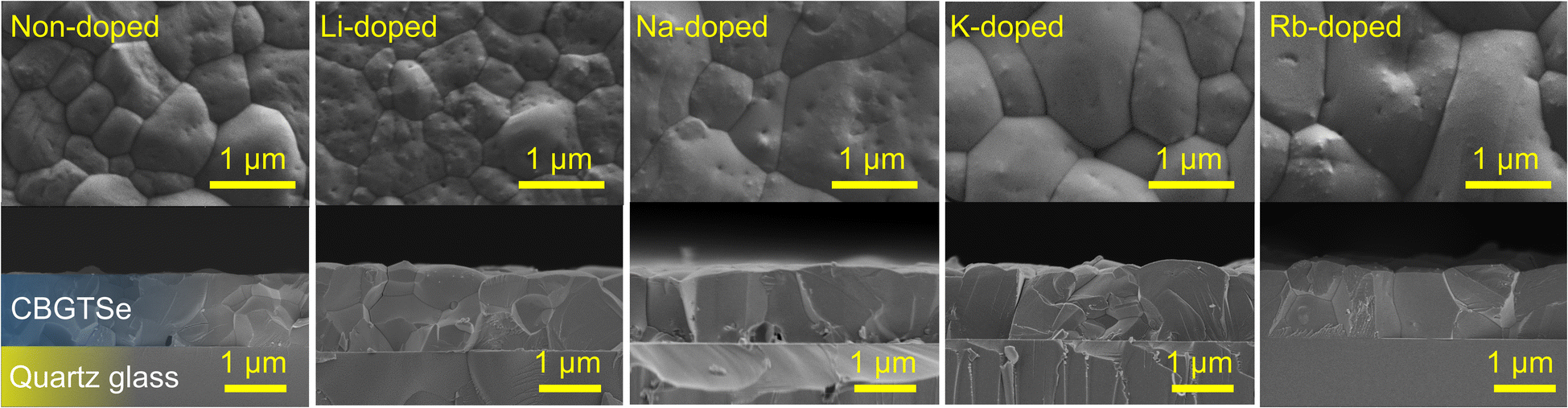 | ||
| Fig. 1 Surface/cross-section SEM images of non-doped and alkali-(i.e., Li, Na, K, and Rb) doped CBGTSe films deposited on quartz glass substrates. All scale bars represent 1 μm. Note that the alkali-doping was achieved by pre-depositing approximately 4-nm-thick layers of alkali fluoride (e.g., KF). Cross-section images were acquired after depositing ∼5 nm of Au to avoid surface charging. | ||
XRD patterns have also been acquired for all alkali-doped films (Fig. 2), and do not indicate any significant difference relative to non-doped films in terms of peak positions and phase purities (i.e., all samples are single phase according to XRD patterns). Pawley phase fitting, lattice constants (a and c), and lattice volumes (V) for the non-doped and alkali-doped CBGTSe films are summarized in Fig. S2.† Despite the largest incorporated amount (∼0.47 at%), Li-doping did not noticeably change the lattice constants (i.e., the changes observed are within the uncertainty). On the other hand, other alkali dopants (i.e., Na, K, and Rb) may lead to a slight increase in the lattice constants (although the differences are just marginally outside the margin of error), possibly indicating that the insertion of the alkali elements with larger size may expand the lattice cell volume of CBGTSe. Photoluminescence (PL) spectra of the non-doped and alkali-doped CBGTSe films have also been acquired (Fig. S3†). The PL peaks are somewhat unsymmetric over the ∼1.64–1.69 eV region, possibly reflecting limited local fluctuations in Sn/(Sn + Ge) composition within the films.48 Regardless of the alkali content, the PL positions (i.e., defined as the midpoint of the peak) were within the comparable range of 1.66–1.69 eV.
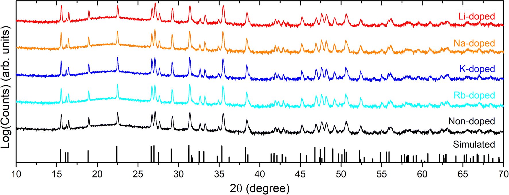 | ||
| Fig. 2 XRD patterns for CBGTSe films with different dopants, plotted on a log scale to accentuate any possible impurities. The simulated XRD stick pattern for CBGTSe (x = 0.7) was simulated using CrystalDiffract software with lattice parameters adapted from Wessler et al.48 XRD patterns of the doped CBGTSe films exhibit only the simulated peaks of the main phase, which excludes significant formation of secondary phases. | ||
3.2. Time-of-flight secondary ion mass spectrometry (TOF-SIMS)
The incorporation of alkali elements within the film does not necessarily imply uniform distribution within the absorber layer or within the structure (as assumed, for example, for the ICP-MS analysis; see Table 1). To identify the position of the alkali dopants in the CBGTSe films prepared with pre-deposition of 4 nm alkali fluoride layers, TOF-SIMS measurements were performed for the non-doped and alkali-doped samples. TOF-SIMS elemental depth profiles (Fig. S4†) reveal that the alkali dopants have relatively uniform distribution across the thickness of the CBGTSe films for all dopant types, rather than significantly being segregated at the top or bottom film interfaces.TOF-SIMS 2D images were also acquired by integrating the signal intensities of 3D tomography over the bulk region (approximately 0.2–0.6 μm depth) of the films to investigate how the alkali elements distribute across the film area. We note that the signal intensities in the TOF-SIMS 2D images are significantly influenced by film roughness as shown in total signal images (Fig. 3). Therefore, to reduce the influence of film roughness on the data, the isolated alkali signals are point-by-point normalized relative to the total signal (Fig. 3). For comparison, analogous images without such normalization are summarized in Fig. S5.† In Fig. 3, the noticeably darker spots in the total signal images may correspond to uncovered parts of the quartz glass substrate (i.e., pinholes). Both K-doped and Rb-doped samples show a few micron-wide regions near the uncovered area (i.e., pinholes) with a relatively higher concentration of alkali elements, possibly pointing to either a segregation of alkali elements to certain grain boundary regions or the presence of a small amount of alkali-rich secondary phase, which was not detected from XRD patterns (Fig. 2). In contrast, in the case of the area covered by the CBGTSe film, the alkali signals are detected strongly across the entire measured area for K- and Rb-doped films (Fig. 3), indicating that K and Rb dopants incorporate throughout the grain; some slightly higher intensity regions may indicate a small degree of elemental segregation of alkali dopants into the grain boundaries or slightly different alkali contents within different grains.
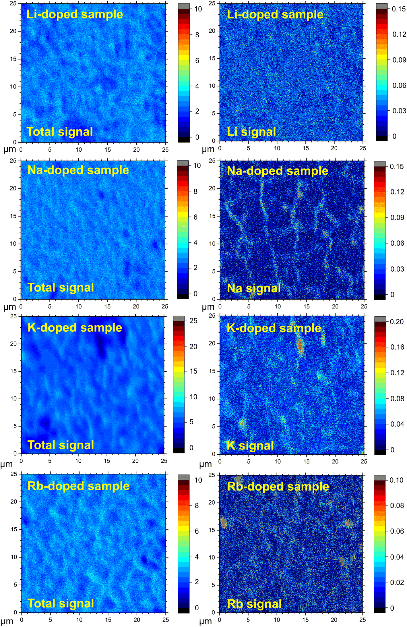 | ||
| Fig. 3 TOF-SIMS 2D images of alkali-doped CBGTSe films prepared with pre-deposition of 4 nm alkali fluoride layers showing (left) total signal counts and (right) alkali-element signals. Each image was obtained by integrating the signals over 0.2–0.6 μm film depth. Alkali-element signals are normalized point-by-point to the total signal counts to reduce the impact of film roughness on the alkali-element distribution images. Each image is 25 μm × 25 μm and the color scale shows the intensity of the signal per pixel (arb. units). | ||
Na signals in the Na-doped film show significantly non-uniform distribution over the film area with relatively higher signal intensities in the region that may correspond to the grain boundaries of the films (or some subset of grain boundaries). It is noteworthy that, despite the largest substitution amount for Li (∼0.47 at% according to ICP-MS), the Li-doped film shows the most uniform distribution of the dopants (i.e., no noticeable segregation of Li is detected), suggesting that the solubility of Li within the CBGTSe phase appears to be sufficient to allow for incorporation of this level of the dopant. Relatively more severe segregation of Na in the Na-doped film may reflect a relatively inferior degree of Na solubility compared to Li within the CBGTSe phase. We note that segregation of Na into grain boundaries has also been reported for other chalcogenides (e.g., CIGS,61,62 and CZTS63,64). Different degrees of alkali element solubility may relate to ionic size and coordination requirements for the Cu (relative to Li) and Ba (relative to K and Rb) sites within the CBGTSe structure.
3.3. Hall effect analysis
Hall effect measurements were conducted using a parallel dipole line-based Hall measurement setup. In addition to the samples pre-deposited with 4 nm alkali fluoride layers (predominantly discussed above), CBGTSe films with lower alkali content via pre-depositing thinner (i.e., 1 nm and 2 nm) alkali fluoride layers were also analyzed to check the systematic effect of alkali species and content on overall Hall effect parameters (i.e., carrier density and Hall mobility) (Fig. 4 and Table S1†). Examples of Hall coefficient extractions from the PDL setup for CBGTSe samples pre-deposited with different thicknesses of KF layers (0 nm, 1 nm, 2 nm, and 4 nm-thick) are shown in Fig. S6 and S7.† All CBGTSe films prepared in this study showed p-type conductivity. Non-doped CBGTSe films show limited carrier concentrations, with p < 1013 cm−3. Regardless of the type of alkali elements, the doped samples point to increasing carrier density values with increasing pre-deposition thickness of alkali fluoride, indicating that all types of alkali elements (i.e., Li, Na, K, and Rb) may be forming acceptor levels within CBGTSe, and in turn provide a pathway for increasing hole carrier density, p. The increase in p was most significant for K-doped samples—i.e., the CBGTSe films prepared with pre-deposition of 4 nm KF layers showed approximately three orders of magnitude increases in p values, reaching above 1015 cm−3.The doping efficiencies for each element were determined using the measured average hole carrier density (Table S1†) divided by the total density of the alkali element (Table 1) for the CBGTSe films, prepared by pre-depositing 4 nm alkali fluoride layers. The estimated (apparent) doping efficiencies are ∼10−5% for Li, ∼10−3% for Na, ∼8 × 10⁻³% for K, and ∼10−3% for Rb. Overall, Na, K, and Rb showed several orders of magnitude higher doping efficiencies than Li, while K showed the highest value among this group. Prospectively, enhanced doping efficiency for K may arise from the more similar atomic sizes of K (1.51 Å) and Ba (1.42 Å),43 in comparison with the other alkali elements (contributing to possibly a relatively higher density for K substituting on Ba sites). On the other hand, according to a theoretical study,65 the energy required for Li to substitute for Cu and form a LiCu anti-site defect has been reported to be noticeably lower compared to that required for other alkali metals such as Na and K for Cu2ZnSnS4, Cu2ZnSnSe4, and CuInS2. Besides, the cationic size for Li+ (0.59 Å) is comparable to Cu+ (0.60 Å), as opposed to Ba2+ (1.42 Å).43 Thus, for CBGTSe, Li may prefer forming charge-neutral LiCu anti-sites over LiBa acceptors (or/and potentially Lii interstitial donor defects due to its small cationic size), perhaps contributing to the significantly lower doping efficiency for the Li dopant in this study.
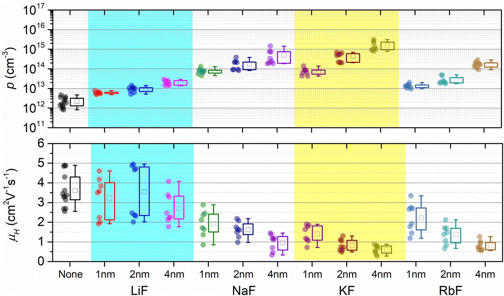 | ||
| Fig. 4 Statistical distribution of the hole carrier densities (p) and Hall mobilities (μH) extracted from Hall measurements on multiple (8–13) distinct non-doped and alkali-doped CBGTSe samples. The alkali concentration was controlled by varying the thickness of alkali fluoride layers (i.e., LiF, NaF, KF, and RbF) between 1 nm and 4 nm pre-deposited prior to CBGTSe films. The boxes are determined using (average) ± (standard deviation), the “□” symbols represent the average values, and the whiskers represent maximum and minimum data points. | ||
The doping efficiency (i.e., the ratio of the incremental hole carrier concentration to the added dopant concentration) even for K is still far below 1%. So far, there are only a few other literature reports targeting doping in related material systems (e.g., Ag2BaSnSe4 (ref. 21 and 23)). According to these studies, the Na dopant also exhibits relatively limited doping efficiency (≪1%) for Ag2BaSnSe4,21 which agrees with the observations from the current study. In contrast, In and Ga dopants are reported to have noticeably higher doping efficiencies of ∼0.7–2%.23 The limited doping efficiencies for alkali dopants for CBGTSe (as well as for Ag2BaSnSe4 and possibly other Cu2–II–IV–X4 compounds) might relate to the following factors: (1) the energetic positions for the associated shallow acceptor levels may be relatively far from the valence band maximum (VBM), which can lead to inefficient ionization, (2) alkali-dopants may also form charge-neutral (e.g., LiCu) and/or compensating donor (e.g., Lii) defects in addition to acceptor defects (e.g., LiBa), and/or (3) alkali elements may have only limited solubility within the crystal structure of CBGTSe, leading to grain boundary segregation of the alkali elements.
It is noteworthy that increasing alkali content also leads to an overall reduction in Hall mobility values (Fig. 4). A hole carrier density (p) vs. Hall mobility (μH) plot for the CBGTSe films from this study, as well as for vacuum-deposited CBGSe, CBTS, and ACBGTSe films reported from previous studies,24,27 are summarized in Fig. 5. p and μHvs. dopant concentration plots are also summarized in Fig. S8.†Fig. 5 suggests a universal trend showing a reduction in Hall mobility with increasing hole carrier density, encompassing all vacuum-deposited films. We note that the reduction in mobility with increasing doping density has also been observed for other semiconductor systems (e.g., GaAs,66 GaP,66 InP,66 (In,Ga)P,66 and InSb67). Charge carrier mobility can be limited by various mechanisms, including ionized impurity scattering, optical/acoustic phonon scattering, and grain boundary scattering.66–69 The first two mechanisms occur within the grain interior and are independent of grain sizes and grain boundaries. On the other hand, the third mechanism is not governed by the grain interior but by thermionic field emission of carriers over the barrier along grain boundaries, whose height can be affected by the doping level.69 However, the detailed mobility-limiting mechanisms for the I2–II–IV–X4 films have not been investigated yet. For a better understanding of the alkali-related acceptor-levels, carrier scattering mechanisms, and nature of grain boundaries for the alkali-doped and non-doped CBGTSe, CBGSe, CBTS, and ACBGTSe films, additional measurements (e.g., the temperature-dependent Hall effect and Kelvin probe force microscopy, which are beyond the scope of the current study) would be useful to reveal the following information: (1) the activation energies for these acceptor-levels, (2) the mobility-limiting mechanisms, and (3) the presence and height of potential barriers at grain boundaries.
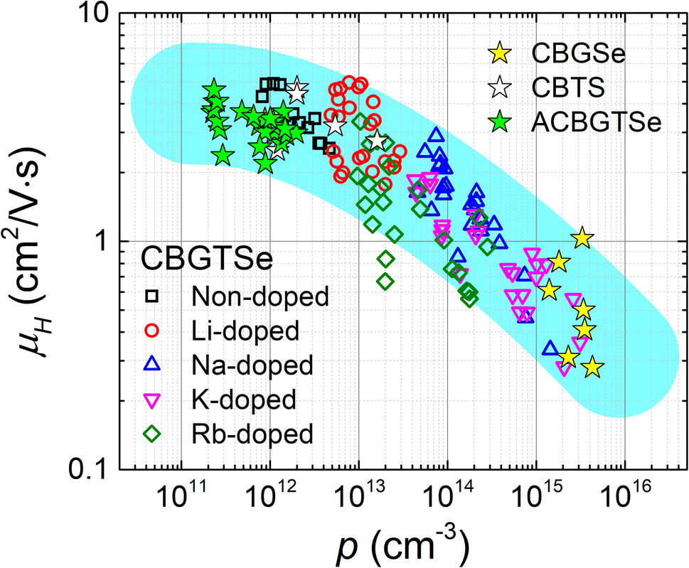 | ||
| Fig. 5 Hole carrier density (p) vs. Hall mobility (μH) plot summarizing all data points in Fig. 4. The data from previous studies on “non-doped” Cu2BaGeSe4 (CBGSe),24 Cu2BaSnS4 (CBTS),24 and Ag-alloyed CBGTSe (ACBGTSe)27 are also included in the plot and illustrated with star symbols (“☆”). The cyan-colored shading is a guide to the eye showing an apparent correlation between Hall mobilities and hole carrier densities over a wide range of carrier densities. | ||
3.4. Optical pump terahertz probe spectroscopy (OPTP)
Charge carrier recombination and transport properties for non-doped and alkali-doped CBGTSe films were examined using optical pump terahertz probe (OPTP) spectroscopy. For all samples, photoconductivity transient curves derived from OPTP show an initial fast decay of photoconductivity followed by a longer decay (Fig. 6). To derive decay time constants (τ1 and τ2) for the fast and slow decay components, two separate exponential decay functions (∝exp(−t/τ1,2)) were used for fitting the photoconductivity transient curve (Fig. S9†). The faster decay time constants (τ1) have values of 3–6 ps, while the slower time constants are approximately τ2 = 0.9–1.5 ns (Fig. S9† and Table 2). Fast and slow decay components were also observed for other Cu-based chalcogenides—i.e., CBTS,24 CBGSe,24 CBTSSe,13 and CZTS.70 In previous OPTP analysis with two different excitation wavelengths (400 nm and 800 nm) for a similar system (i.e., CBTSSe),13 the fast decay (with time constants of ∼10 ps) and the slower decay (∼ns) components have been attributed to surface and bulk recombination, respectively.13,70 Similarly, an additional excitation source with a wavelength of 400 nm < λ < 720 nm would facilitate clarifying the influence of surface recombination in the CBGTSe films, but such an excitation source is not currently available in our experimental setup. Considering the short penetration depths for the excitation source (∼30 nm penetration depth for 400 nm wavelength27) and similarities in materials and processing conditions between CBGTSe and previously studied lower band gap CBTSSe,13 the fast initial decay shown in Fig. 6 for the CBGTSe films may reasonably be attributed at least in part to surface recombination. In solar cell devices, the initial fast decay (possibly owing to surface recombination) may be a dominant recombination pathway, exacerbated by cliff-type CBO when a CdS buffer layer is used, limiting device performance. The few ns bulk minority carrier lifetimes for both non-doped and alkali-doped CBGTSe films are also, however, significantly shorter than lifetimes of state-of-the-art chalcopyrite or perovskite materials, which can reach several hundred nanoseconds to microseconds.71–73 Furthermore, all alkali-doped samples exhibit even shorter decay times (τ1 = 2.9–5.0 ps and τ2 = 0.9–1.3 ns) than non-doped samples (τ1 = 5.8 ps and τ2 = 1.5 ns). Shorter decay times, τ1 and τ2, point to higher surface recombination velocity (∝1/τ1) and bulk recombination rates (∝1/τ2), indicating that alkali-doping likely creates additional defects that may serve as recombination centers.
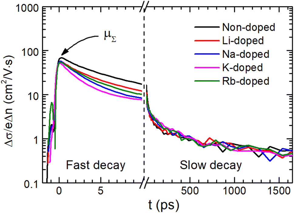 | ||
| Fig. 6 THz photoconductivity transient curves obtained from non-doped and alkali-doped (pre-deposited with 4 nm of alkali fluoride layers) CBGTSe films, showing fast-/slow-decaying components, and terahertz sum mobilities (μΣ). | ||
| Sample | τ 1 (ps) | τ 2 (ns) | μ Σ (cm2 V−1 s−1) | μ H (cm2 V−1 s−1) |
|---|---|---|---|---|
| Non-doped | 5.8 ± 0.1 | 1.5 ± 0.3 | 68.6 | 3.62 |
| Li-doped | 5.0 ± 0.1 | 1.2 ± 0.1 | 55.9 | 2.70 |
| Na-doped | 3.5 ± 0.1 | 1.1 ± 0.2 | 57.4 | 0.98 |
| K-doped | 2.9 ± 0.1 | 0.9 ± 0.1 | 52.0 | 0.61 |
| Rb-doped | 4.6 ± 0.1 | 1.3 ± 0.2 | 54.6 | 0.81 |
Additionally, the terahertz sum mobility values, μΣ, of the CBGTSe films were also estimated by OPTP (Fig. S9† and Table 2). As for the time constants (τ1 and τ2), sum mobility values for alkali-doped samples (52.0–57.4 cm2 V−1 s−1) show relatively lower values than that for the non-doped sample (68.6 cm2 V−1 s−1). In particular, the μΣ value for the K-doped sample is the lowest (52.0 cm2 V−1 s−1) among all alkali-doped samples. The terahertz sum mobility estimated from OPTP should primarily reflect the carrier transport properties within grain interiors.74 Thus, the reduced terahertz sum mobilities for the alkali-doped CBGTSe films compared to the non-doped sample indicate that alkali dopants (i.e., Li, Na, K, and Rb) may form scattering centers, which could correspond to ionized defects associated with the alkali dopants. Besides, the reductions in Hall mobility values observed for alkali-doped films are relatively more significant compared to analogous values from terahertz sum mobility. Such different effects may originate from (1) transport of hole carriers via an acceptor band created by dopants70 or/and (2) grain boundary scattering mechanisms enhanced by doping.69 It is also noteworthy that a terahertz sum mobility value of 68.6 cm2 V−1 s−1, even for the non-doped CBGTSe sample, is noticeably lower than the 140 cm2 V−1 s−1 value for CBTSSe13 and 135 cm2 V−1 s−1 for CZTS,70 implying that scattering sites may impact charge carrier transport for CBGTSe.
4. Conclusion
In this study, alkali elements (i.e., Li, Na, K, and Rb) were investigated as prospective p-type dopants to enhance the low hole carrier concentration (∼1012 cm−3) of intrinsic CBGTSe films. The maximum quantities of the alkali dopants incorporated into the CBGTSe films were estimated to be ∼0.47 at% for Li, ∼0.11 at% for Na, ∼0.05 at% for K, and ∼0.03 at% for Rb according to ICP-MS. Due to the incorporation of these dopants into the lattice, the alkali-doped CBGTSe films showed at most small changes (<0.1%) in lattice constants compared to the non-doped films. Additionally, SEM images reveal that Na-, K-, and Rb-doped CBGTSe films have significantly increased average grain sizes compared to the non-doped film, while the changes in the grain size are negligible for Li. TOF-SIMS elemental depth profiles show that the distributions of alkali dopants across the thickness of the CBGTSe films are relatively uniform. Besides, TOF-SIMS 3D tomography suggests that Li, K, and Rb dopants mostly incorporate uniformly rather than segregating into the grain boundaries. On the other hand, Na-doped samples show a noticeably inhomogeneous distribution of Na across the film surface, possibly indicating that a larger portion of this dopant segregates into the grain boundaries. The Hall effect reveals that incorporation of the alkali dopants induces hole carrier density increases by up to 1–3 orders of magnitude with the alkali-doping. The increase is most notable for the K dopant, which achieves a hole carrier density of up to p = ∼1.6 × 1015 cm−3, while the increase is the smallest for Li (p = ∼2.0 × 1013 cm−3). However, the doping efficiency is still largely limited even for the K dopant (∼8 × 10⁻³%). The photoconductivity transient curves from OPTP analyses show that the alkali-doped films have slightly shorter minority carrier lifetimes compared to the non-doped films. Furthermore, both Hall mobilities and terahertz sum mobilities show a noticeable reduction for the alkali-doped samples, indicating that the alkali-dopants limit carrier transport properties for the CBGTSe films. As we have shown an increase in the carrier concentration by up to 3 orders of magnitude, alkali-doping can be considered a useful approach for semiconductor tuning (e.g., for PV, thermoelectric and photoelectrochemical devices) for CBGTSe and analogous I2–II–IV–X4 chalcogenide compounds. Future studies will target increased minority carrier lifetime and charge carrier mobility in the CBGTSe films through appropriate film processing modifications and defect passivation to improve the film properties.Conflicts of interest
There are no conflicts to declare.Acknowledgements
This material is based upon work supported by the U. S. Department of Energy, Office of Science, Basic Energy Sciences (BES), under contract DE-SC0020061. This work was performed in part at the Duke University Shared Materials Instrumentation Facility (SMIF), a member of the North Carolina Research Triangle Nanotechnology Network (RTNN), which is supported by the National Science Foundation (award number ECCS-2025064) as part of the National Nanotechnology Coordinated Infrastructure (NNCI). All opinions expressed in this paper are the authors' and do not necessarily reflect the policies and views of the U.S. DOE or NSF. This work was authored in part by the National Renewable Energy Laboratory, operated by Alliance for Sustainable Energy, LLC, for the U.S. Department of Energy (DOE) under Contract No. DE-AC36-08GO28308. The views expressed in the article do not necessarily represent the views of the DOE or the U.S. Government. The U.S. Government retains and the publisher, by accepting the article for publication, acknowledges that the U.S. Government retains a nonexclusive, paid-up, irrevocable, worldwide license to publish or reproduce the published form of this work, or allow others to do so, for U.S. Government purposes.References
- T. Zhu, W. P. Huhn, G. C. Wessler, D. Shin, B. Saparov, D. B. Mitzi and V. Blum, Chem. Mater., 2017, 29, 7868–7879 CrossRef CAS.
- J.-P. Sun, G. C. McKeown Wessler, T. Wang, T. Zhu, V. Blum and D. B. Mitzi, Chem. Mater., 2020, 32, 1636 CrossRef CAS.
- D. B. Mitzi and Y. Kim, Faraday Discuss., 2022, 239, 9 RSC.
- S. Chen, A. Walsh, X. G. Gong and S. H. Wei, Adv. Mater., 2013, 25, 1522–1539 CrossRef CAS PubMed.
- S. Chen, L.-W. Wang, A. Walsh, X. Gong and S.-H. Wei, Appl. Phys. Lett., 2012, 101, 223901 CrossRef.
- K. Biswas, S. Lany and A. Zunger, Appl. Phys. Lett., 2010, 96, 201902 CrossRef.
- S. Bourdais, C. Choné, B. Delatouche, A. Jacob, G. Larramona, C. Moisan, A. Lafond, F. Donatini, G. Rey and S. Siebentritt, Adv. Energy Mater., 2016, 6, 1502276 CrossRef.
- D. B. Mitzi, O. Gunawan, T. K. Todorov and D. A. R. Barkhouse, Philos. Trans. R. Soc., A, 2013, 371, 20110432 CrossRef PubMed.
- T. Gokmen, O. Gunawan, T. K. Todorov and D. B. Mitzi, Appl. Phys. Lett., 2013, 103, 103506 CrossRef.
- T. Gokmen, O. Gunawan and D. B. Mitzi, Appl. Phys. Lett., 2014, 105, 033903 CrossRef.
- D. Shin, B. Saparov, T. Zhu, W. P. Huhn, V. Blum and D. B. Mitzi, Chem. Mater., 2016, 28, 4771–4780 CrossRef CAS.
- B. Teymur, Y. Zhou, E. Ngaboyamahina, J. T. Glass and D. B. Mitzi, Chem. Mater., 2018, 30, 6116–6123 CrossRef CAS.
- B. Teymur, S. Levcenco, H. Hempel, E. Bergmann, J. A. Márquez, L. Choubrac, I. G. Hill, T. Unold and D. B. Mitzi, Nano Energy, 2020, 80, 105556 CrossRef.
- Z. Chen, K. Sun, Z. Su, F. Liu, D. Tang, H. Xiao, L. Shi, L. Jiang, X. Hao and Y. Lai, ACS Appl. Energy Mater., 2018, 1, 3420–3427 CrossRef CAS.
- D. Shin, T. Zhu, X. Huang, O. Gunawan, V. Blum and D. B. Mitzi, Adv. Mater., 2017, 29, 1606945 CrossRef PubMed.
- J. Ge, P. Koirala, C. R. Grice, P. J. Roland, Y. Yu, X. Tan, R. J. Ellingson, R. W. Collins and Y. Yan, Adv. Energy Mater., 2017, 7, 1601803 CrossRef.
- J. Ge, Y. Yu and Y. Yan, ACS Energy Lett., 2016, 1, 583–588 CrossRef CAS.
- B. Teymur, Y. Kim, J. Huang, K. Sun, X. Hao and D. B. Mitzi, Adv. Energy Mater., 2022, 12, 2201602 CrossRef CAS.
- Y. Zhou, D. Shin, E. Ngaboyamahina, Q. Han, C. B. Parker, D. B. Mitzi and J. T. Glass, ACS Energy Lett., 2017, 3, 177–183 CrossRef.
- D. Shin, E. Ngaboyamahina, Y. Zhou, J. T. Glass and D. B. Mitzi, J. Phys. Chem. Lett., 2016, 7, 4554–4561 CrossRef CAS PubMed.
- J. J. Kuo, U. Aydemir, J.-H. Pöhls, F. Zhou, G. Yu, A. Faghaninia, F. Ricci, M. A. White, G.-M. Rignanese and G. Hautier, J. Mater. Chem. A, 2019, 7, 2589–2596 RSC.
- A. Hong and L. Ma, Appl. Phys. Lett., 2021, 118, 143903 CrossRef CAS.
- Y. Li, Z. Li, C. Zhang, D. Yang, T. Liu, Y. Yan, W. Liu, G. Tan, X. Su and C. Uher, Mater. Today Phys., 2019, 9, 100098 CrossRef.
- Y. Kim, H. Hempel, S. Levcenko, J. Euvrard, E. Bergmann, G. Oki, T. Unold, I. G. Hill and D. B. Mitzi, J. Mater. Chem. A, 2021, 9, 23619–23630 RSC.
- T. Minemoto, T. Matsui, H. Takakura, Y. Hamakawa, T. Negami, Y. Hashimoto, T. Uenoyama and M. Kitagawa, Sol. Energy Mater. Sol. Cells, 2001, 67, 83–88 CrossRef CAS.
- Y. Kim and D. B. Mitzi, ACS Appl. Energy Mater., 2021, 4, 11528–11536 CrossRef CAS.
- Y. Kim, H. Hempel, T. Unold and D. B. Mitzi, Sol. RRL, 2023, 7, 2201058 CrossRef CAS.
- A. Nagaoka, Y. Nose, H. Miyake, M. A. Scarpulla and K. Yoshino, Renewable Energy, 2015, 79, 127–130 CrossRef CAS.
- T. Meyer, F. Engelhardt, J. Parisi and U. Rau, J. Appl. Phys., 2002, 91, 5093–5099 CrossRef CAS.
- T. Gershon, Y. S. Lee, P. Antunez, R. Mankad, S. Singh, D. Bishop, O. Gunawan, M. Hopstaken and R. Haight, Adv. Energy Mater., 2016, 6, 1502468 CrossRef.
- O. Gunawan, S. R. Pae, D. M. Bishop, Y. Virgus, J. H. Noh, N. J. Jeon, Y. S. Lee, X. Shao, T. Todorov and D. B. Mitzi, Nature, 2019, 575, 151–155 CrossRef CAS PubMed.
- A. Kanevce, M. O. Reese, T. Barnes, S. Jensen and W. Metzger, J. Appl. Phys., 2017, 121, 214506 CrossRef.
- J. Perrenoud, L. Kranz, C. Gretener, F. Pianezzi, S. Nishiwaki, S. Buecheler and A. Tiwari, J. Appl. Phys., 2013, 114, 174505 CrossRef.
- J. M. Burst, S. B. Farrell, D. S. Albin, E. Colegrove, M. O. Reese, J. N. Duenow, D. Kuciauskas and W. K. Metzger, APL Mater., 2016, 4, 116102 CrossRef.
- S. Kim, D. Kim, J. Hong, A. Elmughrabi, A. Melis, J.-Y. Yeom, C. Park and S. Cho, Materials, 2022, 15, 1408 CrossRef CAS PubMed.
- A. Onno, C. Reich, S. Li, A. Danielson, W. Weigand, A. Bothwell, S. Grover, J. Bailey, G. Xiong and D. Kuciauskas, Nat. Energy, 2022, 7, 400–408 CrossRef CAS.
- E. Colegrove, J. Yang, S. Harvey, M. Young, J. Burst, J. Duenow, D. Albin, S. Wei and W. Metzger, J. Phys. D: Appl. Phys., 2018, 51, 075102 CrossRef.
- Y. Sun, S. Lin, W. Li, S. Cheng, Y. Zhang, Y. Liu and W. Liu, Engineering, 2017, 3, 452–459 CrossRef CAS.
- D. S. Dhawale, A. Ali and A. C. Lokhande, Sustainable Energy Fuels, 2019, 3, 1365–1383 RSC.
- T. Gershon, B. Shin, N. Bojarczuk, M. Hopstaken, D. B. Mitzi and S. Guha, Adv. Energy Mater., 2015, 5, 1400849 CrossRef.
- N. Nicoara, R. Manaligod, P. Jackson, D. Hariskos, W. Witte, G. Sozzi, R. Menozzi and S. Sadewasser, Nat. Commun., 2019, 10, 3980 CrossRef PubMed.
- T.-Y. Lin, I. Khatri, J. Matsuura, K. Shudo, W.-C. Huang, M. Sugiyama, C.-H. Lai and T. Nakada, Nano Energy, 2020, 68, 104299 CrossRef CAS.
- R. D. Shannon, Acta Crystallogr., Sect. A: Cryst. Phys., Diffr., Theor. Gen. Crystallogr., 1976, 32, 751–767 CrossRef.
- O. Gunawan, Y. Virgus and K. F. Tai, Appl. Phys. Lett., 2015, 106, 062407 CrossRef.
- S. P. Harvey, J. Messinger, K. Zhu, J. M. Luther and J. J. Berry, Adv. Energy Mater., 2020, 10, 1903674 CrossRef CAS.
- S. P. Harvey, F. Zhang, A. Palmstrom, J. M. Luther, K. Zhu and J. J. Berry, ACS Appl. Mater. Interfaces, 2019, 11, 30911–30918 CrossRef CAS PubMed.
- S. P. Harvey, Z. Li, J. A. Christians, K. Zhu, J. M. Luther and J. J. Berry, ACS Appl. Mater. Interfaces, 2018, 10, 28541–28552 CrossRef CAS PubMed.
- G. C. Wessler, T. Zhu, J.-P. Sun, A. Harrell, W. P. Huhn, V. Blum and D. B. Mitzi, Chem. Mater., 2018, 30, 6566–6574 CrossRef CAS.
- A. Pugh and R. Barrow, Trans. Faraday Soc., 1958, 54, 671–678 RSC.
- M. Eisenstadt, G. Rothberg and P. Kusch, J. Chem. Phys., 1958, 29, 797–804 CrossRef CAS.
- J. Sangster and A. Pelton, J. Phase Equilib., 1997, 18, 185 CrossRef CAS.
- J. Sangster and A. Pelton, J. Phase Equilib., 1997, 18, 177 CrossRef CAS.
- J. Sangster and A. Pelton, J. Phase Equilib., 1997, 18, 190–193 CrossRef CAS.
- J. Sangster and A. Pelton, J. Phase Equilib., 1997, 18, 181 CrossRef CAS.
- H. Ipser, M. Gambino and W. Schuster, Monatsh. Chem., 1982, 113, 389–398 CrossRef CAS.
- S. Kim, K. M. Kim, H. Tampo, H. Shibata, K. Matsubara and S. Niki, Sol. Energy Mater. Sol. Cells, 2016, 144, 488–492 CrossRef CAS.
- D. B. Khadka and J. Kim, J. Phys. Chem. C, 2015, 119, 1706–1713 CrossRef CAS.
- R. M. German, P. Suri and S. J. Park, J. Mater. Sci., 2009, 44, 1–39 CrossRef CAS.
- S. Engberg, S. Canulescu and J. Schou, RSC Adv., 2018, 8, 7152–7158 RSC.
- S. Y. Kim, D. H. Son, S. H. Kim, Y. I. Kim, S. Kim, K. Ahn, K. J. Yang, J. K. Kang and D. H. Kim, Adv. Energy Mater., 2020, 10, 1903173 CrossRef CAS.
- M. S. Bodegard, L. Stolt and J. Hedstrom, Proc. 12th European Photovoltaic Solar Energy Conference, 1994, pp. 1743–1746 Search PubMed.
- O. Cojocaru-Mirédin, P.-P. Choi, D. Abou-Ras, S. S. Schmidt, R. Caballero and D. Raabe, IEEE J. Photovolt., 2011, 1, 207–212 Search PubMed.
- S. Tajima, R. Asahi, D. Isheim, D. N. Seidman, T. Itoh and K.-i. Ohishi, Jpn. J. Appl. Phys., 2015, 54, 112302 CrossRef.
- J. Kim, G. Y. Kim, T. T. T. Nguyen, S. Yoon, Y.-K. Kim, S.-Y. Lee, M. Kim, D.-H. Cho, Y.-D. Chung and J.-H. Lee, Phys. Chem. Chem. Phys., 2020, 22, 7597–7605 RSC.
- T. Maeda, A. Kawabata and T. Wada, Phys. Status Solidi C, 2015, 12, 631–637 CrossRef CAS.
- M. Sotoodeh, A. Khalid and A. Rezazadeh, J. Appl. Phys., 2000, 87, 2890–2900 CrossRef CAS.
- K. W. Boer and U. W. Pohl, Semiconductor Physics, Springer Berlin Heidelberg, 2018 Search PubMed.
- A. Di Carlo, F. Piacenza, A. Bolognesi, B. Stadlober and H. Maresch, Appl. Phys. Lett., 2005, 86, 263501 CrossRef.
- J. Y. Seto, J. Appl. Phys., 1975, 46, 5247–5254 CrossRef CAS.
- H. Hempel, C. J. Hages, R. Eichberger, I. Repins and T. Unold, Sci. Rep., 2018, 8, 1–9 CAS.
- E. Gutierrez-Partida, H. Hempel, S. Caicedo-Davila, M. Raoufi, F. Pena-Camargo, M. Grischek, R. Gunder, J. Diekmann, P. Caprioglio and K. O. Brinkmann, ACS Energy Lett., 2021, 6, 1045–1054 CrossRef CAS.
- W. K. Metzger, I. L. Repins and M. A. Contreras, Appl. Phys. Lett., 2008, 93, 022110 CrossRef.
- M. Ochoa, S. C. Yang, S. Nishiwaki, A. N. Tiwari and R. Carron, Adv. Energy Mater., 2022, 12, 2102800 CrossRef CAS.
- H. Hempel, T. J. Savenjie, M. Stolterfoht, J. Neu, M. Failla, V. C. Paingad, P. Kužel, E. J. Heilweil, J. A. Spies and M. Schleuning, Adv. Energy Mater., 2022, 12, 2102776 CrossRef CAS.
Footnote |
| † Electronic supplementary information (ESI) available. See DOI: https://doi.org/10.1039/d3ta01494k |
| This journal is © The Royal Society of Chemistry 2023 |